EP1008997B1 - Inductance à haute fréquence à grand coefficient de qualité - Google Patents
Inductance à haute fréquence à grand coefficient de qualité Download PDFInfo
- Publication number
- EP1008997B1 EP1008997B1 EP99124485A EP99124485A EP1008997B1 EP 1008997 B1 EP1008997 B1 EP 1008997B1 EP 99124485 A EP99124485 A EP 99124485A EP 99124485 A EP99124485 A EP 99124485A EP 1008997 B1 EP1008997 B1 EP 1008997B1
- Authority
- EP
- European Patent Office
- Prior art keywords
- inductor
- spiral
- inductor elements
- pairs
- layer
- Prior art date
- Legal status (The legal status is an assumption and is not a legal conclusion. Google has not performed a legal analysis and makes no representation as to the accuracy of the status listed.)
- Expired - Lifetime
Links
Images


Classifications
-
- H—ELECTRICITY
- H01—ELECTRIC ELEMENTS
- H01F—MAGNETS; INDUCTANCES; TRANSFORMERS; SELECTION OF MATERIALS FOR THEIR MAGNETIC PROPERTIES
- H01F17/00—Fixed inductances of the signal type
- H01F17/0006—Printed inductances
-
- H—ELECTRICITY
- H01—ELECTRIC ELEMENTS
- H01F—MAGNETS; INDUCTANCES; TRANSFORMERS; SELECTION OF MATERIALS FOR THEIR MAGNETIC PROPERTIES
- H01F17/00—Fixed inductances of the signal type
- H01F17/0006—Printed inductances
- H01F17/0013—Printed inductances with stacked layers
-
- H—ELECTRICITY
- H01—ELECTRIC ELEMENTS
- H01F—MAGNETS; INDUCTANCES; TRANSFORMERS; SELECTION OF MATERIALS FOR THEIR MAGNETIC PROPERTIES
- H01F27/00—Details of transformers or inductances, in general
- H01F27/34—Special means for preventing or reducing unwanted electric or magnetic effects, e.g. no-load losses, reactive currents, harmonics, oscillations, leakage fields
-
- Y—GENERAL TAGGING OF NEW TECHNOLOGICAL DEVELOPMENTS; GENERAL TAGGING OF CROSS-SECTIONAL TECHNOLOGIES SPANNING OVER SEVERAL SECTIONS OF THE IPC; TECHNICAL SUBJECTS COVERED BY FORMER USPC CROSS-REFERENCE ART COLLECTIONS [XRACs] AND DIGESTS
- Y10—TECHNICAL SUBJECTS COVERED BY FORMER USPC
- Y10T—TECHNICAL SUBJECTS COVERED BY FORMER US CLASSIFICATION
- Y10T29/00—Metal working
- Y10T29/49—Method of mechanical manufacture
- Y10T29/49002—Electrical device making
- Y10T29/4902—Electromagnet, transformer or inductor
Definitions
- the present invention relates to an inductor having a high Q value for use in high frequency in a semiconductor integrated circuit (IC).
- IC semiconductor integrated circuit
- the reference numeral 1 denotes an inductor section
- 2 denotes a drawing interconnect formed in the first layer
- 3 denotes a drawing interconnect formed in the second layer
- 5 denotes a connection between the first and second layers
- 7 denotes an interlayer film
- 8 denotes a smoothing film.
- the inductor section is constructed of a single layer and the second layer is used for the drawing interconnect for connection with other components.
- EP-A-0 484 558 describes a high frequency inductor device comprising strip-like coil conductors formed on an insulating substrate.
- the inductor device includes a plurality of said strip-like coil conductors being arranged in plural layers and connected in parallel.
- the strip-like coil conductors are arranged such that an electric currents flowing through the conductors of the different layers has the same direction in corresponding conductor portions.
- US-A-4 641 118 describes an electromagnet utilizing a coil consisting of a plurality of insulating substrates. On each substrate, a spiral conductor is formed. The spiral direction of conductors is reversed on each of successive substrates. The spiral centers and outer ends of successive conductors are connected in an alternating fashion, such that a serial connection of the conductors is obtained.
- Figure 1 shows the first embodiment of the high-Q inductor for high frequency useful for the understanding of the present invention.
- the reference numeral 11 denotes a meander-type first-layer inductor section (the "inductor section” as used herein corresponds to an "inductor element” to be recited in the claims)
- 12 and 13 denote first-layer drawing interconnects
- 14 denotes a second-layer inductor section
- 15 and 16 denote connections between the first and second layers
- 17 denotes an interlayer film
- 18 denotes a smoothing film.
- connection 15 and 16 is composed of nine contact portions each having a size of about 1 ⁇ m square, for example.
- the inductor section which is conventionally constructed using only one layer, is of a two-layer structure where two inductor sections are formed in the first and second layers and connected in parallel with each other.
- the above construction makes it possible to obtain a high Q-value inductor for high frequency which overcomes the conventional problem of having a large serial resistance component in low frequency and high frequency and thus a lowered Q value, by increasing the cross section and suppressing lowering of the Q value which otherwise occurs due to a skin effect in high frequency.
- first and second layers may be connected in parallel over the entire inductor sections. This construction is also included in the present invention.
- Figure 2 shows the second embodiment of the high-Q inductor for high frequency useful for the understanding of the present invention.
- the reference numeral 21 denotes a spiral-shaped first-layer inductor section
- 22 denotes a first-layer drawing interconnect
- 23 denotes a spiral-shaped second-layer inductor section
- 24 denotes a drawing interconnect from the second-layer inductor section 23 formed in the third layer
- 25 and 26 denote connections between the first and second layers
- 27 and 28 denote interlayer films
- 29 denotes a smoothing film
- 210 denotes a connection between the second and third layers.
- the first-layer inductor section 22 and the second-layer inductor section 23 are spiraled in the same direction.
- the inductor section which is conventionally constructed using only one layer, is of a two-layer structure where the inductor sections22 and 23 are respectively formed in the first and second layers and connected in parallel with each other.
- This construction makes it possible to obtain a high Q-value inductor for high frequency which overcomes the conventional problem of having a large serial resistance component in low frequency and high frequency and thus a lowered Q value, by increasing the cross section and suppressing lowering of the Q value which otherwise occurs due to a skin effect in high frequency.
- first and second layers may be connected in parallel over the entire inductor sections. This construction is also included in the present invention.
- the three-layer inductor was exemplified. It is also possible to construct a similar structure composed of four or more layers with a drawing interconnect being formed in the bottom layer.
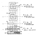
- Figure 3 shows the third embodiment of the high-Q inductor for high frequency according to the present invention.
- the reference numeral 31 denotes a spiral-shaped first-layer inductor section
- 32 denotes a first-layer drawing interconnect
- 33 denotes a spiral-shaped second-layer inductor section
- 34 denotes a second-layer drawing interconnect
- 35 denotes connections between the first and second layers
- 37 denotes an interlayer film
- 38 denotes a smoothing film.
- the first and second inductor sections 31 and 33 are connected in parallel with each other.
- Embodiment 3 is characterized in that the second-layer drawing interconnect 34 is formed using the layer in which the second-layer inductor section 33 is formed.
- the second-layer inductor section 33 is cut off at the positions where the drawing interconnect 34 crosses. The cut-off ends of the inductor section 33 are connected with the first-layer inductor section 31 via the connections 35.
- the second-layer inductor section 33 can serve as one substantially spiral-shaped inductor section.
- the inductor section which is conventionally constructed using only one layer, is of a two-layer structure where inductor sections are formed in the first and second layers and connected in parallel with each other. Furthermore, the inductor sections are formed in the layers in which the drawing interconnects are formed. As a result, it is possible, even in a process where a smaller number of wiring layers are used, to obtain a high Q-value inductor for high frequency which overcomes the conventional problem of having a large serial resistance component in low frequency and high frequency and thus a lowered Q value, by increasing the cross section and suppressing lowering of the Q value which otherwise occurs due to a skin effect in high frequency.
- Embodiment 3 is characterized in that one of the drawing interconnects is formed using the wiring layer for the inductor section, which is different from Embodiment 2 where the layer for forming the drawing interconnect is separately provided.
- first and second layers may be connected in parallel over the entire inductor sections. This construction is also included in the present invention.
- the two-layer inductor was exemplified. It is also possible to construct a similar structure composed of three or more layers with a drawing interconnect being formed in any of the layers. In this case, portions of an inductor section at which the drawing interconnect crosses can be connected with an adjacent upper or lower inductor section.
- Figures 7 and 8 are graphs showing comparison of performances of the two-layer inductor according to the present invention and a conventional one-layer inductor.
- Figure 7 is a graph obtained by plotting a variation of the resistance (R) with respect to the length (L). It is observed from this figure that R is smaller in the two-layer inductor according to the present invention.
- Figure 8 is a graph obtained by plotting a variation of the Q value (Q) with respect to the length (L). It is observed from this figure that Q is greater in the two-layer inductor according to the present invention.
- Figure 4 shows the fourth embodiment of the high-Q inductor for high frequency according to the present invention.
- the reference numeral 41 denotes a spiral-shaped first-layer inductor section
- 42 denotes a first-layer drawing interconnect
- 43 denotes a connection between the first and second layers
- 44 denotes a spiral-shaped second-layer inductor section
- 45 denotes a connection between the second and third layers
- 46 denotes a spiral-shaped third-layer inductor section
- 47 denotes a connection between the third and fourth layers
- 48 denotes a spiral-shaped fourth-layer inductor section
- 49 denotes a fourth-layer drawing interconnect
- 410, 411, and 412 denote interlayer films
- 413 denotes a smoothing film.
- the adjacent inductor sections are connected with each other. Specifically, the centers or the outer ends of the adjacent inductor sections are connected with each other. These inductor sections are therefore connected in series with each other.
- the second-layer and fourth-layer inductor sections have a shape inverted upside down from that of the first-layer and third-layer inductor sections.
- the directions of the magnetic fields generated by the respective inductor sections are the same, resulting in effective coupling.
- the four-layer structure was described in this embodiment. However, as shown in Figure 5, the number of layers may be increased to five or six, for example, in a similar structure. The structure is simpler when the number of layers is even, because the drawing interconnect can be formed to be connected with the outer end of the bottom inductor section.
- drawing interconnect can be arranged in a manner described in Figure 2 or 3.
- a pair of adjacent inductor sectors may have the same spiral direction, and adjacent pairs of adjacent inductor sectors may have different spiral directions.
- one inductor sector of one pair is connected with one of another pair as shown in Figure 6 so that all the inductor sectors are serially connected.
- the inductor section which is conventionally constructed of a single wiring layer, is of a multi-layer structure.
- a high Q-value inductor which has a reduced serial resistance component and is free from an influence of a skin effect can be fabricated in an IC.
Landscapes
- Engineering & Computer Science (AREA)
- Power Engineering (AREA)
- Microelectronics & Electronic Packaging (AREA)
- Coils Or Transformers For Communication (AREA)
Claims (4)
- Bobine d'inductance à haute fréquence à facteur de qualité élevé, comprenant une pluralité d'éléments d'inductance (31, 33) formés dans une pluralité de couches de câblage de circuit intégré respectivement, les directions des champs magnétiques générés par les éléments d'inductance respectifs (31, 33) étant pratiquement les mêmes,
où lesdits éléments d'inductance (31, 33) sont en forme de spirale et reliés en parallèle les uns aux autres, et
une électrode conductrice (34) formée dans une couche de câblage de circuit intégré est reliée au centre de spirale de l'un desdits éléments d'inductance en forme de spirale (31, 33),
caractérisée en ce que
ladite électrode conductrice (34) est formée dans une couche de câblage de circuit intégré dans laquelle l'un desdits éléments d'inductance en forme de spirale (33) est formé, et
l'élément d'inductance en forme de spirale (33) formé dans ladite couche de câblage de circuit intégré, dans laquelle ladite électrode conductrice (34) est formée, est découpé à des positions où l'électrode conductrice (34) traverse, et les extrémités découpées de l'élément d'inductance (33) sont reliées à des parties correspondantes respectives de l'élément d'inductance en forme de spirale (31) formé dans une autre des couches de câblage de circuit intégré. - Bobine d'inductance à haute fréquence à facteur de qualité élevé selon la revendication 1, dans laquelle une liaison (35) entre la pluralité d'éléments d'inductance en.forme de spirale (31, 33) est formée dans un film inter-couches (37) disposé entre les couches de câblage de circuit intégré dans lesquelles sont formés les éléments d'inductance en forme de spirale (31, 33).
- Bobine d'inductance à haute fréquence à facteur de qualité élevé, comprenant une pluralité d'éléments d'inductance (41, 44, 46, 48) formés dans une pluralité de couches de câblage de circuit intégré respectivement,
où la pluralité d'éléments d'inductance (41, 44, 46, 48) sont formés en forme de spirale respectivement, ladite chaque forme de spirale est formée de plusieurs groupes de deux paires de lignes droites qui s'opposent mutuellement,
les éléments d'inductance adjacents de la pluralité d'éléments d'inductance (41, 44, 46, 48) sont reliés les uns aux autres d'une manière telle que les éléments d'inductance adjacents sont reliés en série en reliant les centres de spirales (43, 47) de ceux-ci les uns aux autres et les extrémités extérieures (45) de ceux-ci les unes avec les autres, et
lesdits éléments d'inductance (41, 44, 46, 48) sont agencés de sorte qu'une zone sur laquelle se chevauchent (a) un premier groupe comprenant plusieurs premières paires desdites deux paires de lignes droites dont est formé ledit élément d'inductance agencé dans l'une desdites couches de câblage de circuit intégré et (b) un second groupe comprenant plusieurs premières paires desdites deux paires de lignes droites dont est formé ledit élément d'inductance agencé dans une autre desdites couches de câblage de circuit intégré, peut être plus petite qu'une zone avec laquelle se chevauchent (c) un troisième groupe comprenant plusieurs autres paires desdites deux paires de lignes droites agencées dans ladite une desdites couches de câblage de circuit intégré et (d) un quatrième groupe comprenant plusieurs autres paires desdites deux paires de lignes droites agencées dans ladite autre desdites couches de câblage de circuit intégré, ledit second groupe correspondant audit premier groupe et ledit quatrième groupe correspondant audit troisième groupe, et
les sens de spirales des éléments d'inductance adjacents sont inverses les uns des autres, de sorte que les sens des champs magnétiques générés par les éléments d'inductance respectifs (41, 44, 46, 48) sont pratiquement les mêmes. - Bobine d'inductance à haute fréquence à facteur de qualité élevé, comprenant une pluralité d'éléments d'inductance formés dans une pluralité de couches de câblage de circuit intégré respectivement,
où la pluralité d'éléments d'inductance sont en forme de spirale respectivement,
la pluralité d'éléments d'inductance sont reliés alternativement les uns aux autres de manière telle que les éléments d'inductance sont reliés en série en reliant les centres de ceux-ci les uns aux autres et les extrémités extérieures de ceux-ci les unes aux autres, et
les sens de spirales des éléments d'inductance adjacents se répètent à l'identique et à l'inverse dans cet ordre, de sorte que les sens des champs magnétiques générés par les éléments d'inductance respectifs sont pratiquement les mêmes.
Priority Applications (1)
| Application Number | Priority Date | Filing Date | Title |
|---|---|---|---|
| EP04025327A EP1498913B1 (fr) | 1998-12-11 | 1999-12-08 | Inductance à haute fréquence à grand coefficient de qualité |
Applications Claiming Priority (2)
| Application Number | Priority Date | Filing Date | Title |
|---|---|---|---|
| JP35307898 | 1998-12-11 | ||
| JP35307898 | 1998-12-11 |
Related Child Applications (1)
| Application Number | Title | Priority Date | Filing Date |
|---|---|---|---|
| EP04025327A Division EP1498913B1 (fr) | 1998-12-11 | 1999-12-08 | Inductance à haute fréquence à grand coefficient de qualité |
Publications (2)
| Publication Number | Publication Date |
|---|---|
| EP1008997A1 EP1008997A1 (fr) | 2000-06-14 |
| EP1008997B1 true EP1008997B1 (fr) | 2004-10-27 |
Family
ID=18428419
Family Applications (2)
| Application Number | Title | Priority Date | Filing Date |
|---|---|---|---|
| EP99124485A Expired - Lifetime EP1008997B1 (fr) | 1998-12-11 | 1999-12-08 | Inductance à haute fréquence à grand coefficient de qualité |
| EP04025327A Expired - Lifetime EP1498913B1 (fr) | 1998-12-11 | 1999-12-08 | Inductance à haute fréquence à grand coefficient de qualité |
Family Applications After (1)
| Application Number | Title | Priority Date | Filing Date |
|---|---|---|---|
| EP04025327A Expired - Lifetime EP1498913B1 (fr) | 1998-12-11 | 1999-12-08 | Inductance à haute fréquence à grand coefficient de qualité |
Country Status (3)
| Country | Link |
|---|---|
| US (2) | US6664882B2 (fr) |
| EP (2) | EP1008997B1 (fr) |
| DE (2) | DE69921430T2 (fr) |
Families Citing this family (19)
| Publication number | Priority date | Publication date | Assignee | Title |
|---|---|---|---|---|
| JP3461494B2 (ja) * | 2001-02-13 | 2003-10-27 | 松下電器産業株式会社 | 半導体装置、半導体装置の生成方法、半導体装置の製造方法および半導体装置の生成装置。 |
| US6847282B2 (en) | 2001-10-19 | 2005-01-25 | Broadcom Corporation | Multiple layer inductor and method of making the same |
| US6841847B2 (en) * | 2002-09-04 | 2005-01-11 | Chartered Semiconductor Manufacturing, Ltd. | 3-D spiral stacked inductor on semiconductor material |
| JP3866213B2 (ja) * | 2003-03-31 | 2007-01-10 | 富士通株式会社 | 電源モジュール及びこれを使用した電子装置 |
| TWI264969B (en) * | 2003-11-28 | 2006-10-21 | Murata Manufacturing Co | Multilayer ceramic electronic component and its manufacturing method |
| US7714688B2 (en) * | 2005-01-20 | 2010-05-11 | Avx Corporation | High Q planar inductors and IPD applications |
| US7410894B2 (en) * | 2005-07-27 | 2008-08-12 | International Business Machines Corporation | Post last wiring level inductor using patterned plate process |
| JP5578797B2 (ja) * | 2009-03-13 | 2014-08-27 | ルネサスエレクトロニクス株式会社 | 半導体装置 |
| TWI385680B (zh) * | 2009-05-19 | 2013-02-11 | Realtek Semiconductor Corp | 螺旋電感之堆疊結構 |
| CN102592817A (zh) * | 2012-03-14 | 2012-07-18 | 深圳顺络电子股份有限公司 | 一种叠层线圈类器件的制造方法 |
| JP6120623B2 (ja) * | 2013-03-15 | 2017-04-26 | オムロンオートモーティブエレクトロニクス株式会社 | 磁気デバイス |
| US9324490B2 (en) | 2013-05-28 | 2016-04-26 | Tdk Corporation | Apparatus and methods for vector inductors |
| US9570222B2 (en) | 2013-05-28 | 2017-02-14 | Tdk Corporation | Vector inductor having multiple mutually coupled metalization layers providing high quality factor |
| US9735752B2 (en) | 2014-12-03 | 2017-08-15 | Tdk Corporation | Apparatus and methods for tunable filters |
| US9543238B1 (en) * | 2015-07-24 | 2017-01-10 | Fitipower Integrated Technology, Inc. | Semiconductor device |
| CN112117101B (zh) * | 2019-06-19 | 2022-11-22 | 瑞昱半导体股份有限公司 | 电感装置 |
| WO2022124064A1 (fr) | 2020-12-07 | 2022-06-16 | 株式会社村田製作所 | Module haute fréquence |
| WO2022124063A1 (fr) * | 2020-12-07 | 2022-06-16 | 株式会社村田製作所 | Dispositif inducteur |
| US11942423B2 (en) | 2021-06-09 | 2024-03-26 | Globalfoundries U.S. Inc. | Series inductors |
Family Cites Families (18)
| Publication number | Priority date | Publication date | Assignee | Title |
|---|---|---|---|---|
| US3798059A (en) * | 1970-04-20 | 1974-03-19 | Rca Corp | Thick film inductor with ferromagnetic core |
| US4494100A (en) * | 1982-07-12 | 1985-01-15 | Motorola, Inc. | Planar inductors |
| US4583099A (en) * | 1983-12-27 | 1986-04-15 | Polyonics Corporation | Resonant tag circuits useful in electronic security systems |
| US4641118A (en) * | 1984-08-06 | 1987-02-03 | Hirose Manufacturing Co., Ltd. | Electromagnet and electromagnetic valve coil assemblies |
| US4626816A (en) * | 1986-03-05 | 1986-12-02 | American Technical Ceramics Corp. | Multilayer series-connected coil assembly on a wafer and method of manufacture |
| US4873757A (en) * | 1987-07-08 | 1989-10-17 | The Foxboro Company | Method of making a multilayer electrical coil |
| JPH0430406A (ja) | 1990-05-25 | 1992-02-03 | Murata Mfg Co Ltd | 高周波コイル |
| US5363080A (en) * | 1991-12-27 | 1994-11-08 | Avx Corporation | High accuracy surface mount inductor |
| JP2721093B2 (ja) * | 1992-07-21 | 1998-03-04 | 三菱電機株式会社 | 半導体装置 |
| US5497337A (en) * | 1994-10-21 | 1996-03-05 | International Business Machines Corporation | Method for designing high-Q inductors in silicon technology without expensive metalization |
| US5656849A (en) * | 1995-09-22 | 1997-08-12 | International Business Machines Corporation | Two-level spiral inductor structure having a high inductance to area ratio |
| JPH09270332A (ja) | 1996-03-29 | 1997-10-14 | Tokin Corp | 電子部品 |
| US6136458A (en) | 1997-09-13 | 2000-10-24 | Kabushiki Kaisha Toshiba | Ferrite magnetic film structure having magnetic anisotropy |
| US5922514A (en) * | 1997-09-17 | 1999-07-13 | Dale Electronics, Inc. | Thick film low value high frequency inductor, and method of making the same |
| US6426267B2 (en) * | 1998-06-19 | 2002-07-30 | Winbond Electronics Corp. | Method for fabricating high-Q inductance device in monolithic technology |
| TW386279B (en) * | 1998-08-07 | 2000-04-01 | Winbond Electronics Corp | Inductor structure with air gap and method of manufacturing thereof |
| US6037649A (en) * | 1999-04-01 | 2000-03-14 | Winbond Electronics Corp. | Three-dimension inductor structure in integrated circuit technology |
| US6268778B1 (en) * | 1999-05-03 | 2001-07-31 | Silicon Wave, Inc. | Method and apparatus for fully integrating a voltage controlled oscillator on an integrated circuit |
-
1999
- 1999-12-08 EP EP99124485A patent/EP1008997B1/fr not_active Expired - Lifetime
- 1999-12-08 DE DE69921430T patent/DE69921430T2/de not_active Expired - Lifetime
- 1999-12-08 EP EP04025327A patent/EP1498913B1/fr not_active Expired - Lifetime
- 1999-12-08 DE DE69931670T patent/DE69931670T2/de not_active Expired - Fee Related
-
2002
- 2002-01-14 US US10/043,222 patent/US6664882B2/en not_active Expired - Lifetime
-
2003
- 2003-09-23 US US10/667,386 patent/US6891462B2/en not_active Expired - Lifetime
Also Published As
| Publication number | Publication date |
|---|---|
| DE69921430D1 (de) | 2004-12-02 |
| EP1008997A1 (fr) | 2000-06-14 |
| DE69931670D1 (de) | 2006-07-06 |
| EP1498913B1 (fr) | 2006-05-31 |
| DE69921430T2 (de) | 2005-03-03 |
| DE69931670T2 (de) | 2006-09-21 |
| EP1498913A1 (fr) | 2005-01-19 |
| US6664882B2 (en) | 2003-12-16 |
| US6891462B2 (en) | 2005-05-10 |
| US20020067236A1 (en) | 2002-06-06 |
| US20040041680A1 (en) | 2004-03-04 |
Similar Documents
| Publication | Publication Date | Title |
|---|---|---|
| EP1008997B1 (fr) | Inductance à haute fréquence à grand coefficient de qualité | |
| JP3141562B2 (ja) | 薄膜トランス装置 | |
| US6653196B2 (en) | Open pattern inductor | |
| US5610433A (en) | Multi-turn, multi-level IC inductor with crossovers | |
| US6998951B2 (en) | Common mode choke coil array | |
| US6967555B2 (en) | Multi-level symmetrical inductor | |
| JP3466443B2 (ja) | 多層回路基板 | |
| EP0443512B1 (fr) | Elément électrique composé ayant une structure multicouche empilée | |
| KR102385508B1 (ko) | 커먼 모드 노이즈 필터 | |
| EP0968505A2 (fr) | Bobine d'inductance en ruban | |
| TWI691979B (zh) | 晶片內建電感結構 | |
| JPH04237106A (ja) | 集積化インダクタンス素子及び集積化トランス | |
| JPH0413212A (ja) | 薄膜磁気ヘッド | |
| Ngo et al. | Fabrication method for a winding assembly with a large number of planar layers | |
| JP2000232202A (ja) | 高周波用高qインダクタ | |
| KR100225847B1 (ko) | 이중 나선형 인덕터를 갖는 반도체장치(semiconductor device having dual spiral inductor) | |
| KR19980020010A (ko) | 스피럴 인덕터의 구조 | |
| JPH04101403A (ja) | 電子部品及びその製造方法 | |
| JPH0514490Y2 (fr) | ||
| JPH06349646A (ja) | プリントコイル形ラインフィルタ | |
| JP3383930B2 (ja) | 薄膜コイルおよび薄膜コイル実装モジュール | |
| CN1929134B (zh) | 芯片内建电感元件 | |
| JP3074908B2 (ja) | 薄膜形磁気誘導装置 | |
| KR101625971B1 (ko) | 플렉시블 인덕터 및 그 제조방법 | |
| JP3566538B2 (ja) | インダクタ |
Legal Events
| Date | Code | Title | Description |
|---|---|---|---|
| PUAI | Public reference made under article 153(3) epc to a published international application that has entered the european phase |
Free format text: ORIGINAL CODE: 0009012 |
|
| AK | Designated contracting states |
Kind code of ref document: A1 Designated state(s): DE FR GB |
|
| AX | Request for extension of the european patent |
Free format text: AL;LT;LV;MK;RO;SI |
|
| 17P | Request for examination filed |
Effective date: 20000808 |
|
| AKX | Designation fees paid |
Free format text: DE FR GB |
|
| 17Q | First examination report despatched |
Effective date: 20030711 |
|
| GRAP | Despatch of communication of intention to grant a patent |
Free format text: ORIGINAL CODE: EPIDOSNIGR1 |
|
| GRAS | Grant fee paid |
Free format text: ORIGINAL CODE: EPIDOSNIGR3 |
|
| GRAA | (expected) grant |
Free format text: ORIGINAL CODE: 0009210 |
|
| AK | Designated contracting states |
Kind code of ref document: B1 Designated state(s): DE FR GB |
|
| REG | Reference to a national code |
Ref country code: GB Ref legal event code: FG4D |
|
| REF | Corresponds to: |
Ref document number: 69921430 Country of ref document: DE Date of ref document: 20041202 Kind code of ref document: P |
|
| ET | Fr: translation filed | ||
| PLBE | No opposition filed within time limit |
Free format text: ORIGINAL CODE: 0009261 |
|
| STAA | Information on the status of an ep patent application or granted ep patent |
Free format text: STATUS: NO OPPOSITION FILED WITHIN TIME LIMIT |
|
| 26N | No opposition filed |
Effective date: 20050728 |
|
| REG | Reference to a national code |
Ref country code: FR Ref legal event code: PLFP Year of fee payment: 17 |
|
| REG | Reference to a national code |
Ref country code: FR Ref legal event code: PLFP Year of fee payment: 18 |
|
| REG | Reference to a national code |
Ref country code: FR Ref legal event code: PLFP Year of fee payment: 19 |
|
| PGFP | Annual fee paid to national office [announced via postgrant information from national office to epo] |
Ref country code: DE Payment date: 20181127 Year of fee payment: 20 |
|
| PGFP | Annual fee paid to national office [announced via postgrant information from national office to epo] |
Ref country code: FR Payment date: 20181120 Year of fee payment: 20 Ref country code: GB Payment date: 20181205 Year of fee payment: 20 |
|
| REG | Reference to a national code |
Ref country code: DE Ref legal event code: R071 Ref document number: 69921430 Country of ref document: DE |
|
| REG | Reference to a national code |
Ref country code: GB Ref legal event code: PE20 Expiry date: 20191207 |
|
| PG25 | Lapsed in a contracting state [announced via postgrant information from national office to epo] |
Ref country code: GB Free format text: LAPSE BECAUSE OF EXPIRATION OF PROTECTION Effective date: 20191207 |