EP1009136A2 - Source de courant réglé pour circuit d'attaque de ligne ou de réception - Google Patents
Source de courant réglé pour circuit d'attaque de ligne ou de réception Download PDFInfo
- Publication number
- EP1009136A2 EP1009136A2 EP99124680A EP99124680A EP1009136A2 EP 1009136 A2 EP1009136 A2 EP 1009136A2 EP 99124680 A EP99124680 A EP 99124680A EP 99124680 A EP99124680 A EP 99124680A EP 1009136 A2 EP1009136 A2 EP 1009136A2
- Authority
- EP
- European Patent Office
- Prior art keywords
- circuit
- input
- output
- signal
- output circuit
- Prior art date
- Legal status (The legal status is an assumption and is not a legal conclusion. Google has not performed a legal analysis and makes no representation as to the accuracy of the status listed.)
- Granted
Links
Images


Classifications
-
- H—ELECTRICITY
- H03—ELECTRONIC CIRCUITRY
- H03K—PULSE TECHNIQUE
- H03K19/00—Logic circuits, i.e. having at least two inputs acting on one output; Inverting circuits
- H03K19/0175—Coupling arrangements; Interface arrangements
-
- H—ELECTRICITY
- H04—ELECTRIC COMMUNICATION TECHNIQUE
- H04L—TRANSMISSION OF DIGITAL INFORMATION, e.g. TELEGRAPHIC COMMUNICATION
- H04L25/00—Baseband systems
- H04L25/02—Details ; arrangements for supplying electrical power along data transmission lines
- H04L25/0264—Arrangements for coupling to transmission lines
- H04L25/028—Arrangements specific to the transmitter end
-
- H—ELECTRICITY
- H04—ELECTRIC COMMUNICATION TECHNIQUE
- H04L—TRANSMISSION OF DIGITAL INFORMATION, e.g. TELEGRAPHIC COMMUNICATION
- H04L25/00—Baseband systems
- H04L25/02—Details ; arrangements for supplying electrical power along data transmission lines
- H04L25/0264—Arrangements for coupling to transmission lines
- H04L25/0292—Arrangements specific to the receiver end
-
- H—ELECTRICITY
- H04—ELECTRIC COMMUNICATION TECHNIQUE
- H04L—TRANSMISSION OF DIGITAL INFORMATION, e.g. TELEGRAPHIC COMMUNICATION
- H04L25/00—Baseband systems
- H04L25/02—Details ; arrangements for supplying electrical power along data transmission lines
- H04L25/0264—Arrangements for coupling to transmission lines
- H04L25/0272—Arrangements for coupling to multiple lines, e.g. for differential transmission
Definitions
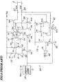
- An input/output circuit 10 shown in Fig. 5 comprises an output circuit 12 and an input circuit 14.
- the input/output circuit 10 comes in the input/output circuit 41 for example.
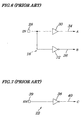
- An output circuit 12 comprises: an input-signal supply circuit 16 (see Fig. 6) which inputs input signals; a reference voltage source 18; a differential amplifier stage 20; an enabled/disable-state switching circuit 22 (see Fig. 7); a differential amplifier stage 24; and an output stage 26.
- the input circuit 14 comprises: a differential amplifier stage 42; an output stage 44; and a buffer B1.
- the n-channel type MOSFET N13 has its source connected to the ground potential. Also, the gate of the p-channel type MOSFET P3 and that of the p-channel type MOSFET P4 are interconnected, while the gate and the drain of the p-channel type MOSFET P4 are interconnected.
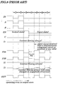
- a low-level voltage is output from the output terminal O1 of the differential amplifier stage 20 and a high-level voltage, from its output terminal O2.
- a low-level voltage from the enabled/disabled-state switching circuit 22 is applied to the n-channel type MOSFET N8 and N10 of the output stage 26 at their gate (period 1 ⁇ in Fig. 8-C), thereby turning these transistors off.
- a high-level voltage is applied to the p-channel type MOSFET at its gate, to reduce the conductivity of that MOKSFET P5, thus decreasing a current flowing through that MOSFET P5 (period 1 ⁇ in Fig. 8-I3) .
- Reduction in the conductivity of this MOSFET P5 causes a low-level voltage to be applied to the buffer B1.
- the buffer B1 then clamps thus applied low-level voltage to a low CMOS level.
- the low-level voltage thus clamped at a CMOS level is provided to the input circuit 14 at its output terminal OUT. Therefore, there is no possibility that a through current may flow through the CMOS transistors of the CMOS internal circuit.
- a gate of the n-channel type MOSFET N15 is connected to the make-and-break control-signal generating circuit 22A at its output terminal 41 and that of the n-channel type MOSFET N16, to the same circuit 22A at its output terminal 40.
- a first difference is that the reference voltage source 18 is provided as an output and also that the make-and-break control circuit 47 is provided between a gate of the n-channel type MOSFET N13 of the differential amplifier stage 42 and that of the n-channel type MOSFET N14 of the output stage 44.
- the make-and-break control circuit 47 consists of n-channel type MOSFETs N17 and N18.
- this embodiment is so configured that when the input circuit 14A is supplied with a high level of the Enable signal and not operating, from its output terminal to a CMOS internal circuit to which that output terminal is connected, a signal is supplied that represents a value expected at that CMOS internal circuit.
- an input circuit before receiving a data signal, surely receives a reconciliation signal called a data prefix, the logic of which is predefined in such a way that the first combination of the above-mentioned two combinations of signal logic always indicates "1" and the second combination, "0.”
- the n-channel type MOSFET N15 is turned off and the n-channel type MOSFET N16 is turned on.
- none of the n-channel type MOSFETs N3 and N6 operate as a current source. Therefore, no power is dissipated at the differential amplifier stage 20.
Landscapes
- Engineering & Computer Science (AREA)
- Power Engineering (AREA)
- Computer Networks & Wireless Communication (AREA)
- Signal Processing (AREA)
- Computer Hardware Design (AREA)
- Physics & Mathematics (AREA)
- Computing Systems (AREA)
- General Engineering & Computer Science (AREA)
- Mathematical Physics (AREA)
- Logic Circuits (AREA)
- Dc Digital Transmission (AREA)
- Small-Scale Networks (AREA)
Applications Claiming Priority (2)
| Application Number | Priority Date | Filing Date | Title |
|---|---|---|---|
| JP10353564A JP2000183719A (ja) | 1998-12-11 | 1998-12-11 | 入力回路、出力回路及び入出力回路、並びに該入出力回路を備えた信号伝送システム |
| JP35356498 | 1998-12-11 |
Publications (3)
| Publication Number | Publication Date |
|---|---|
| EP1009136A2 true EP1009136A2 (fr) | 2000-06-14 |
| EP1009136A3 EP1009136A3 (fr) | 2002-02-13 |
| EP1009136B1 EP1009136B1 (fr) | 2007-09-05 |
Family
ID=18431698
Family Applications (1)
| Application Number | Title | Priority Date | Filing Date |
|---|---|---|---|
| EP99124680A Expired - Lifetime EP1009136B1 (fr) | 1998-12-11 | 1999-12-10 | Source de courant réglé pour un circuit d'attaque de ligne et de réception |
Country Status (5)
| Country | Link |
|---|---|
| US (1) | US6366126B1 (fr) |
| EP (1) | EP1009136B1 (fr) |
| JP (1) | JP2000183719A (fr) |
| KR (1) | KR100360507B1 (fr) |
| DE (1) | DE69937034T2 (fr) |
Families Citing this family (6)
| Publication number | Priority date | Publication date | Assignee | Title |
|---|---|---|---|---|
| JP3423267B2 (ja) * | 2000-01-27 | 2003-07-07 | 寛治 大塚 | ドライバ回路、レシーバ回路、および信号伝送バスシステム |
| US7040520B2 (en) * | 2002-09-12 | 2006-05-09 | Illinois Tool Works Inc. | Fan motor suspension mount for a combustion-powered tool |
| JP2006235452A (ja) * | 2005-02-28 | 2006-09-07 | Sanyo Epson Imaging Devices Corp | 表示パネル駆動装置、表示装置、差動伝送システムおよび差動信号出力装置 |
| US7772875B2 (en) * | 2005-12-21 | 2010-08-10 | Nxp B.V. | Input/output circuit for evaluating delay |
| JP5109717B2 (ja) * | 2008-02-28 | 2012-12-26 | 日本電気株式会社 | 送信回路 |
| CN112398466A (zh) * | 2019-08-15 | 2021-02-23 | 成都锐成芯微科技股份有限公司 | 一种低压高速驱动电路 |
Family Cites Families (22)
| Publication number | Priority date | Publication date | Assignee | Title |
|---|---|---|---|---|
| JPS60143498A (ja) | 1983-12-29 | 1985-07-29 | Mitsubishi Electric Corp | 半導体入力回路 |
| JPS60252979A (ja) * | 1984-05-30 | 1985-12-13 | Oki Electric Ind Co Ltd | Cmos入出力回路 |
| JPS6218115A (ja) * | 1985-07-17 | 1987-01-27 | Oki Electric Ind Co Ltd | Cmos入出力回路 |
| US4697107A (en) * | 1986-07-24 | 1987-09-29 | National Semiconductor Corporation | Four-state I/O control circuit |
| US5248909A (en) * | 1990-01-09 | 1993-09-28 | Fujitsu Limited | ECL-TO-GaAs level converting circuit |
| JPH03270319A (ja) * | 1990-03-19 | 1991-12-02 | Fujitsu Ltd | レベル変換回路 |
| US5017813A (en) * | 1990-05-11 | 1991-05-21 | Actel Corporation | Input/output module with latches |
| JP2623374B2 (ja) * | 1991-02-07 | 1997-06-25 | ローム株式会社 | 出力回路 |
| JPH04256217A (ja) | 1991-02-08 | 1992-09-10 | Fujitsu Ltd | スリーステート型eclゲート |
| JPH0645909A (ja) | 1992-07-23 | 1994-02-18 | Mitsubishi Electric Corp | 双方向バッファ回路 |
| US5331220A (en) * | 1993-02-12 | 1994-07-19 | Xilinx, Inc. | Soft wakeup output buffer |
| US5521531A (en) * | 1993-12-13 | 1996-05-28 | Nec Corporation | CMOS bidirectional transceiver/translator operating between two power supplies of different voltages |
| US5469473A (en) * | 1994-04-15 | 1995-11-21 | Texas Instruments Incorporated | Transceiver circuit with transition detection |
| JPH08162942A (ja) * | 1994-11-29 | 1996-06-21 | Mitsubishi Electric Corp | 出力回路、入力回路、およびこれらを用いた入出力インタフェースシステム |
| JP3515235B2 (ja) | 1995-07-25 | 2004-04-05 | 富士通株式会社 | 半導体記憶装置 |
| US5736870A (en) * | 1995-12-28 | 1998-04-07 | Intel Corporation | Method and apparatus for bi-directional bus driver |
| US5644258A (en) * | 1996-01-04 | 1997-07-01 | Winbond Electronics Corp. | Driver circuit, with low idle power consumption, for an attachment unit interface |
| US5729547A (en) * | 1996-02-07 | 1998-03-17 | Dutec, Inc. | Automatic driver/receiver control for half-duplex serial networks |
| KR100199049B1 (ko) * | 1996-06-05 | 1999-06-15 | 윤종용 | Cmos 기준 전류원 회로 |
| JP3365468B2 (ja) * | 1996-06-17 | 2003-01-14 | 日本電信電話株式会社 | データ伝送回路 |
| US5729156A (en) * | 1996-06-18 | 1998-03-17 | Micron Technology | ECL to CMOS level translator using delayed feedback for high speed BiCMOS applications |
| US6014036A (en) * | 1997-11-20 | 2000-01-11 | International Business Machines Corporation | Bidirectional data transfer path having increased bandwidth |
-
1998
- 1998-12-11 JP JP10353564A patent/JP2000183719A/ja active Pending
-
1999
- 1999-12-10 KR KR1019990056468A patent/KR100360507B1/ko not_active Expired - Fee Related
- 1999-12-10 DE DE69937034T patent/DE69937034T2/de not_active Expired - Lifetime
- 1999-12-10 EP EP99124680A patent/EP1009136B1/fr not_active Expired - Lifetime
- 1999-12-10 US US09/458,055 patent/US6366126B1/en not_active Expired - Lifetime
Also Published As
| Publication number | Publication date |
|---|---|
| KR20000048068A (ko) | 2000-07-25 |
| JP2000183719A (ja) | 2000-06-30 |
| US6366126B1 (en) | 2002-04-02 |
| EP1009136B1 (fr) | 2007-09-05 |
| KR100360507B1 (ko) | 2002-11-13 |
| DE69937034D1 (de) | 2007-10-18 |
| EP1009136A3 (fr) | 2002-02-13 |
| DE69937034T2 (de) | 2008-05-29 |
Similar Documents
| Publication | Publication Date | Title |
|---|---|---|
| EP0475711B1 (fr) | Système pour transférer des données entre des puces de circuits intégrés | |
| JP3699764B2 (ja) | ドライバ回路装置及びインターフェース | |
| US5486782A (en) | Transmission line output driver | |
| US7940086B2 (en) | Interface circuit that can switch between single-ended transmission and differential transmission | |
| US7965121B2 (en) | Multifunctional output drivers and multifunctional transmitters using the same | |
| JP4814791B2 (ja) | レベル・シフター | |
| US7301371B2 (en) | Transmitter of a semiconductor device | |
| EP1011197B1 (fr) | Circuit pour générer des signaux différentiels à trois états et circuit différentiel à trois états | |
| US7733128B2 (en) | Transmitting apparatus | |
| JP4206731B2 (ja) | 送受信装置及びそれを備えた高速動作インタフェースシステム | |
| JPH07235952A (ja) | 信号伝送回路およびその回路を用いた信号伝送装置 | |
| US5436887A (en) | Digital full-duplex transceiver | |
| EP1009136B1 (fr) | Source de courant réglé pour un circuit d'attaque de ligne et de réception | |
| US5666068A (en) | GTL input receiver with hysteresis | |
| JP4582865B2 (ja) | 過電圧耐性を備えたバス・ホールド回路 | |
| JP4201202B2 (ja) | パス装置用低電圧変調回路 | |
| US7282958B2 (en) | Multiplex (MUX) circuit having a single selection signal and method of generating a MUX output signal with single selection signal | |
| US6741106B2 (en) | Programmable driver method and apparatus for high and low voltage operation | |
| JPH11154859A (ja) | 多値信号伝送方法および多値信号伝送システム並びに半導体集積回路 | |
| US5880606A (en) | Programmable driver circuit for multi-source buses | |
| US7126369B2 (en) | Transceiver providing high speed transmission signal using shared resources and reduced area | |
| US5942995A (en) | Return-to-zero receiver | |
| KR20030041759A (ko) | 고속동작 인터페이스를 위한 능동종단기 및 자체종단구동기를 포함하는 송수신 장치 및 시스템 | |
| JPH0846602A (ja) | 双方向性回路システム |
Legal Events
| Date | Code | Title | Description |
|---|---|---|---|
| PUAI | Public reference made under article 153(3) epc to a published international application that has entered the european phase |
Free format text: ORIGINAL CODE: 0009012 |
|
| AK | Designated contracting states |
Kind code of ref document: A2 Designated state(s): AT BE CH CY DE DK ES FI FR GB GR IE IT LI LU MC NL PT SE Kind code of ref document: A2 Designated state(s): DE FR GB |
|
| AX | Request for extension of the european patent |
Free format text: AL;LT;LV;MK;RO;SI |
|
| PUAL | Search report despatched |
Free format text: ORIGINAL CODE: 0009013 |
|
| AK | Designated contracting states |
Kind code of ref document: A3 Designated state(s): AT BE CH CY DE DK ES FI FR GB GR IE IT LI LU MC NL PT SE |
|
| AX | Request for extension of the european patent |
Free format text: AL;LT;LV;MK;RO;SI |
|
| RIC1 | Information provided on ipc code assigned before grant |
Free format text: 7H 04L 25/02 A, 7H 04L 5/14 B |
|
| 17P | Request for examination filed |
Effective date: 20020124 |
|
| AKX | Designation fees paid |
Free format text: DE FR GB |
|
| RAP1 | Party data changed (applicant data changed or rights of an application transferred) |
Owner name: NEC ELECTRONICS CORPORATION |
|
| 17Q | First examination report despatched |
Effective date: 20040406 |
|
| GRAP | Despatch of communication of intention to grant a patent |
Free format text: ORIGINAL CODE: EPIDOSNIGR1 |
|
| GRAS | Grant fee paid |
Free format text: ORIGINAL CODE: EPIDOSNIGR3 |
|
| GRAA | (expected) grant |
Free format text: ORIGINAL CODE: 0009210 |
|
| AK | Designated contracting states |
Kind code of ref document: B1 Designated state(s): DE FR GB |
|
| REG | Reference to a national code |
Ref country code: GB Ref legal event code: FG4D |
|
| REF | Corresponds to: |
Ref document number: 69937034 Country of ref document: DE Date of ref document: 20071018 Kind code of ref document: P |
|
| ET | Fr: translation filed | ||
| PLBE | No opposition filed within time limit |
Free format text: ORIGINAL CODE: 0009261 |
|
| STAA | Information on the status of an ep patent application or granted ep patent |
Free format text: STATUS: NO OPPOSITION FILED WITHIN TIME LIMIT |
|
| 26N | No opposition filed |
Effective date: 20080606 |
|
| PGFP | Annual fee paid to national office [announced via postgrant information from national office to epo] |
Ref country code: FR Payment date: 20081212 Year of fee payment: 10 |
|
| PGFP | Annual fee paid to national office [announced via postgrant information from national office to epo] |
Ref country code: GB Payment date: 20081210 Year of fee payment: 10 |
|
| GBPC | Gb: european patent ceased through non-payment of renewal fee |
Effective date: 20091210 |
|
| REG | Reference to a national code |
Ref country code: FR Ref legal event code: ST Effective date: 20100831 |
|
| PG25 | Lapsed in a contracting state [announced via postgrant information from national office to epo] |
Ref country code: FR Free format text: LAPSE BECAUSE OF NON-PAYMENT OF DUE FEES Effective date: 20091231 |
|
| PG25 | Lapsed in a contracting state [announced via postgrant information from national office to epo] |
Ref country code: GB Free format text: LAPSE BECAUSE OF NON-PAYMENT OF DUE FEES Effective date: 20091210 |
|
| REG | Reference to a national code |
Ref country code: DE Ref legal event code: R082 Ref document number: 69937034 Country of ref document: DE Representative=s name: GLAWE DELFS MOLL - PARTNERSCHAFT VON PATENT- U, DE |
|
| REG | Reference to a national code |
Ref country code: DE Ref legal event code: R082 Ref document number: 69937034 Country of ref document: DE Representative=s name: GLAWE DELFS MOLL PARTNERSCHAFT MBB VON PATENT-, DE Effective date: 20120828 Ref country code: DE Ref legal event code: R082 Ref document number: 69937034 Country of ref document: DE Representative=s name: GLAWE DELFS MOLL - PARTNERSCHAFT VON PATENT- U, DE Effective date: 20120828 Ref country code: DE Ref legal event code: R081 Ref document number: 69937034 Country of ref document: DE Owner name: RENESAS ELECTRONICS CORPORATION, KAWASAKI-SHI, JP Free format text: FORMER OWNER: NEC ELECTRONICS CORP., KAWASAKI, KANAGAWA, JP Effective date: 20120828 Ref country code: DE Ref legal event code: R081 Ref document number: 69937034 Country of ref document: DE Owner name: RENESAS ELECTRONICS CORPORATION, JP Free format text: FORMER OWNER: NEC ELECTRONICS CORP., KAWASAKI, JP Effective date: 20120828 |
|
| PGFP | Annual fee paid to national office [announced via postgrant information from national office to epo] |
Ref country code: DE Payment date: 20140602 Year of fee payment: 15 |
|
| REG | Reference to a national code |
Ref country code: DE Ref legal event code: R119 Ref document number: 69937034 Country of ref document: DE |
|
| PG25 | Lapsed in a contracting state [announced via postgrant information from national office to epo] |
Ref country code: DE Free format text: LAPSE BECAUSE OF NON-PAYMENT OF DUE FEES Effective date: 20150701 |