EP1020933A1 - Photocoupleur, son procédé de fabrication et cadre conducteur pour un photocoupleur - Google Patents
Photocoupleur, son procédé de fabrication et cadre conducteur pour un photocoupleur Download PDFInfo
- Publication number
- EP1020933A1 EP1020933A1 EP00100502A EP00100502A EP1020933A1 EP 1020933 A1 EP1020933 A1 EP 1020933A1 EP 00100502 A EP00100502 A EP 00100502A EP 00100502 A EP00100502 A EP 00100502A EP 1020933 A1 EP1020933 A1 EP 1020933A1
- Authority
- EP
- European Patent Office
- Prior art keywords
- lead frame
- light emitting
- photodetector
- output
- emitting element
- Prior art date
- Legal status (The legal status is an assumption and is not a legal conclusion. Google has not performed a legal analysis and makes no representation as to the accuracy of the status listed.)
- Granted
Links
Images


Classifications
-
- H—ELECTRICITY
- H10—SEMICONDUCTOR DEVICES; ELECTRIC SOLID-STATE DEVICES NOT OTHERWISE PROVIDED FOR
- H10F—INORGANIC SEMICONDUCTOR DEVICES SENSITIVE TO INFRARED RADIATION, LIGHT, ELECTROMAGNETIC RADIATION OF SHORTER WAVELENGTH OR CORPUSCULAR RADIATION
- H10F55/00—Radiation-sensitive semiconductor devices covered by groups H10F10/00, H10F19/00 or H10F30/00 being structurally associated with electric light sources and electrically or optically coupled thereto
- H10F55/20—Radiation-sensitive semiconductor devices covered by groups H10F10/00, H10F19/00 or H10F30/00 being structurally associated with electric light sources and electrically or optically coupled thereto wherein the electric light source controls the radiation-sensitive semiconductor devices, e.g. optocouplers
- H10F55/25—Radiation-sensitive semiconductor devices covered by groups H10F10/00, H10F19/00 or H10F30/00 being structurally associated with electric light sources and electrically or optically coupled thereto wherein the electric light source controls the radiation-sensitive semiconductor devices, e.g. optocouplers wherein the radiation-sensitive devices and the electric light source are all semiconductor devices
-
- H—ELECTRICITY
- H10—SEMICONDUCTOR DEVICES; ELECTRIC SOLID-STATE DEVICES NOT OTHERWISE PROVIDED FOR
- H10W—GENERIC PACKAGES, INTERCONNECTIONS, CONNECTORS OR OTHER CONSTRUCTIONAL DETAILS OF DEVICES COVERED BY CLASS H10
- H10W72/00—Interconnections or connectors in packages
- H10W72/50—Bond wires
- H10W72/551—Materials of bond wires
- H10W72/552—Materials of bond wires comprising metals or metalloids, e.g. silver
- H10W72/5522—Materials of bond wires comprising metals or metalloids, e.g. silver comprising gold [Au]
-
- H—ELECTRICITY
- H10—SEMICONDUCTOR DEVICES; ELECTRIC SOLID-STATE DEVICES NOT OTHERWISE PROVIDED FOR
- H10W—GENERIC PACKAGES, INTERCONNECTIONS, CONNECTORS OR OTHER CONSTRUCTIONAL DETAILS OF DEVICES COVERED BY CLASS H10
- H10W90/00—Package configurations
-
- H—ELECTRICITY
- H10—SEMICONDUCTOR DEVICES; ELECTRIC SOLID-STATE DEVICES NOT OTHERWISE PROVIDED FOR
- H10W—GENERIC PACKAGES, INTERCONNECTIONS, CONNECTORS OR OTHER CONSTRUCTIONAL DETAILS OF DEVICES COVERED BY CLASS H10
- H10W90/00—Package configurations
- H10W90/701—Package configurations characterised by the relative positions of pads or connectors relative to package parts
- H10W90/751—Package configurations characterised by the relative positions of pads or connectors relative to package parts of bond wires
- H10W90/756—Package configurations characterised by the relative positions of pads or connectors relative to package parts of bond wires between a chip and a stacked lead frame, conducting package substrate or heat sink
Definitions
- the present invention relates to a photocoupler device integrally including a light emitting element, and an output photodetector and a monitor photodetector for receiving light emitted by the light emitting element.
- the present invention also relates to a fabrication method thereof.
- the present invention relates to a lead frame for the photocoupler device.
- an optical signal is transmitted from a light emitting element on a primary side to a photodetector on a secondary side while the primary side and the secondary side are electrically isolated from each other.
- the light emitting element and the photodetector are mounted on a lead frame, an optical path therebetween is made of a light-transmissive resin, and the optical path is covered with a light-shielding resin.
- a photocoupler device including two photodetectors, one for signal transmission and the other for monitoring, has been proposed. Specifically, an extra photodetector is provided on the primary side in order to monitor an emission output level of the light emitting element, and to feed the monitoring result back to the light emitting element. This solves the problem of nonlinearity in temperature characteristics, etc., which is specific to light emitting elements, thereby stabilizing the emission output level.
- Figure 10 is a plan view showing one example of the conventional photocoupler device.
- Figure 11 is a cross-sectional view of the photocoupler device shown in Figure 10 .
- a light emitting element 101 is mounted on a primary side lead frame 102a via an electrically conductive paste or the like, and connected to a lead frame 103 for connecting a line by an Au wire 104 or the like.
- An output photodetector 105 is mounted on a secondary side lead frame 102b , and is connected to a lead frame 106 for connecting a line by an Au wire 104 or the like.
- a photodetector 107 for monitoring (hereinafter, referred to as “monitor photodetector 107 ”) is mounted on the primary side lead frame 102a in the same manner as the light emitting element 101 , and connected to a lead frame 108 for connecting a line by the Au wire 104 or the like.
- the light emitting element 101 , the output photodetector 105 , and the monitor photodetector 107 are placed on the same plane, and are covered with a light-transmissive resin layer 109 which is made of a transmissive potting resin such as a silicone resin. Additionally, the resultant structure is covered with a molded layer 110 made of a light-shielding resin such as an epoxy resin, in order to reflect an optical signal from the light emitting element 101 and/or block interfering stray light from outside.
- a light-transmissive resin layer 109 which is made of a transmissive potting resin such as a silicone resin.
- the resultant structure is covered with a molded layer 110 made of a light-shielding resin such as an epoxy resin, in order to reflect an optical signal from the light emitting element 101 and/or block interfering stray light from outside.
- Figure 12 is a schematic circuit diagram of the photocoupler device including the light emitting element 101 , the output photodetector 105 , and the monitor photodetector 107 , which are electrically isolated from one another. Between the light emitting element 101 and the photodetector 105 , and between the light emitting element 101 and the photodetector 107 , only optical signals are transmitted.
- the light emitting element 101 upon receiving an electric signal through the lead frame 103 for connecting a line, the light emitting element 101 photoelectrically converts the electric signal to an optical signal, and emits the optical signal.
- the optical signal travels through the light-transmissive resin layer 109 and is reflected by the interface between the light-transmissive resin layer 109 and the molded layer 110 .
- the reflected optical signal reaches the output photodetector 105 and the monitor photodetector 107 .
- the output photodetector 105 converts the optical signal to an electric signal, and outputs the electric signal.
- the monitor photodetector 107 converts the optical signal to an electric signal, and outputs the electric signal.
- the electric signal from the monitor photodetector 107 is fed back in order to control an emitting operation of the light emitting element 101.
- FIG 17 is a circuit diagram showing a configuration example of a high-linearity analogue photocoupler device (hereinafter, simply referred to as a "linear photocoupler"). Although not shown, two devices are required for the substitution of pulse transes. Thus, a majority of linear photocoupler devices include two channels of devices in one package.
- a typical linear photocoupler includes a light emitting element (LED) 202 and a monitor output element (photodiode) 203 on a primary side, and an output element (photodiode) 204 on a secondary side.
- LED light emitting element
- photodiode monitor output element
- IPD1 and IPD2 photoelectric currents flowing through the monitor output element 203 and the output element 204
- a typical photocoupler includes the light emitting element 202 , the monitor photodetector 203 , which is used for stabilizing the emission of the light emitting element 202 , on the primary side and the output photodetector 204 on the secondary side.
- the same level of light from the light emitting element 202 is incident on each of the two photodetector 203 and 204 , and that the primary side and the secondary side are electrically isolated from each other.
- a light emitting element 202, a monitor output photodetector 203, and an output photodetector 204 are die-bonded (adhered) onto a flat lead frame 201 .
- the elements are covered with a transparent silicone resin 206 or the like, and then transfer-molded with an epoxy resin 207 .
- Figure 19 an example of the structure of the lead frames
- Figure 20 a cross sectional view of an example of a photocoupler
- lead frames 201 and 201 ' are used.
- a tip of the lead frame 201 is raised upward and provided with only the light emitting element 202 adhered and mounted thereon, while a tip of the lead frame 201' is lowered and provided with a photodetector 203 for monitoring and a photodetector 204 for output adhered and mounted thereon.
- Each element is wire bonded to the outer leads, respectively, as shown in the drawings.
- the light emitting element 202 is precoated with a transparent silicone resin 208 for relieving the stress thereof, and then positioned over the photodetector 203 for monitoring and the photodetector for output 204 so as to face the photodetectors 203 and 204 .
- the first transfer molding process is performed with a light-transmissive epoxy resin 209 and, in addition, the second transfer molding process is performed with a light-shielding epoxy resin 210 , resulting in the structure shown in Figure 20 .
- the ratio of the output level between the monitor photodetector and the output photodetector, and the stability thereof are essential characteristics.
- various ideas and considerable efforts has been directed to the formation of the light-transmissive resin layer, i.e., the optical path which affects the ratio of output level between the photodetectors.
- the shape of the light-transmissive resin layer can be stabilized.
- the shape of the light-transmissive resin layer can be stabilized.
- the shape of the light-transmissive resin layer is stabilized by using a surface tension of the silicone resin caused by the shape of the Au wire or the like connecting the elements to the lead frame.
- a surface tension of the silicone resin caused by the shape of the Au wire or the like connecting the elements to the lead frame.
- the state of the interface therebetween is unstable against the temperature variation, and the state of reflection on the interface is also unstable.
- temperature variation changes the transmission efficiency of optical signals between the light emitting element and each of the photodetectors. Consequently, reliability of the feed back control based on the output from the photodetector for monitoring is degraded.
- the photocoupler device since the optical signal travels by using reflection, a white resin with less fillers has been typically used for the outer molded layer. Accordingly, the photocoupler device is likely to be affected by interfering stray light from outside, and thus has less reliability.
- characteristics of the element are likely to vary due to the temperature fluctuation around the element (caused by reflow, soldering, etc.). Specifically, because of heat in the interface between the silicone resin 206 covering the elements 202, 203 , and 204 and the epoxy resin 207 , the silicone resin 206 and the epoxy resin 207 are peeled off from or adhered to each other at the interface therebetween. This affects the reflection of light from the light emitting element 202 , and therefore causes light-transmission efficiency from the element 202 to the monitor output element 203 and the output element 204 to be varied. In addition, the withstand voltage between the primary and secondary sides is inferior to that of the dual-transfer type photocoupler shown in Figures 19 and 20 .
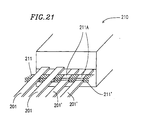
- a tie bar portion 211 is superposed on another tie bar portion 211' .
- Such unnecessary portions (shaded portions) of the tie bar 211 are cut off by a metal mold after being covered with light-shielding epoxy resin 210.
- more pressure is required as compared with the case where single tie bar (having 1/2 the thickness of the shaded portion) is cut off.
- portions 211A of the tie bar 211 are not cut away and therefore remain on the leads. These remainders may be left in the mold unless manually removed. This may cause troubles such as breakage of the mold. When the remainders are manually removed, productivity significantly decreases.
- the conventional photocoupler device bears various complicated problems as to characteristics, a structure, and productivity thereof.
- it has been required to devise a photocoupler having a novel structure.
- a photocoupler device includes a light emitting element; a monitor photodetector and an output photodetector for receiving light from the light emitting element; a primary side lead frame for mounting the light emitting element and the monitor photodetector; and a secondary side lead frame for mounting the output photodetector, wherein the light emitting element and the output photodetector are placed so as to face each other.
- the monitor photodetector on the primary side lead frame and the output photodetector on the secondary side lead frame are provided on a same plane, and are positioned so as to face the light emitting element on the primary side lead frame.
- the monitor photodetector and the light emitting element on the primary side lead frame are provided on a same plane, and are positioned so as to face the output photodetector on the secondary side lead frame.
- the monitor photodetector and the light emitting element of the primary side lead frame are positioned at different levels, and face the output photodetector on the secondary side lead frame.
- the light emitting element, the monitor photodetector, and the output photodetector are covered with a light-transmissive resin through a first transfer molding process, and then, are further covered with a light-shielding resin through a second transfer molding process.
- the light emitting element and the monitor photodetector, or the light emitting element and the output photodetector are covered with a single transparent resin layer.
- At least one of the light emitting element, the monitor photodetector, and the output photodetector is precoated with a transparent resin layer.
- a method for fabricating a photocoupler device including a light emitting element, and a monitor photodetector and an output photodetector for receiving light from the light emitting element includes steps of: mounting the light emitting element on a first lead frame; mounting the output photodetector and the monitor photodetector on a second lead frame; and combining the first lead frame and the second lead frame so that the light emitting element and the monitor photodetector are provided on a primary side, and the output photodetector is provided on a secondary side.
- a lead frame for a photocoupler device includes a primary side lead frame and a secondary side lead frame, wherein the primary side lead frame and the secondary side lead frame are combined together, and have a common reference plane, wherein the primary and secondary side lead frames each have a plurality of turned-up portions extending upward with respect to the reference plane, and a plurality of turned-down portions extending downward with respect to the reference plane, and one of the turned-up portions does not extend over any other turned-up portion, and one of the turned-down portions does not extend below any other turned-down portion.
- element-pairs of a light emitting element and a monitor output element, and output elements are provided one after another on each of the primary and secondary side lead frames; and the primary and secondary side lead frames are assembled so that one of the element-pairs provided on the primary side lead frame faces corresponding one of the output elements provided on the secondary side lead frame, and one of the element-pairs provided on the secondary side lead frame faces corresponding one of the output elements provided on the primary side lead frame.
- a photocoupler device includes a light emitting element; a monitor output element; an output element; and a primary side lead frame and a secondary side lead frame having a common reference plane, wherein the primary and secondary side lead frames each have a plurality of element mounting portions for alternately mounting the light emitting element, the monitor output element, and the output element, wherein some of the plurality of element mounting portions extend upward and others extend downward with respect to the reference plane, and wherein one of the element mounting portions extending upward does not extend over any other element mounting portion extending upward, and one of the element mounting portions extending downward does not extend below any other element mounting portion extending downward, and the primary and secondary side lead frames are assembled so that one of pairs of the light emitting element and the monitor output element provided on the primary side lead frame faces corresponding one of the output elements provided on the secondary side lead frame, and one of pairs of the light emitting element and the monitor output element provided on the secondary side lead frame faces corresponding one of the output elements provided on the primary side lead frame.
- the light emitting element 12 upon receiving an electric signal via the lead frame 17 for connecting a line, the light emitting element 12 photoelectrically converts the electric signal to an optical signal, and outputs the optical signal.
- the optical signal travels through the light-transmissive resin 22 and reaches the output photodetector 15 and the monitor photodetector 13 .
- the output photodetector 15 converts the optical signal to an electric signal, and outputs the electric signal via the lead frame 19 for connecting a line.
- the monitor photodetector 13 converts the optical signal to an electric signal, and outputs the electric signal via the lead frame 18 for connecting a line.
- the electric signal from the monitor photodetector 13 is fed back in order to control the output operation of the light emitting element 12. Since the light emitting element 12 is placed so as to face the monitor photodetector 13 and the output photodetector 15 , both of the optical paths between the light emitting element 12 and the photodetector 13 , and between the light emitting element 12 and the photodetector 15 are linear.
- the primary and secondary side lead frames 231 and 232 are combined into a laminate, and have the same reference plane when they are combined.
- the lead frames 231 and 232 are provided with element mounting portions 212-217 and 218-223 , respectively, and turned-up or turned-down with respect to the reference plane.
- One of the element mounting portions extending upward does not extend over any other element mounting portion extending upward, and one of the element mounting portions extending downward does not extend below any other element mounting portion extending downward.
- a light emitting element 202 On the element mounting portions of each of the primary and secondary side lead frames, a light emitting element 202 , a monitor output element 203 and an output element 204 are placed in alternate order.
- an element pair including the light emitting element and the monitor output element on the primary side faces the output element on the secondary side
- an element pair including the light emitting element and the monitor output element on the secondary side faces the output element on the primary side.
- a light emitting element and an output photodetector are placed so as to be face each other.
- an optical path between the light emitting element and the output photodetector becomes linear, whereby light emitted by the light emitting element is directly incident on the output photodetector.
- effects of the optical path on the optical signals are small.
- the optical path is linear and short, and expensive silicone resin is not required for the formation of the optical path. Even if the silicone resin is used, a paltry amount of silicone resin is sufficient. Additionally, since the optical signal travels without using reflection, the optical signal is not likely to be affected by the external shape of the optical path.
- an output ratio between the monitor photodetector and the output photodetector becomes stable. Furthermore, a transmission efficiency of the optical signal between the light emitting element and the photodetector does not vary even when the state of the reflection surface is varied due to the temperature variation because the optical signal travels without using reflection. Furthermore, for the same reason, a light-shielding resin, e.g., a resin of black color, can be applied to the outermost surface of the photocoupler device, whereby interfering stray light from outside is surely blocked. As a result, reliability of the photocoupler device can be increased.
- a light-shielding resin e.g., a resin of black color
- a light emitting element is mounted on the primary side lead frame, while the monitor photodetector and the output photodetector are mounted on the secondary side lead frame.
- the lead frames are combined so as to provide a light emitting element and a monitor photodetector on the primary side and the output photodetector on the secondary side.
- the light emitting element and respective photodetectors can be separately assembled. If assemblies of the elements are concurrently conducted, the fabrication process is simplified. After the lead frames are combined, the light emitting element and the monitor photodetector belong to the primary side, while the output photodetector belongs to the secondary side. This arrangement causes no problem in practical use.
- the invention described herein makes possible the advantages of (1) providing a photocoupler device with a stable output ratio between photodetectors and a high reliability, and a fabrication method of the photocoupler device, and (2) providing a lead frame with a simple structure, superior characteristics, and improved productivity, and a photocoupler device using the same.
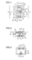
- Figure 1 is a plan view showing one embodiment of a photocoupler device according to the present invention.
- Figure 2 is a cross-sectional view of the photocoupler device taken along line A-A' of Figure 1 .
- Figure 3 is a cross-sectional view of the photocoupler device taken along line B-B' of Figure 1 .
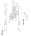
- Figures 4A and 4B show a plan view and a cross-sectional view of a first lead frame, respectively.
- Figures 5A and 5B show a plan view and a cross-sectional view of a second lead frame, respectively.
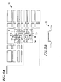
- Figure 6 is a plan view showing the first and second lead frames combined with each other.
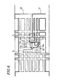
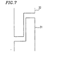
- Figure 7 is an enlarged plan view showing another combination of the first and second lead frames.
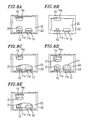
- Figures 8A-8E are cross-sectional views each showing a variation of a photocoupler device according to the present invention.
- Figures 9A-9C are cross-sectional views each showing another variation of a photocoupler device according to the present invention.
- Figure 10 is a plan view showing one example of the conventional photocoupler device.
- Figure 11 is a schematic front view of the conventional photocoupler device shown in Figure 10 .
- Figure 12 is a circuit configuration of the conventional photocoupler device shown in Figure 10.
- Figures 13A and 13B shows a plan view and a front view of a primary side lead frame, respectively.
- Figures 14A and 14B shows a plan view and a front view of a secondary side lead frame, respectively.
- Figure 15 is a plan view showing the primary and secondary side lead frames combined with each other.
- Figure 16 is a plan view showing an example of a structure of a photocoupler.
- Figure 17 shows an exemplary circuit configuration of a linear photocoupler.
- Figures 18A and 18B show a structure example of the conventional linear photocoupler.
- Figure 19 shows another structure example of the conventional linear photocoupler.
- Figure 20 is a cross-sectional view of the conventional linear photocoupler shown in Figure 19 .
- Figure 21 is a perspective view of the conventional linear photocoupler.
- Figure 1 is a plan view showing a photocoupler device according to one embodiment of the present invention.
- Figures 2 and 3 show cross-sectional views of the photocoupler device taken along line A-A' and line B-B' of Figure 1 , respectively.
- a light emitting element 12 and a photodetector for monitoring 13 are mounted on headers 11a and 11b of a primary side lead frame 11 , respectively; a photodetector for outputting 15 (hereinafter, referred to as “output photodetector 15" ) is mounted on a header 14a of a secondary side lead frame 14 .
- the header 11b and the header 14a are on the same plane, and the header 11a is on a different level.
- the light emitting element 12 is placed so as to face both of the monitor photodetector 13 and the output photodetector 15 .
- the light emitting element 12 is connected to a lead frame 17 for connecting a line by an Au wire 16 or the like.
- the monitor photodetector 13 is connected to a lead frame 18 for connecting a line by an Au wire 16 or the like.
- the output photodetector 15 is connected to a lead frame 19 for connecting a line by an Au wire 16 or the like.
- the light emitting element 12 is precoated with a transparent silicone resin 21 .
- the light emitting element 12 , the monitor photodetector 13 , and the output photodetector 15 are covered with a light-transmissive resin layer 22 .
- the light-transmissive resin layer 22 is covered with a light-shielding resin layer 23 .
- the photocoupler device has a circuit configuration similar to that shown in Figure 12 . As shown in Figure 12 , the light emitting element 12 , the monitor photodetector 13 , and the output photodetector 15 are electrically isolated from one another. Only optical signals are transmitted among the elements 12, 13 , and 15.
- the light emitting element 12 upon receiving an electric signal via the lead frame 17 for connecting a line, the light emitting element 12 photoelectrically converts the electric signal to an optical signal, and outputs the optical signal.
- the optical signal travels through the light-transmissive resin layer 22 and reaches the output photodetector 15 and the monitor photodetector 13.
- the output photodetector 15 converts the optical signal to an electric signal, and outputs the electric signal via the lead frame 19 for connecting a line.
- the monitor photodetector 13 converts the optical signal to an electric signal, and outputs the electric signal via the lead frame 18 for connecting a line.
- the electric signal from the monitor photodetector 13 is fed back in order to control an output operation of the light emitting element 12 .
- the light emitting element 12 is placed so as to face the monitor photodetector 13 and the output photodetector 15 , and is positioned in a position opposite to an area intermediate to the photodetectors 13 and 15 .
- the level of the signal received by the photodetector 13 and the level of the signal received by the photodetector 15 are substantially the same. Accordingly, the output levels from the photodetectors 13 and 15 are also substantially the same.
- Optical paths between the light emitting element 12 and the monitor photodetector 13 and between the light emitting element 12 and the output photodetector 15 both are linear.
- an output ratio between the monitor photodetector 13 and the output photodetector 15 does not change.
- it is not necessary to strictly define the shape and size of the light-transmissive resin layer 22 it is not required to use an expensive silicone resin for the light-transmissive resin layer 22 in order to stabilize the shape thereof. This avoids the increase in cost.
- silicone resin even when the silicone resin is used, amount of the silicone resin to be used is reduced by limiting the area to which the silicone resin is applied to small areas between the light emitting element 12 and the monitor photodetector 13 and between the light emitting element 12 and the output photodetector 15 . This suppresses the increase in cost.
- the present embodiment does not utilize the reflection of optical signals at an interface between a light-transmissive resin layer 22 and a light-shielding resin layer 23 .
- transmission efficiencies between the light emitting element 12 and the monitor photodetector 13 and between the light emitting element 12 and the output photodetector 15 do not vary. Accordingly, the output ratio between the monitor photodetector 13 and the output photodetector 15 does not change. As a result, feedback control based on the output of the monitor photodetector 13 can be effectively performed.
- a light-shielding resin which is of, e.g., a black color, can be used as the light-shielding resin layer 23 .
- the light-shielding resin layer 23 blocks substantially all interfering stray light from outside. Accordingly, reliability of the photocoupler device can be increased.
- Figures 4A and 4B shows a plan view and a cross-sectional view of a first lead frame 31 , respectively.
- Figures 5A and 5B shows a plan view and a cross-sectional view of a second lead frame 32 , respectively.
- the first lead frame 31 has the header 11a for mounting the light emitting element 12 , the lead frame 17 for connection with the light emitting element 12 , and the like. After the assembly of the entire lead frame structure has been completed, the first lead frame 31 functions as a part of the primary side lead frame 11 as shown in Figure 1 .
- the light emitting element 12 is adhered on the header 11a via an Ag paste and the like, and on the other hand is connected to the lead frame 17 for connecting a line by a bonding wire such as an Au wire 16 or the like. Thereafter, a precoating with a silicone resin layer 21 (not shown) is applied to the light emitting element 12 .
- the second lead frame 32 has the headers 11b and 14a , the lead frames 18 and 19 for connecting the photodetectors 13 and 15 . After the assembly of the entire lead frame structure has been completed, the second lead frame 32 functions as the primary side lead frame 11 and the secondary side lead frame 14 as shown in Figure 1 .
- the monitor photodetectors 13 and the output photodetector 15 are adhered on the headers 11b and 14a , respectively, via an Ag paste and the like, and on the other hand respectively are connected to the lead frames 18 and 19 for connecting a line by a bonding wire such as an Au wire 16.
- the process of mounting and wiring the light emitting element 12 onto the first lead frame 31 is performed independent of the process of mounting and wiring the photodetectors 13 and 15 onto the second lead frame 32 .
- these processes can be concurrently performed, and therefore can be simplified.
- the fabrication process becomes complicated because a face of the lead frame on which the light emitting element is mounted, is opposite to a face on which the photodetector is mounted.
- the second lead frame 32 is turned upside down so that the right side is replaced by the left side, and superposed on the first lead frame 31 , as shown in Figure 6 .
- the first lead frame 31 is depicted with thick lines
- the second lead frame 32 is depicted with thin lines.
- a light-transmissive resin layer 22 is formed by a first transfer molding so as to cover the light emitting element 12 , the monitor photodetectors 13 , and the output photodetector 15 (first transfer molding process). Furthermore, a light-shielding resin layer 23 is formed by a second transfer molding so as to cover the light-transmissive resin layer 22 (second transfer molding process).
- the molding resin leaks out from a portion C ( Figure 6 ) on the primary side between the first and second lead frames 31 and 32 during the molding processes.
- a pair of fitting portions e.g., a concavity and a convexity, are provided on each of the portions of upper and lower metal molds corresponding to the portion C in order to squash the portion C between the first and second lead frames 31 and 32 , thereby preventing the resin from leaking out therefrom.
- a pair of fitting portions e.g., a concavity and a convexity
- each of the elements are provided with sufficient protection and therefore the reliability thereof improves.
- a portion D ( Figure 6 ) of the first and second lead frames 31 and 32 is carved out to form the primary side lead frame 11 and the secondary side lead frame 14 as shown in Figure 1 , obtaining a photocoupler device.
- the primary side lead frame 11 is provided with the light emitting element 12 and the monitor photodetector 13, while the secondary side lead frame 14 is provided with the output photodetector 15 .
- FIGS 8A-8E show variations of the photocoupler device according to the present invention.
- the light emitting element 12 and the monitor photodetector 13 on the primary side lead frame 11 are provided on the same plane.
- the output photodetector 15 on the secondary side lead frame 14 faces the light emitting element 12 .
- the shape of the first and second lead frames can be simplified.
- the output photodetector 15 directly receives an optical signal from the light emitting element 12
- the monitor photodetector 13 mainly receives light reflected by the interface between the light-transmissive resin layer 22 and the light-shielding resin layer 23 causing a difference between the output level of the photodetector 15 and the output level of the photodetector 13 .
- a circuit constant e.g., resistance value
- each of the photodetectors 13 and 15 by precoating each of the photodetectors 13 and 15 with the silicone resin layer 21 as well as the light emitting element 12 as shown in Figure 8D, the transmission efficiency in each of the optical paths from the light emitting element 12 to the photodetectors 13 and 15 improves. Consequently, the output level from each of the photodetectors 13 and 15 is enhanced. That is, the transparency of the silicone resin layer 21 can be set to be higher than that of the light-transmissive resin layer 22 which is provided through the transfer molding process, whereby the transparency of some portions in the optical paths improves. As a result, transmission efficiency in each of the optical paths is increased, and the output level of each of the photodetectors 13 and 15 enhances.
- the light emitting element 12 and the output photodetector 15 may be covered with a single silicone resin layer 21 , thereby enhancing the output level from the output photodetector 15 .
- FIGS 9A-9C show another group of variations of the photocoupler device according to the present embodiment.
- the light emitting element 12 and the monitor photodetector 13 of the primary side lead frame 11 are positioned at different levels, i.e., the monitor photodetector 13 is positioned at the lower level than the light emitting element 12 .
- the light emitting element 12 is placed so as to face the output photodetector 15 of the secondary side lead frame 14 .
- each of the photodetectors 13 and 15 with the silicone resin layers 21 , respectively, as well as the light emitting element 12 as shown in Figure 9B, the transmission efficiency in each of the optical paths from the light emitting element 12 to the photodetectors 13 and 15 improves. Consequently, the output level from each of the photodetectors 13 and 15 is enhanced.
- the present invention provides lead frames wherein each of the primary and secondary side lead frames both have turned-up portions and turned-down portions for mounting light emitting elements and photodetectors.
- the light emitting elements and the photodetectors are provided so that light emitted by the light emitting element is incident directly on the photodetectors.
- variation in optical characteristics such as light-transmission efficiency does not occur.
- the present invention also provides a lead frame wherein unnecessary tie bar portions are not left on the leads when the lead frames are combined.
- the present invention further provides a photocoupler device using the lead frame.
- the photocoupler device of the present invention exhibits higher performance and reliability as compared with the conventional linear photocoupler.
- the photocoupler device of the present invention can be fabricated in a stable manner.
- reference plane of the lead frame used herein refers to a face of the substrate on which elements are provided.
- Figures 13A and 13B shows a plan view and a front view of a primary side lead frame, respectively.
- Figures 14A and 14B shows a plan view and a front view of a secondary side lead frame, respectively.
- a lead frame which can be used for a dual-channel type linear photocoupler is employed.
- a primary side lead frame 231 has cradles 233 and 234
- a secondary side lead frame 232 has cradles 235 and 236 in both sides thereof, respectively, on which the lead frames 231 and 232 are supported. These cradles facilitate the handling of the lead frames 231 and 232 .
- element-pairs of a light emitting element 202 (not shown) and a monitor output element 203 (not shown), and output elements 204 (not shown) are provided in alternate order.
- the primary side and secondary side lead frames 231 and 232 each have pulled-up portions and pulled-down portions for mounting a light emitting element 202 , a monitor output element 203 , and an output elements 204 .
- the pulled-up portions and pulled-down portions are formed so that the element-pair of the light emitting element 202 and the monitor output element 203 and the output elements 204 face each other when the primary side and secondary side lead frames 231 and 232 are combined.
- an element-pair of a light emitting element 202 and a monitor output element 203 of the primary side faces a corresponding output element 204 of the secondary side
- a pair of a light emitting element 202 and a monitor output element 203 of the secondary side faces corresponding output element 204 of the primary side.
- a header 212 and a terminal 213 of the primary side for mounting the light emitting element 202 are turned upward, in order to mount the light emitting element 202 on the back surface of the lead frame.
- a header 214 and a terminal 215 for mounting the monitor output element 203 , a header 216 and a terminal 217 for mounting the output element 204 are turned downward, in order to mount the monitor output element 203 and the output element 204 on the front surface of the lead frame.
- two sets of these elements and terminals are formed between the cradles 233 and 234 of the primary side lead frame 231 .
- leads of the secondary side lead frame 232 extend in a direction opposite to the direction to which the leads of the primary side lead frame 231 extend.
- a header 218 and a terminal 219 for mounting the light emitting element 202 are turned upward, in order to mount the light emitting element 202 on the back surface of the lead frame.
- a header 220 and a terminal 221 for mounting the monitor output element 203 , a header 222 and a terminal 223 for mounting the output element 204 are turned downward, in order to mount the monitor output element 203 and the output element 204 on the front surface of the lead frame.
- two sets of these elements and terminals are formed between the cradles 235 and 236 of the secondary side lead frame 232 .
- Figure 15 shows the primary side lead frame 231 and the secondary side lead frame 232 when they are combined.
- the cradles 233 and 234 of the primary side lead frame 231 has notches 238 (shown in Figure 13A ) for engaging with a tie bar 237 (shown in Figure 14A ), or the like, of the secondary side lead frame 232 so that the primary side lead frame 231 is accurately positioned with respect to the secondary side lead frame 232 when combined with the secondary side lead frame 232 .
- the secondary side lead frame 232 is bent downward along the horizontal direction of Figure 14A so that the primary and secondary side lead frames 231 and 232 have the same reference plane when they are combined into a laminate. (See Figures 13A, 13B, 14A , and 14B ).
- Figure 16 shows a structure of a photocoupler device using the lead frames 231 and 232 .
- the primary and secondary side lead frames 231 and 232 are combined as described above, thereby forming two dual-channel type linear photocouplers, which are denoted by reference numerals 239 and 240 .
- a pair formed by the light emitting element 202 (on the header 212 ) and the monitor output element 203 (on the header 214 ) of the primary side lead frame 231 , and the output element 204 (on the header 222 ) of the secondary side lead frame 232 constitute a channel 239A .
- the output element 204 (on the header 217 ) of the primary side lead frame 231 , and a pair formed by the light emitting element 202 (on the header 218 ) and the monitor output element 203 (on the header 220 ) of the secondary side lead frame 232 constitute another channel 239B .
- the channels 239A and 239B may be covered with a light-transmissive resin (first molding process), and the molded structure may be further covered with a light-shielding resin (second molding process).
- the precoat of the transparent silicone resin on the monitor output element and the output element is also effective for increasing the output current as much as possible.
- the present invention is also applicable to a single-channel type linear photocoupler, as described above.
- a light emitting element and an output photodetector are positioned so as to face each other.
- an optical path between the light emitting element and the output photodetector becomes linear, whereby light emitted by the light emitting element is directly incident on the output photodetector.
- effects of the optical path on optical signals are small.
- the optical path is linear and short, expensive silicone resin is not required for the formation of the optical path. Even if the silicone resin is used, a small amount of silicone resin is sufficient. Additionally, since the optical signal travels without using reflection, the optical signal is not likely to be affected by the external shape of the optical path.
- the transmission efficiency of the optical signal from the light emitting element to each of the photodetectors does not vary even when the state of the reflection surface is varied due to a temperature change because the optical signal travels without using reflection.
- a light-shielding resin e.g., a resin of black color, can be applied to the outermost surface of the photocoupler device in order to completely block interfering stray light from outside. As a result, the reliability of the photocoupler device is increased.
- a method for fabricating a photocoupler device of the present invention only a light emitting element is mounted on a first lead frame, while the monitor photodetector and the output photodetector are mounted on a second lead frame.
- the lead frames are combined so that the light emitting element and the monitor photodetector are provided on the primary side, and the output photodetector is provided on the secondary side.
- the light emitting element and the photodetectors can be separately assembled. If assembly processes of the elements are concurrently conducted, the fabrication process can be simplified.
- the lead frames After the lead frames are combined, the light emitting element and the monitor photodetector belong to the primary side, while the output photodetector belong to the secondary side. This arrangement causes no problem in practical use.
- the lead frames of the present invention realize a linear photocoupler with characteristics and reliability superior to the prior art and requiring no special steps in the fabrication process thereof.
Landscapes
- Photo Coupler, Interrupter, Optical-To-Optical Conversion Devices (AREA)
Applications Claiming Priority (4)
| Application Number | Priority Date | Filing Date | Title |
|---|---|---|---|
| JP706799 | 1999-01-13 | ||
| JP00706799A JP3478379B2 (ja) | 1999-01-13 | 1999-01-13 | 光結合素子の製造方法 |
| JP04378599A JP3491816B2 (ja) | 1999-02-22 | 1999-02-22 | 光結合装置用リードフレーム及び光結合装置 |
| JP4378599 | 1999-02-22 |
Publications (2)
| Publication Number | Publication Date |
|---|---|
| EP1020933A1 true EP1020933A1 (fr) | 2000-07-19 |
| EP1020933B1 EP1020933B1 (fr) | 2003-05-02 |
Family
ID=26341315
Family Applications (1)
| Application Number | Title | Priority Date | Filing Date |
|---|---|---|---|
| EP00100502A Expired - Lifetime EP1020933B1 (fr) | 1999-01-13 | 2000-01-11 | Photocoupleur |
Country Status (4)
| Country | Link |
|---|---|
| US (1) | US6507035B1 (fr) |
| EP (1) | EP1020933B1 (fr) |
| DE (1) | DE60002367T2 (fr) |
| TW (1) | TW456055B (fr) |
Cited By (1)
| Publication number | Priority date | Publication date | Assignee | Title |
|---|---|---|---|---|
| WO2007071210A1 (fr) * | 2005-12-19 | 2007-06-28 | Siemens Aktiengesellschaft | Dispositif de transmission de signal |
Families Citing this family (9)
| Publication number | Priority date | Publication date | Assignee | Title |
|---|---|---|---|---|
| US8093823B1 (en) * | 2000-02-11 | 2012-01-10 | Altair Engineering, Inc. | Light sources incorporating light emitting diodes |
| US7049761B2 (en) | 2000-02-11 | 2006-05-23 | Altair Engineering, Inc. | Light tube and power supply circuit |
| JP4801243B2 (ja) * | 2000-08-08 | 2011-10-26 | ルネサスエレクトロニクス株式会社 | リードフレームおよびそれを用いて製造した半導体装置並びにその製造方法 |
| JP3938479B2 (ja) * | 2001-07-18 | 2007-06-27 | シャープ株式会社 | 光結合素子の生産システム |
| JP3939554B2 (ja) * | 2002-01-15 | 2007-07-04 | シャープ株式会社 | 半導体用リードフレーム |
| JP2005294494A (ja) * | 2004-03-31 | 2005-10-20 | Toshiba Corp | 光半導体装置及びその製造方法 |
| JP2014041865A (ja) * | 2012-08-21 | 2014-03-06 | Toshiba Corp | 半導体装置 |
| JP6325471B2 (ja) * | 2015-03-02 | 2018-05-16 | 株式会社東芝 | 光結合装置および絶縁装置 |
| CN112271163B (zh) * | 2020-10-23 | 2023-09-15 | 中国电子科技集团公司第四十四研究所 | 高精度线性光电耦合器结构 |
Citations (6)
| Publication number | Priority date | Publication date | Assignee | Title |
|---|---|---|---|---|
| JPS6373678A (ja) * | 1986-09-17 | 1988-04-04 | Mitsubishi Electric Corp | 半導体装置 |
| JPH01161780A (ja) * | 1987-12-18 | 1989-06-26 | Toshiba Corp | 樹脂封止されたフォトカプラ |
| JPH065905A (ja) * | 1992-06-22 | 1994-01-14 | Sharp Corp | 光学装置用リードフレームおよびこれを使用した光学装置の製造方法 |
| EP0632509A2 (fr) * | 1993-06-07 | 1995-01-04 | Motorola Inc. | Coupleur optique linéaire intégré et sa méthode de fabrication |
| EP0727825A2 (fr) * | 1995-02-14 | 1996-08-21 | SHARP Corporation | Photocoupleur et méthode de fabrication |
| JPH10209488A (ja) * | 1997-01-17 | 1998-08-07 | Sharp Corp | 光結合装置 |
Family Cites Families (2)
| Publication number | Priority date | Publication date | Assignee | Title |
|---|---|---|---|---|
| JPH0638514B2 (ja) * | 1985-11-21 | 1994-05-18 | 日本電気株式会社 | フオトインタラプタ |
| US5753929A (en) * | 1996-08-28 | 1998-05-19 | Motorola, Inc. | Multi-directional optocoupler and method of manufacture |
-
2000
- 2000-01-11 EP EP00100502A patent/EP1020933B1/fr not_active Expired - Lifetime
- 2000-01-11 DE DE60002367T patent/DE60002367T2/de not_active Expired - Fee Related
- 2000-01-13 US US09/482,278 patent/US6507035B1/en not_active Expired - Fee Related
- 2000-01-13 TW TW089100473A patent/TW456055B/zh active
Patent Citations (6)
| Publication number | Priority date | Publication date | Assignee | Title |
|---|---|---|---|---|
| JPS6373678A (ja) * | 1986-09-17 | 1988-04-04 | Mitsubishi Electric Corp | 半導体装置 |
| JPH01161780A (ja) * | 1987-12-18 | 1989-06-26 | Toshiba Corp | 樹脂封止されたフォトカプラ |
| JPH065905A (ja) * | 1992-06-22 | 1994-01-14 | Sharp Corp | 光学装置用リードフレームおよびこれを使用した光学装置の製造方法 |
| EP0632509A2 (fr) * | 1993-06-07 | 1995-01-04 | Motorola Inc. | Coupleur optique linéaire intégré et sa méthode de fabrication |
| EP0727825A2 (fr) * | 1995-02-14 | 1996-08-21 | SHARP Corporation | Photocoupleur et méthode de fabrication |
| JPH10209488A (ja) * | 1997-01-17 | 1998-08-07 | Sharp Corp | 光結合装置 |
Non-Patent Citations (4)
| Title |
|---|
| PATENT ABSTRACTS OF JAPAN vol. 012, no. 304 (E - 646) 18 August 1988 (1988-08-18) * |
| PATENT ABSTRACTS OF JAPAN vol. 013, no. 433 (E - 824) 27 September 1989 (1989-09-27) * |
| PATENT ABSTRACTS OF JAPAN vol. 018, no. 199 (E - 1534) 7 April 1994 (1994-04-07) * |
| PATENT ABSTRACTS OF JAPAN vol. 1998, no. 13 30 November 1998 (1998-11-30) * |
Cited By (1)
| Publication number | Priority date | Publication date | Assignee | Title |
|---|---|---|---|---|
| WO2007071210A1 (fr) * | 2005-12-19 | 2007-06-28 | Siemens Aktiengesellschaft | Dispositif de transmission de signal |
Also Published As
| Publication number | Publication date |
|---|---|
| DE60002367T2 (de) | 2004-02-19 |
| EP1020933B1 (fr) | 2003-05-02 |
| US6507035B1 (en) | 2003-01-14 |
| TW456055B (en) | 2001-09-21 |
| DE60002367D1 (de) | 2003-06-05 |
Similar Documents
| Publication | Publication Date | Title |
|---|---|---|
| US8410464B2 (en) | Optical coupler having first and second terminal boards and first and second conversion elements | |
| US7138695B2 (en) | Image sensor module and method for fabricating the same | |
| EP1020933B1 (fr) | Photocoupleur | |
| US20070102712A1 (en) | Optical Semiconductor Device and method for Manufacturing the Same | |
| US6315465B1 (en) | Optical module | |
| JP4282392B2 (ja) | 光半導体装置及びその製造方法 | |
| JP4768433B2 (ja) | 光半導体装置およびそれを備えた電子機器 | |
| US20240113093A1 (en) | Insulation module | |
| JPH05343655A (ja) | 固体撮像装置 | |
| JP2013065717A (ja) | 半導体装置およびその製造方法 | |
| JP4730135B2 (ja) | 画像センサパッケージ | |
| JP3420452B2 (ja) | 光結合装置 | |
| US20050023489A1 (en) | Chip type photo coupler | |
| JP3478379B2 (ja) | 光結合素子の製造方法 | |
| CN118099124B (zh) | 一种高速光电耦合器及与该配套设置的引线框架 | |
| US20240194660A1 (en) | Semiconductor apparatus and method for manufacturing semiconductor apparatus | |
| JPH0521833A (ja) | 光結合装置 | |
| JPS59225579A (ja) | 光電式通話路スイツチ | |
| JP2003179251A (ja) | 光結合装置 | |
| JP3118353B2 (ja) | 光半導体結合装置 | |
| EP1892772A2 (fr) | Dispositif de photocouplage et son procédé de fabrication | |
| JPH10154826A (ja) | 光結合装置 | |
| KR101824589B1 (ko) | 반도체 발광소자 구조물 | |
| KR101863546B1 (ko) | 반도체 발광소자 | |
| KR101855189B1 (ko) | 반도체 발광소자 |
Legal Events
| Date | Code | Title | Description |
|---|---|---|---|
| PUAI | Public reference made under article 153(3) epc to a published international application that has entered the european phase |
Free format text: ORIGINAL CODE: 0009012 |
|
| AK | Designated contracting states |
Kind code of ref document: A1 Designated state(s): DE GB NL |
|
| AX | Request for extension of the european patent |
Free format text: AL;LT;LV;MK;RO;SI |
|
| 17P | Request for examination filed |
Effective date: 20001113 |
|
| AKX | Designation fees paid |
Free format text: DE GB NL |
|
| 17Q | First examination report despatched |
Effective date: 20020129 |
|
| GRAH | Despatch of communication of intention to grant a patent |
Free format text: ORIGINAL CODE: EPIDOS IGRA |
|
| RTI1 | Title (correction) |
Free format text: PHOTOCOUPLER DEVICE |
|
| GRAH | Despatch of communication of intention to grant a patent |
Free format text: ORIGINAL CODE: EPIDOS IGRA |
|
| GRAA | (expected) grant |
Free format text: ORIGINAL CODE: 0009210 |
|
| AK | Designated contracting states |
Designated state(s): DE GB NL |
|
| REG | Reference to a national code |
Ref country code: GB Ref legal event code: FG4D |
|
| REF | Corresponds to: |
Ref document number: 60002367 Country of ref document: DE Date of ref document: 20030605 Kind code of ref document: P |
|
| PLBE | No opposition filed within time limit |
Free format text: ORIGINAL CODE: 0009261 |
|
| STAA | Information on the status of an ep patent application or granted ep patent |
Free format text: STATUS: NO OPPOSITION FILED WITHIN TIME LIMIT |
|
| 26N | No opposition filed |
Effective date: 20040203 |
|
| PGFP | Annual fee paid to national office [announced via postgrant information from national office to epo] |
Ref country code: NL Payment date: 20090115 Year of fee payment: 10 Ref country code: DE Payment date: 20090108 Year of fee payment: 10 |
|
| PGFP | Annual fee paid to national office [announced via postgrant information from national office to epo] |
Ref country code: GB Payment date: 20090107 Year of fee payment: 10 |
|
| REG | Reference to a national code |
Ref country code: NL Ref legal event code: V1 Effective date: 20100801 |
|
| GBPC | Gb: european patent ceased through non-payment of renewal fee |
Effective date: 20100111 |
|
| PG25 | Lapsed in a contracting state [announced via postgrant information from national office to epo] |
Ref country code: NL Free format text: LAPSE BECAUSE OF NON-PAYMENT OF DUE FEES Effective date: 20100801 |
|
| PG25 | Lapsed in a contracting state [announced via postgrant information from national office to epo] |
Ref country code: DE Free format text: LAPSE BECAUSE OF NON-PAYMENT OF DUE FEES Effective date: 20100803 |
|
| PG25 | Lapsed in a contracting state [announced via postgrant information from national office to epo] |
Ref country code: GB Free format text: LAPSE BECAUSE OF NON-PAYMENT OF DUE FEES Effective date: 20100111 |