EP1049085B1 - Dispositif optique - Google Patents
Dispositif optique Download PDFInfo
- Publication number
- EP1049085B1 EP1049085B1 EP00303529A EP00303529A EP1049085B1 EP 1049085 B1 EP1049085 B1 EP 1049085B1 EP 00303529 A EP00303529 A EP 00303529A EP 00303529 A EP00303529 A EP 00303529A EP 1049085 B1 EP1049085 B1 EP 1049085B1
- Authority
- EP
- European Patent Office
- Prior art keywords
- grating
- diffraction
- light
- grating region
- region
- Prior art date
- Legal status (The legal status is an assumption and is not a legal conclusion. Google has not performed a legal analysis and makes no representation as to the accuracy of the status listed.)
- Expired - Lifetime
Links
Images






Classifications
-
- G—PHYSICS
- G11—INFORMATION STORAGE
- G11B—INFORMATION STORAGE BASED ON RELATIVE MOVEMENT BETWEEN RECORD CARRIER AND TRANSDUCER
- G11B7/00—Recording or reproducing by optical means, e.g. recording using a thermal beam of optical radiation by modifying optical properties or the physical structure, reproducing using an optical beam at lower power by sensing optical properties; Record carriers therefor
- G11B7/12—Heads, e.g. forming of the optical beam spot or modulation of the optical beam
- G11B7/135—Means for guiding the beam from the source to the record carrier or from the record carrier to the detector
- G11B7/1353—Diffractive elements, e.g. holograms or gratings
-
- G—PHYSICS
- G02—OPTICS
- G02B—OPTICAL ELEMENTS, SYSTEMS OR APPARATUS
- G02B5/00—Optical elements other than lenses
- G02B5/18—Diffraction gratings
- G02B5/1866—Transmission gratings characterised by their structure, e.g. step profile, contours of substrate or grooves, pitch variations, materials
-
- G—PHYSICS
- G11—INFORMATION STORAGE
- G11B—INFORMATION STORAGE BASED ON RELATIVE MOVEMENT BETWEEN RECORD CARRIER AND TRANSDUCER
- G11B7/00—Recording or reproducing by optical means, e.g. recording using a thermal beam of optical radiation by modifying optical properties or the physical structure, reproducing using an optical beam at lower power by sensing optical properties; Record carriers therefor
- G11B7/12—Heads, e.g. forming of the optical beam spot or modulation of the optical beam
- G11B7/123—Integrated head arrangements, e.g. with source and detectors mounted on the same substrate
-
- G—PHYSICS
- G11—INFORMATION STORAGE
- G11B—INFORMATION STORAGE BASED ON RELATIVE MOVEMENT BETWEEN RECORD CARRIER AND TRANSDUCER
- G11B7/00—Recording or reproducing by optical means, e.g. recording using a thermal beam of optical radiation by modifying optical properties or the physical structure, reproducing using an optical beam at lower power by sensing optical properties; Record carriers therefor
- G11B7/12—Heads, e.g. forming of the optical beam spot or modulation of the optical beam
- G11B7/135—Means for guiding the beam from the source to the record carrier or from the record carrier to the detector
- G11B7/1356—Double or multiple prisms, i.e. having two or more prisms in cooperation
-
- G—PHYSICS
- G11—INFORMATION STORAGE
- G11B—INFORMATION STORAGE BASED ON RELATIVE MOVEMENT BETWEEN RECORD CARRIER AND TRANSDUCER
- G11B11/00—Recording on or reproducing from the same record carrier wherein for these two operations the methods are covered by different main groups of groups G11B3/00 - G11B7/00 or by different subgroups of group G11B9/00; Record carriers therefor
- G11B11/10—Recording on or reproducing from the same record carrier wherein for these two operations the methods are covered by different main groups of groups G11B3/00 - G11B7/00 or by different subgroups of group G11B9/00; Record carriers therefor using recording by magnetic means or other means for magnetisation or demagnetisation of a record carrier, e.g. light induced spin magnetisation; Demagnetisation by thermal or stress means in the presence or not of an orienting magnetic field
- G11B11/105—Recording on or reproducing from the same record carrier wherein for these two operations the methods are covered by different main groups of groups G11B3/00 - G11B7/00 or by different subgroups of group G11B9/00; Record carriers therefor using recording by magnetic means or other means for magnetisation or demagnetisation of a record carrier, e.g. light induced spin magnetisation; Demagnetisation by thermal or stress means in the presence or not of an orienting magnetic field using a beam of light or a magnetic field for recording by change of magnetisation and a beam of light for reproducing, i.e. magneto-optical, e.g. light-induced thermomagnetic recording, spin magnetisation recording, Kerr or Faraday effect reproducing
- G11B11/10532—Heads
- G11B11/10541—Heads for reproducing
- G11B11/10543—Heads for reproducing using optical beam of radiation
-
- G—PHYSICS
- G11—INFORMATION STORAGE
- G11B—INFORMATION STORAGE BASED ON RELATIVE MOVEMENT BETWEEN RECORD CARRIER AND TRANSDUCER
- G11B11/00—Recording on or reproducing from the same record carrier wherein for these two operations the methods are covered by different main groups of groups G11B3/00 - G11B7/00 or by different subgroups of group G11B9/00; Record carriers therefor
- G11B11/10—Recording on or reproducing from the same record carrier wherein for these two operations the methods are covered by different main groups of groups G11B3/00 - G11B7/00 or by different subgroups of group G11B9/00; Record carriers therefor using recording by magnetic means or other means for magnetisation or demagnetisation of a record carrier, e.g. light induced spin magnetisation; Demagnetisation by thermal or stress means in the presence or not of an orienting magnetic field
- G11B11/105—Recording on or reproducing from the same record carrier wherein for these two operations the methods are covered by different main groups of groups G11B3/00 - G11B7/00 or by different subgroups of group G11B9/00; Record carriers therefor using recording by magnetic means or other means for magnetisation or demagnetisation of a record carrier, e.g. light induced spin magnetisation; Demagnetisation by thermal or stress means in the presence or not of an orienting magnetic field using a beam of light or a magnetic field for recording by change of magnetisation and a beam of light for reproducing, i.e. magneto-optical, e.g. light-induced thermomagnetic recording, spin magnetisation recording, Kerr or Faraday effect reproducing
- G11B11/1055—Disposition or mounting of transducers relative to record carriers
- G11B11/10576—Disposition or mounting of transducers relative to record carriers with provision for moving the transducers for maintaining alignment or spacing relative to the carrier
-
- G—PHYSICS
- G11—INFORMATION STORAGE
- G11B—INFORMATION STORAGE BASED ON RELATIVE MOVEMENT BETWEEN RECORD CARRIER AND TRANSDUCER
- G11B7/00—Recording or reproducing by optical means, e.g. recording using a thermal beam of optical radiation by modifying optical properties or the physical structure, reproducing using an optical beam at lower power by sensing optical properties; Record carriers therefor
- G11B7/08—Disposition or mounting of heads or light sources relatively to record carriers
- G11B7/09—Disposition or mounting of heads or light sources relatively to record carriers with provision for moving the light beam or focus plane for the purpose of maintaining alignment of the light beam relative to the record carrier during transducing operation, e.g. to compensate for surface irregularities of the latter or for track following
- G11B7/0901—Disposition or mounting of heads or light sources relatively to record carriers with provision for moving the light beam or focus plane for the purpose of maintaining alignment of the light beam relative to the record carrier during transducing operation, e.g. to compensate for surface irregularities of the latter or for track following for track following only
- G11B7/0903—Multi-beam tracking systems
Definitions
- the present invention relates to an optical device.
- Fig. 13 is a drawing showing the optical system of a conventional optical device.
- a diffraction grating 2 for producing three light beams a holographic element 3 serving as a deflection member, a collimator lens 4 serving as a focussing member, and an objective lens 5 serving as a focussing member are arranged in that order on the optical axis of a light beam emitted from a semiconductor laser element 1 serving as a light-emitting element.
- An information recording medium 6 is arranged in the focussing plane of the objective lens 5.
- Photodetector groups 7 with a plurality of photodetectors for receiving light that has been deflected by the holographic element 3 are arranged on both sides of the semiconductor laser element 1.
- a parallel grating with constant pitch extending in the X-axis is formed on the diffraction grating 2.
- a diffraction grating (not shown in the drawing) functioning as a lens is formed on the holographic element 3.
- the zero-order diffraction beam is also referred to as the main beam, and is used to obtain the signal recorded on the information recording medium 6 and the focus error signal regarding the focus error between the optical device and the information recording medium 6.
- the ⁇ 1-order diffraction beams are referred to as sub-beams, and are used to obtain the tracking error signal. After passing the holographic element 3, these three light bundles are irradiated onto the collimator lens 4.
- the collimator lens 4 collimates the light beams into parallel light, and the objective lens 5 focuses the collimated light onto the information recording medium 6, where it is reflected back towards the objective lens 5.
- the light reflected by the information recording medium 6 propagates along the same path in the opposite direction, that is, through the objective lens 5, the collimator lens 4, and the holographic element 3, in that order.
- the light beams irradiated (again) onto the holographic element 3 are deflected in the X-axis direction, and enter the photodetector groups 7.
- the photodetector groups 7 receive the main beam and the sub-beams, and a calculating element (not shown in the drawings), which is connected to the photodetector group 7, calculates the signal recorded in the information recording medium 6, the focus error signal, and the tracking error signal.
- the zero-order diffraction light in the region 11 of Fig. 14 enters the collimator lens 4, the +1-order diffraction light in the region 12 enters the collimator lens 4, and the -1-order diffraction light in the region 13 enters the collimator lens 4.
- the diffraction efficiency can be set to an appropriate value by adjusting the diffraction grating depth of the diffraction grating 2.
- diffraction grating depth means the extent of the spatial modulation of the diffraction grating, and for a refractive index-type diffraction grating for example, it means the size of the spatial modulation of the refractive index.
- Fig. 15 illustrates the diffraction efficiency of zero-order diffraction light as a function of the grating depth of the diffraction element 2 (line X) and the diffraction efficiency of ⁇ 1-order diffraction light as a function of the grating depth of the diffraction element 2 (line Y).
- an increase of the diffraction efficiency of ⁇ 1-order diffraction light leads to a decrease of the diffraction efficiency of zero-order diffraction light. This is a direct consequence of the law of the energy conservation.
- US-5 815 293 discloses a hologram lens having two focal points.
- the lens transmits part of the incident light without any diffraction to form a zero-order beam and diffracts a remaining part of the incident light to form a first-order diffracted beam.
- conventional optical devices have the drawback that a tilt in the track direction of the information recording medium 6 causes an offset for the tracking error signal obtained by differential calculation from the sub-beam spots on the information recording medium 6.
- Such an offset may be caused by multiple reflections between the end face of the semiconductor laser element 1, the diffraction grating 2, the holographic element 3, and the information recording medium 6.
- points A and B denote points of the laser light irradiated onto the information recording medium 6
- point C denotes the point of emission of the laser light
- point D denotes a point of light returning from the information recording medium 6 on the end face of the semiconductor laser 1.
- the light that is emitted from point C of the semiconductor laser element 1 is reflected at point B on the information recording medium 6, diffracted at the diffraction grating 2, and returns to point D at the end face of the semiconductor laser element 1.
- the light is reflected, passes the diffraction grating 2 again, and reaches point A at the information recording medium 6 (resulting in the light path 1: C ⁇ B ⁇ D ⁇ A). Reflected several times in this manner, the light may reach a photodetector group 7 (not shown in this drawing).
- a phase difference results, caused by the difference of the light path length of the light beam reaching the photodetector group 7 following the original path, and the two light beams may interfere with each other.
- the light emitted from the emission point C of the semiconductor laser element 1 is reflected at point A on the information recording medium 6, passes the diffraction grating 2, and returns to point D at the end face of the semiconductor laser element 1. There, the light is reflected, passes the diffraction grating 2 again, and reaches point A at the information recording medium 6 (resulting in the light path 2: C ⁇ A ⁇ D ⁇ A). Also in this case, the light, which has been reflected several times in this manner, may reach the photodetector group 7 (not shown in this drawing). As a result, a phase difference results, caused by the difference of the light path length of the light beam reaching the photodetector group 7 following the original path, and the two light beams may interfere with each other.
- the degree of this interference i.e. the interference strength
- the phase difference which depends on the tilt angle ⁇ in the track direction of the information recording medium 6. Consequently, there is the problem that the signal strength based on the sub-beam spots varies, and there is an offset in the tracking error signal.
- an optical device as claimed in claim 1.
- the diffraction efficiency of the first grating region for transmitting the main beam is independent from the diffraction efficiency of the second grating region for transmitting a sub-beam, which increases the light utilization efficiency.
- the diffraction grating in the optical device of the present invention can suppress multiple reflections between the information recording medium and the optical components used in the optical device. As a result, the offset of the tracking error signal is reduced. Moreover, interference between the main beam and the sub-beams can be suppressed. The synergy of this effect and the above-noted effect of increasing the light utilization efficiency enhances the S/N ratio of the reproduction signal and the tracking error signal even more.
- the configuration of the optical device in the first embodiment is basically the same as that of the conventional optical device illustrated in Fig. 13, but the structure of the diffraction grating 2 in the first embodiment differs from the conventional one in the following aspects.
- Fig. 1A is a top view of the diffraction grating 2 of the optical device in the first embodiment.
- the orientations of the X-axis, the Y-axis and the Z-axis in Fig. 1 are the same as the respective orientations of the X-axis, the Y-axis and the Z-axis in Fig. 13.
- the diffraction grating 2 has a stripe-shaped first grating region 8 parallel to the X-axis, and second grating regions 9 formed on both sides of the first grating region 8.
- the diffraction efficiency of the first grating region 8 is different from that of the second grating regions 9.
- the grating in the first grating region 8 and the grating in the second grating region 9 are formed parallel to the stripe-shaped first grating region 8, that is, parallel to the X-axis.
- the pitch of the grating in the first grating region 8 is the same as the pitch of the grating in the second grating regions 9.
- the zero-order diffraction light from the region 11 in Fig. 1A enters the collimator lens 4, the +1-order diffraction light in the region 12 enters the collimator lens 4, and the -1-order diffraction light in the region 13 enters the collimator lens 4.
- the grating element 2 is arranged so that the optical axis of the laser light emitted from the semiconductor laser element 1 in Fig. 13 passes through a center portion of the first grating region 8, so that the zero-order diffraction light from the first grating region 8 is used as the main beam, and the ⁇ 1-order diffraction light from the second grating regions 9 is used as the sub-beams.
- the diffraction grating 2 of the optical device in the first embodiment is divided into a first grating region 8 for generating a main beam and second grating regions 9 for generating sub-beams, so that by individually adjusting the grating depth in these different regions, the diffraction efficiency for the zero-order diffraction light and the ⁇ 1-order diffraction light can be set individually.
- the diffraction efficiency of the zero-order diffraction light in the first grating region 8 can be raised without influencing the intensity of the ⁇ 1-order diffraction light generated in the second grating regions 9, and conversely, the diffraction efficiency of the ⁇ 1-order diffraction light in the second grating region 9 can be raised without influencing the intensity of the zero-order diffraction light generated in the first grating regions 8.
- the diffraction efficiency of the zero-order light in the first grating region 8 is set to be larger than the diffraction efficiency of the zero-order diffraction light in the second grating regions 9.
- the light utilization efficiency can be increased.
- the light amount of both the main beam and the sub-beams can be increased and their S/N-ratio can be raised, without increasing the emission intensity of the semiconductor laser element 1 itself.
- the pitch of the grating in the first grating region 8 can be the same as the pitch in the second grating regions 9, or it can be different.
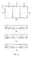
- the first grating region 8 and the second grating region 9 also can be configured as shown in Fig. 2.
- Fig. 2A is a top view of the diffraction grating 2.
- Figs. 2B - D are cross-sectional views in the arrow direction taken along I - I in Fig. 2A. In Figs. 2B - D, the dotted lines indicate that the same shape repeats over and over.
- the depth of the diffraction grating in the first grating region 8 can be different from the depth of the diffraction grating in the second grating region 9. For example, if the depth of the diffraction grating in the first grating region 8 is made smaller than the depth of the diffraction grating in the second grating region 9 as shown in Fig. 2B, then the diffraction efficiency of the zero-order diffraction light in the first grating region 8 is set to be larger than the diffraction efficiency of the zero-order diffraction light in the second grating region 9.
- a stepwise variation of the depth of the diffraction grating with a constant period in the first grating region 8 or the second grating region 9 is also possible.
- the depth of the diffraction gratings in the first grating region 8 varies stepwise, and the depth of the diffraction grating in the first grating region 8 is made smaller than the depth of the diffraction grating in the second grating region 9 as shown in Fig. 2C, then the diffraction efficiency of the zero-order diffraction light in the first grating region 8 is set to be larger than the diffraction efficiency of the zero-order diffraction light in the second grating region 9, which improves the light utilization efficiency.
- the occurrence of -1-order diffraction light can be suppressed. That is to say, the zero-order diffraction efficiency of the grating region 8 is enhanced even further, which not only increases the light utilization efficiency, but also improves the S/N ratio of the reproduction signal and the tracking error signal, because interferences between the main beam and the sub-beams are suppressed.
- the diffraction grating in the first grating region 8 is a blazed grating (saw-tooth-shaped) as shown in Fig. 2D, then the S/N ratio of the reproduction signal and the tracking error signal is improved even further, because the occurrence of -1-order diffraction light can be suppressed completely.
- the diffraction grating pattern of the first grating region 8 also can be different from the diffraction grating pattern of the second grating region 9.
- the first grating region 8 also can be composed of a plurality of regions with diffraction gratings having different grating directions as shown in Fig. 3B.
- the first grating region 8 stripe-shaped, and tilt the direction of the diffraction grating of the second grating region 9 by a predetermined angle against the direction of the diffraction pitch of the first grating region 8.
- the diffraction efficiency of the zero-order diffraction light in the first grating region 8 can be set to be larger than the diffraction efficiency of the zero-order diffraction light in the second grating region 9, and if, for example, a tracking error signal is detected with the three-beam method, then it becomes easy to realize an arrangement wherein the focus spots of the main beam and the sub-beams are separated by a distance of only 1/4 the track pitch on the information recording medium 6.
- the width of the first grating region 8 in the Y-axis direction is at least 2d tan(sin -1 (NA)), wherein d is the distance from the emission plane of the semiconductor laser element 1 to the diffraction grating 2, and NA is the numerical aperture of the collimator lens 4, then only the zero-order diffraction light passing through the first grating region 8 becomes the main beam. Consequently, the intensity of the main beam becomes completely independent of the diffraction efficiency of the second grating region 9, so that the diffraction efficiency of the first grating region 8 can be set freely without giving consideration to the intensity of the sub-beams.
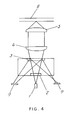
- the diffraction grating 2 and the holographic element 3 are integrated into one component, as shown in Fig. 4, then the number of optical components can be reduced, and the optical device can be made smaller and thinner.
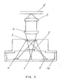
- the semiconductor laser element 1 and the photodetector groups 7 are arranged in the same package 14, and this package 14 is sealed with an optical component, into which the diffraction grating 2 and the holographic element 3 are integrated, as shown in Fig. 5, then the optical system can be made smaller and thinner, while increasing the reliability of the optical device considerably.
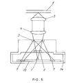
- integrating the semiconductor laser element 1 and the photodetector groups 7 into one component on a silicon substrate 15, as shown in Fig. 6, makes the assembly easier than if separate elements are arranged inside the package 14.
- semiconductor micro-processing technology it is possible to integrate on substrate 15 a circuit for current-voltage conversion and evaluation of the electric signals from the photodetector groups 7. This makes it possible to reduce noise caused by the wiring inside the optical device, so that an optical device with a better S/N ratio can be realized.
- This integration can be realized as a hybrid structure by bonding the chip to the semiconductor laser element 1, after forming all the photodetector groups 7 by semiconductor micro-processing technology on a silicon substrate 15.
- the semiconductor laser element 1 is of the surface-emitting type, the emitting surface should be faced upward and chip-bonded. If the semiconductor laser element 1 is of the end face-emitting type, it is possible to form a concave portion in the substrate 15 by semiconductor micro-processing technology, as shown in Fig. 7, and to chip-bond the semiconductor laser element 1 into this portion.
- a micro-mirror 17 is formed by forming a face slant at an angle of 45° in this concave portion, and depositing a metal or a dielectric film on this face, then the light emitted from the semiconductor laser element 1 is reflected from the micro-mirror 17, so that the light can be guided in an upward direction.
- a monitoring photodetector 16 for receiving the light emitted by the semiconductor laser element 1 from the side that is opposite to the micro-mirror 17, and adjusting the output of the semiconductor laser element 1.
- This configuration has the effect that the optical output of the semiconductor laser element 1 can be adjusted constantly to the optimal output, and waste of electric power due to excessive optical output can be avoided.
- semiconductor hetero-epitaxy it is also possible to use semiconductor hetero-epitaxy to form a compound semiconductor layer (not shown in the drawings) monolithically on the silicon substrate 15, and to form the semiconductor laser element 1 and the photodetector groups 7 on the silicon substrate 15 or on the compound semiconductor layer.
- the semiconductor laser element 1 and the photodetector groups 7 can be integrated into one component without using the silicon substrate 15, and using only the compound semiconductor layer.
- the present embodiment has been explained for an optical device in which both the +1-order diffraction light and the -1-order diffraction light of the holographic element 3 are used to detect the reproduction signal and the various servo signals.
- the number of photodetectors constituting the photodetector groups 7 can be reduced, which makes the optical device cheaper.
- a polarization beam splitter 18, a reflector 19, a polarization separator 20 and a photodetector group 21 for polarization signal detection makes optomagnetic signal detection possible.
- the light that is reflected from the information recording medium 6 and incident on the polarization beam splitter 18 is split up into a beam that travels towards the holographic element 3 and a beam that travels towards the reflector 19.
- the reflected light that has been split by the polarization beam splitter 18 and travels towards the holographic element 3 is diffracted and focussed by the holographic element 3 onto the photodetector group 7, and is used to calculate and/or detect the servo signal, as explained above.
- the returning light that is split by the polarization beam splitter 18 and travels toward the reflector 19 is reflected by the reflector 19, polarized and separated into P-polarized light and S-polarized light by the polarization separator 20, and guided to the photodetector group 21 for polarization signal detection, whereupon the reproduction signal is calculated.
- the light utilization efficiency of optical devices for optomagnetic signal detection which are often said to have an inferior light utilization efficiency, can be improved, which enables operation with a semiconductor laser element with low output power.
- a high-quality reproduction signal can be attained.
- the diffraction efficiency of the ⁇ 1-order diffraction light is reduced, because the diffraction efficiency of the zero-order diffraction light of the first grating region 8 is increased. Consequently, since the influence of multiple reflection is suppressed, interference effects between the main beam and the sub-beams can be decreased. Therefore, the synergy of this effect and the effect of increasing the light utilization efficiency enhances the S/N ratio of the reproduction signal and the tracking error signal. For the same reason, an offset of the tracking error signal is also reduced.
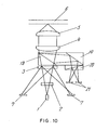
- the polarization beam splitter 18, the reflector 19, and the polarization separator 20 are integrated into one component, as shown in Fig. 10, the number of optical components can be reduced, so that the optical device can be made smaller, thinner and cheaper.
- the semiconductor laser element 1, the photodetector groups 7 and the photodetector group 21 for polarization signal detection are integrated on a substrate 15, arranged in a package 14, and this package 14 is sealed with an optical component, into which the diffraction grating 2 and the holographic element 3 are integrated, and the polarization beam splitter 18, the reflector 19, and the polarization separator 20 are integrated into one component and mounted on the optical component into which the diffraction grating 2 and the holographic element 3 have been integrated, as shown in Fig. 11, then the optical device can be made smaller and thinner, while increasing the reliability of the optical device considerably.
- the configuration of the optical device in the second embodiment is basically the same as that in the first embodiment, but the structure of the diffraction grating 2 in the second embodiment of the present invention differs from the one in the first embodiment in the following aspects.
- Fig. 12 is a top view of the diffraction grating 2 of the optical device in the second embodiment.
- the orientations of the X-axis, the Y-axis and the Z-axis in Fig. 12 are the same as the respective orientations of the X-axis, the Y-axis and the Z-axis in Fig. 13.
- gratings parallel to the X-axis and having a constant pitch are formed for the diffraction grating 2.
- the location of the non-grating region 10 corresponds to the location where the first grating region 8 is formed in the diffraction grating 2 in the first embodiment.
- the zero-order diffraction light passing the first diffraction region 8 in the diffraction grating 2 is used as the main beam, and to increase the intensity of the main beam, it is preferable that the diffraction efficiency of the zero-order diffraction light in the first grating region 8 is set to 100%.
- optical device in the second embodiment can be used for optical information processing systems other than systems for reproduction / recording of an information recording medium.
- the grating of the diffraction grating 2 can be tilted by a predetermined angle with respect to the stripe-shaped non-grating region 10.
- the diffraction grating in the optical device of the present invention which splits the light emitted from a semiconductor laser element into a plurality of beams, with a plurality of diffraction grating regions with different functions
- the light utilization efficiency of the optical device can be increased vastly, so that the light amount of both the main beam and the sub-beams can be increased without increasing the light emission of the semiconductor laser element, and the S/N ratio of the main beam and the sub-beams can be enhanced.
- the ⁇ 1-order diffraction efficiency of the first grating region for transmitting the main beam in the optical device of the present invention lower than the ⁇ 1-order diffraction efficiency of the second grating region, multiple reflections between the information recording medium and the semiconductor laser element can be suppressed, so that the offset of the tracking error signal is reduced.
Landscapes
- Physics & Mathematics (AREA)
- Optics & Photonics (AREA)
- General Physics & Mathematics (AREA)
- Optical Head (AREA)
- Optical Recording Or Reproduction (AREA)
- Semiconductor Lasers (AREA)
- Light Receiving Elements (AREA)
- Diffracting Gratings Or Hologram Optical Elements (AREA)
Claims (5)
- Dispositif optique comprenant:un élément électroluminescent (1) pour irradier de la lumière sur un moyen d'enregistrement d'information (6) ;un réseau de diffraction (2) formée dans un plan X-Y pour diviser la lumière émise depuis ledit élément électroluminescent dans une pluralité de rayons, le réseau de diffraction comprenant une première région de réseau (8 ;10) parallèle à l'axe X et une deuxième région de réseau (9) parallèle à l'axe X avec une efficacité de diffraction qui est différente d'une efficacité de diffraction de la première région de réseau (8 ;10) ;un élément de focalisation (4) pour focaliser les rayons qui ont été divisés par le réseau de diffraction sur le moyen d'enregistrement d'information (6) ;un élément de déviation pour dévier la pluralité de rayons après qui ont été réfléchis depuis le moyen d'enregistrement d'information ; etun photo détecteur (7) pour recevoir la pluralité de rayons après qu'ils ont été déviés par l'élément de déviation ;dans lequel une efficacité de diffraction de lumière de diffraction d'ordre zéro dans la première région de réseau (8 ;10) est plus grande qu'une efficacité de lumière de diffraction d'ordre zéro dans la deuxième région de réseau (9), et
la lumière de diffraction d'ordre zéro provenant de la première région de réseau (8 ;10) est utilisée comme rayon principal pour enregistrer/reproduire un signal d'information sur/depuis le moyen d'enregistrement d'information ;
une lumière de diffraction d'ordre +1 et/ou -1 provenant de la deuxième région de réseau (9) est utilisée comme sous rayon pour détecter un signal d'erreur de piste ; et
le sous rayon entier passe à travers la deuxième région de réseau (9), dans lequel :la première région de réseau est en forme de piste (8) ; etle réseau dans la première région de réseau (8) et le réseau dans la deuxième région de réseau (9) sont parallèles. - Dispositif optique selon la revendication 1, dans lequel une profondeur de réseau de diffraction dans la première région de réseau (8 ; 10) est différente d'une profondeur de réseau de diffraction dans la deuxième région de réseau (9).
- Dispositif optique selon la revendication 1, dans lequel une profondeur de réseau de diffraction dans la première région de réseau (8 ; 10) et/ou une profondeur de réseau de diffraction dans la deuxième région de réseau (9) change pas à pas avec une période constante.
- Dispositif optique selon la revendication 1, dans lequel un réseau de diffraction dans la première région de réseau (8 ; 10) et/ou un réseau de diffraction dans la deuxième région de réseau (9) est un réseau blazé.
- Dispositif optique selon la revendication 1, dans lequel le motif de réseau de diffraction dans la première région de réseau (8 ; 10) est différent du motif de réseau de diffraction dans la deuxième région de réseau (9).
Priority Applications (1)
| Application Number | Priority Date | Filing Date | Title |
|---|---|---|---|
| EP06014544A EP1708186A3 (fr) | 1999-04-28 | 2000-04-27 | Dispositif optique |
Applications Claiming Priority (4)
| Application Number | Priority Date | Filing Date | Title |
|---|---|---|---|
| JP12270999 | 1999-04-28 | ||
| JP12270999 | 1999-04-28 | ||
| JP2000122877A JP2001014717A (ja) | 1999-04-28 | 2000-04-24 | 光学装置 |
| JP2000122877 | 2000-04-24 |
Related Child Applications (1)
| Application Number | Title | Priority Date | Filing Date |
|---|---|---|---|
| EP06014544A Division EP1708186A3 (fr) | 1999-04-28 | 2000-04-27 | Dispositif optique |
Publications (3)
| Publication Number | Publication Date |
|---|---|
| EP1049085A2 EP1049085A2 (fr) | 2000-11-02 |
| EP1049085A3 EP1049085A3 (fr) | 2000-12-06 |
| EP1049085B1 true EP1049085B1 (fr) | 2007-08-22 |
Family
ID=26459785
Family Applications (2)
| Application Number | Title | Priority Date | Filing Date |
|---|---|---|---|
| EP06014544A Withdrawn EP1708186A3 (fr) | 1999-04-28 | 2000-04-27 | Dispositif optique |
| EP00303529A Expired - Lifetime EP1049085B1 (fr) | 1999-04-28 | 2000-04-27 | Dispositif optique |
Family Applications Before (1)
| Application Number | Title | Priority Date | Filing Date |
|---|---|---|---|
| EP06014544A Withdrawn EP1708186A3 (fr) | 1999-04-28 | 2000-04-27 | Dispositif optique |
Country Status (6)
| Country | Link |
|---|---|
| US (3) | US6501601B1 (fr) |
| EP (2) | EP1708186A3 (fr) |
| JP (1) | JP2001014717A (fr) |
| CN (1) | CN1203478C (fr) |
| DE (1) | DE60036049T2 (fr) |
| SG (1) | SG85174A1 (fr) |
Families Citing this family (33)
| Publication number | Priority date | Publication date | Assignee | Title |
|---|---|---|---|---|
| GB0010859D0 (en) * | 2000-05-05 | 2000-06-28 | Green B J | Method of information emission and apparatus therefor |
| JP2002116314A (ja) * | 2000-10-06 | 2002-04-19 | Sankyo Seiki Mfg Co Ltd | 回折素子および光ピックアップ装置 |
| US6692830B2 (en) * | 2001-07-31 | 2004-02-17 | Flex Products, Inc. | Diffractive pigment flakes and compositions |
| JP2003199019A (ja) * | 2001-12-26 | 2003-07-11 | Sony Corp | 撮像装置および方法、記録媒体、並びにプログラム |
| US7136344B2 (en) * | 2003-04-25 | 2006-11-14 | Nec Corporation | Optical head device and optical information recording/reproducing apparatus |
| DE10322238B4 (de) * | 2003-05-17 | 2007-10-31 | Carl Zeiss Smt Ag | Diffraktives optisches Element sowie Projektionsobjektiv mit einem solchen Element |
| JP4245995B2 (ja) * | 2003-07-02 | 2009-04-02 | 株式会社リコー | 光ピックアップ及びこれを用いる光情報処理装置 |
| JP4015116B2 (ja) | 2004-01-08 | 2007-11-28 | シャープ株式会社 | 光集積ユニット、光ピックアップ装置および光ディスク装置 |
| KR100906475B1 (ko) * | 2004-01-13 | 2009-07-08 | 삼성전자주식회사 | 마이크로 광학벤치 구조물 및 그 제조방법 |
| JP2005322849A (ja) * | 2004-05-11 | 2005-11-17 | Nec Compound Semiconductor Devices Ltd | 半導体レーザおよびその製造方法 |
| JP3836483B2 (ja) * | 2004-08-25 | 2006-10-25 | シャープ株式会社 | 光集積ユニットおよびそれを備えた光ピックアップ装置 |
| US20060066948A1 (en) * | 2004-09-24 | 2006-03-30 | Matsushita Electric Industrial Co., Ltd. | Multi-level and gray-level diffraction gratings |
| US20060082838A1 (en) * | 2004-10-18 | 2006-04-20 | Ming-Der Chou | Carriage used in image scanning devices |
| CN101061538A (zh) * | 2004-11-16 | 2007-10-24 | 松下电器产业株式会社 | 光拾取装置 |
| US7593306B2 (en) * | 2004-11-18 | 2009-09-22 | Samsung Electronics Co., Ltd. | Diffraction element and optical pick-up apparatus having the same |
| KR100692574B1 (ko) | 2005-05-11 | 2007-03-13 | 삼성전자주식회사 | 회절소자 및 이를 포함하는 광픽업장치 |
| KR100754517B1 (ko) * | 2005-01-20 | 2007-09-03 | 삼성전자주식회사 | 회절소자 및 이를 포함하는 광픽업장치 |
| KR100659293B1 (ko) * | 2005-01-20 | 2006-12-20 | 삼성전자주식회사 | 회절소자 및 이를 포함하는 광픽업장치 |
| US20080310283A1 (en) * | 2005-07-13 | 2008-12-18 | Arima Devices Corporation | Method of Reading Out Information from a Multiple Layer Optical Recording Medium and Optical Readout Device |
| JP4180073B2 (ja) * | 2005-07-28 | 2008-11-12 | シャープ株式会社 | 光ピックアップ装置 |
| AU2006249295A1 (en) | 2005-12-15 | 2007-07-05 | Jds Uniphase Corporation | Security device with metameric features using diffractive pigment flakes |
| JP2007172793A (ja) * | 2005-12-26 | 2007-07-05 | Sony Corp | 光ピックアップ装置および光ディスク装置 |
| JP4729418B2 (ja) * | 2006-03-03 | 2011-07-20 | 株式会社日立メディアエレクトロニクス | 回折格子、光ピックアップ装置、光ディスク装置 |
| JP2007273015A (ja) * | 2006-03-31 | 2007-10-18 | Matsushita Electric Ind Co Ltd | 光ピックアップ装置 |
| US20070258344A1 (en) * | 2006-05-04 | 2007-11-08 | Imation Corp. | Simultaneously accessing multiple layers of optical disks |
| JPWO2008026506A1 (ja) * | 2006-08-28 | 2010-01-21 | パナソニック株式会社 | 光学ヘッドおよび光ディスク装置 |
| KR101450934B1 (ko) * | 2007-04-06 | 2014-10-14 | 아사히 가라스 가부시키가이샤 | 광헤드 장치 |
| US8922783B2 (en) * | 2007-04-27 | 2014-12-30 | Bodkin Design And Engineering Llc | Multiband spatial heterodyne spectrometer and associated methods |
| JP4951538B2 (ja) | 2008-01-21 | 2012-06-13 | 株式会社日立メディアエレクトロニクス | 光ピックアップ装置および光ディスク装置 |
| US8279525B2 (en) * | 2008-05-21 | 2012-10-02 | Lumella, Inc. | Three-dimensional diffractive structure, method for making, and applications thereof |
| KR102444288B1 (ko) | 2017-11-08 | 2022-09-16 | 삼성전자주식회사 | 메타 렌즈를 포함하는 프로젝터 |
| CN110098559A (zh) * | 2018-01-29 | 2019-08-06 | 山东华光光电子股份有限公司 | 一种半导体激光器壳内准直的装置及方法 |
| CN114335207B (zh) * | 2021-12-31 | 2023-11-24 | 中山大学 | 一种基于双层亚波长光栅的锗硅光电探测器 |
Family Cites Families (34)
| Publication number | Priority date | Publication date | Assignee | Title |
|---|---|---|---|---|
| JPS63138625A (ja) | 1986-11-29 | 1988-06-10 | Toshiba Corp | 電子管 |
| JPS6453359A (en) | 1987-08-24 | 1989-03-01 | Sharp Kk | Optical pickup device |
| DE3855936T2 (de) | 1987-08-24 | 1998-01-02 | Sharp Kk | Optische Abtastvorrichtung |
| JPH0770065B2 (ja) * | 1988-04-20 | 1995-07-31 | シャープ株式会社 | 光ピックアップ装置 |
| JP2865223B2 (ja) * | 1990-12-28 | 1999-03-08 | 松下電子工業株式会社 | 光ピックアップ用偏光板および光ピックアップ装置 |
| TW213519B (fr) | 1991-08-01 | 1993-09-21 | Philips Nv | |
| US5353267A (en) | 1992-06-02 | 1994-10-04 | Nec Corporation | Magneto-optical light detector apparatus |
| US5815293A (en) | 1993-02-01 | 1998-09-29 | Matsushita Electric Industrial Co., Ltd. | Compound objective lens having two focal points |
| EP0612068B1 (fr) | 1993-02-16 | 2000-05-03 | Nec Corporation | Tête optique ainsi que polariseur à réseau de diffraction biréfringent et hologramme polarisant utilisés. |
| JP2658818B2 (ja) | 1993-02-24 | 1997-09-30 | 日本電気株式会社 | 複屈折回折格子型偏光子及び光ヘッド装置 |
| JP3108976B2 (ja) | 1993-03-26 | 2000-11-13 | 松下電子工業株式会社 | 光ヘッドのトラッキング誤差検出装置 |
| US5517479A (en) | 1993-03-26 | 1996-05-14 | Matsushita Electronics Corporation | Optical head including a semiconductor laser having a non-scatter incident area |
| JPH06325400A (ja) | 1993-05-11 | 1994-11-25 | Canon Inc | 光学式情報記録再生装置 |
| JP3172360B2 (ja) | 1994-05-09 | 2001-06-04 | 三洋電機株式会社 | ビーム3分割用反射型回折格子およびこれを用いた光ピックアップ |
| JPH08124204A (ja) | 1994-10-24 | 1996-05-17 | Sanyo Electric Co Ltd | 光ピックアップ装置 |
| KR100373801B1 (ko) | 1994-07-29 | 2003-05-09 | 산요 덴키 가부시키가이샤 | 반도체레이저장치및이를이용한광픽업장치 |
| JP3660415B2 (ja) | 1995-02-07 | 2005-06-15 | 富士通株式会社 | 光学記憶装置用光学デバイス |
| JPH08339568A (ja) | 1995-06-12 | 1996-12-24 | Canon Inc | 光学的情報記録再生装置 |
| US5835471A (en) | 1995-06-12 | 1998-11-10 | Canon Kabushiki Kaisha | Optical information recording and/or reproducing apparatus |
| JPH0980211A (ja) | 1995-09-12 | 1997-03-28 | Matsushita Electric Ind Co Ltd | 一体光学素子とその製造方法 |
| JP3493855B2 (ja) | 1995-12-14 | 2004-02-03 | 旭硝子株式会社 | 光ヘッド装置の製造方法及び製造装置 |
| US5652744A (en) | 1996-02-08 | 1997-07-29 | Industrial Technology Research Institute | Single surface diffractive element for optical pickup heads |
| JP3732268B2 (ja) | 1996-02-28 | 2006-01-05 | 富士通株式会社 | 光ディスク装置用光学ヘッド |
| JPH09306054A (ja) | 1996-05-20 | 1997-11-28 | Hitachi Ltd | 光磁気ディスク装置 |
| US5662744A (en) * | 1996-06-05 | 1997-09-02 | Maytag Corporation | Wash arm for dishwasher |
| JP3301765B2 (ja) | 1996-10-31 | 2002-07-15 | 三洋電機株式会社 | 光ピックアップ装置 |
| TW350571U (en) | 1996-11-23 | 1999-01-11 | Ind Tech Res Inst | Optical grille form of optical read head in digital CD-ROM player |
| JPH10255309A (ja) | 1997-03-07 | 1998-09-25 | Sanyo Electric Co Ltd | 光ピックアップ装置 |
| JP3658928B2 (ja) | 1997-07-09 | 2005-06-15 | 旭硝子株式会社 | 光ヘッド装置 |
| JPH11110781A (ja) | 1997-10-01 | 1999-04-23 | Matsushita Electron Corp | 半導体レーザ装置 |
| CN1130708C (zh) | 1997-10-01 | 2003-12-10 | 松下电器产业株式会社 | 半导体激光装置 |
| JPH11110782A (ja) | 1997-10-01 | 1999-04-23 | Matsushita Electron Corp | 半導体レーザ装置 |
| JPH11167012A (ja) * | 1997-12-03 | 1999-06-22 | Fuji Photo Optical Co Ltd | 回折型フィルタ |
| JP2000011424A (ja) | 1998-06-24 | 2000-01-14 | Asahi Glass Co Ltd | 光ヘッド装置 |
-
2000
- 2000-04-24 JP JP2000122877A patent/JP2001014717A/ja active Pending
- 2000-04-25 US US09/557,711 patent/US6501601B1/en not_active Expired - Fee Related
- 2000-04-26 SG SG200002289A patent/SG85174A1/en unknown
- 2000-04-27 EP EP06014544A patent/EP1708186A3/fr not_active Withdrawn
- 2000-04-27 DE DE60036049T patent/DE60036049T2/de not_active Expired - Fee Related
- 2000-04-27 EP EP00303529A patent/EP1049085B1/fr not_active Expired - Lifetime
- 2000-04-28 CN CN00107084.3A patent/CN1203478C/zh not_active Expired - Fee Related
-
2002
- 2002-09-20 US US10/251,471 patent/US6728035B2/en not_active Expired - Fee Related
- 2002-11-04 US US10/287,953 patent/US20030053211A1/en not_active Abandoned
Also Published As
| Publication number | Publication date |
|---|---|
| US20030016448A1 (en) | 2003-01-23 |
| EP1049085A3 (fr) | 2000-12-06 |
| CN1271933A (zh) | 2000-11-01 |
| DE60036049D1 (de) | 2007-10-04 |
| US6728035B2 (en) | 2004-04-27 |
| DE60036049T2 (de) | 2007-12-06 |
| CN1203478C (zh) | 2005-05-25 |
| SG85174A1 (en) | 2001-12-19 |
| EP1049085A2 (fr) | 2000-11-02 |
| US6501601B1 (en) | 2002-12-31 |
| EP1708186A2 (fr) | 2006-10-04 |
| EP1708186A3 (fr) | 2006-10-18 |
| US20030053211A1 (en) | 2003-03-20 |
| JP2001014717A (ja) | 2001-01-19 |
Similar Documents
| Publication | Publication Date | Title |
|---|---|---|
| EP1049085B1 (fr) | Dispositif optique | |
| JP2710675B2 (ja) | 光学情報記録再生用光ヘッド | |
| US7139235B2 (en) | Optical element with diffraction grating, semiconductor device, and optical information recording device employing the same | |
| KR100479701B1 (ko) | 광전자 장치 | |
| EP0556062B1 (fr) | Unité de source de lumière et tête optique équipée de telle unité | |
| EP0188624B1 (fr) | Dispositif de detection d'erreurs de suivi de piste d'une tete optique | |
| JPH05298721A (ja) | 光ヘッド | |
| US7843794B2 (en) | Optical pickup and optical disk apparatus | |
| KR100481735B1 (ko) | 집적 광학 부재 및 광 픽업 장치 | |
| EP0543481B1 (fr) | Appareil de reproduction d'information avec des assemblages de photodétecteurs localisés séparément | |
| JP3108976B2 (ja) | 光ヘッドのトラッキング誤差検出装置 | |
| JP2004047093A (ja) | 光学装置 | |
| KR20060048871A (ko) | 반도체레이저장치 및 광 픽업장치 | |
| JPH07161065A (ja) | 光ピックアップ装置 | |
| JPH02162541A (ja) | 光学式信号再生装置及びそれに用いる光学部品 | |
| JP3163184B2 (ja) | 半導体レーザ装置 | |
| JPH11110781A (ja) | 半導体レーザ装置 | |
| JP2005128211A (ja) | 光学素子およびそれを用いた光学装置 | |
| JPH07192299A (ja) | 光ピックアップ装置 | |
| JPH05120754A (ja) | 光ピツクアツプ | |
| JP2001184694A (ja) | 光ピックアップ装置および光源ユニット | |
| KR100417022B1 (ko) | 복합광학부품 및 이를 이용한 광픽업 | |
| JPH04248134A (ja) | 光ピックアップ | |
| JPH08321066A (ja) | 光ピックアップ | |
| JP2000021012A (ja) | 光ピックアップ装置 |
Legal Events
| Date | Code | Title | Description |
|---|---|---|---|
| PUAI | Public reference made under article 153(3) epc to a published international application that has entered the european phase |
Free format text: ORIGINAL CODE: 0009012 |
|
| PUAL | Search report despatched |
Free format text: ORIGINAL CODE: 0009013 |
|
| AK | Designated contracting states |
Kind code of ref document: A2 Designated state(s): DE FR GB NL |
|
| AX | Request for extension of the european patent |
Free format text: AL;LT;LV;MK;RO;SI |
|
| AK | Designated contracting states |
Kind code of ref document: A3 Designated state(s): AT BE CH CY DE DK ES FI FR GB GR IE IT LI LU MC NL PT SE |
|
| AX | Request for extension of the european patent |
Free format text: AL;LT;LV;MK;RO;SI |
|
| 17P | Request for examination filed |
Effective date: 20010126 |
|
| RAP1 | Party data changed (applicant data changed or rights of an application transferred) |
Owner name: MATSUSHITA ELECTRIC INDUSTRIAL CO., LTD. |
|
| AKX | Designation fees paid |
Free format text: DE FR GB NL |
|
| 17Q | First examination report despatched |
Effective date: 20060224 |
|
| GRAP | Despatch of communication of intention to grant a patent |
Free format text: ORIGINAL CODE: EPIDOSNIGR1 |
|
| GRAS | Grant fee paid |
Free format text: ORIGINAL CODE: EPIDOSNIGR3 |
|
| GRAA | (expected) grant |
Free format text: ORIGINAL CODE: 0009210 |
|
| AK | Designated contracting states |
Kind code of ref document: B1 Designated state(s): DE FR GB NL |
|
| REG | Reference to a national code |
Ref country code: GB Ref legal event code: FG4D |
|
| REF | Corresponds to: |
Ref document number: 60036049 Country of ref document: DE Date of ref document: 20071004 Kind code of ref document: P |
|
| ET | Fr: translation filed | ||
| PLBE | No opposition filed within time limit |
Free format text: ORIGINAL CODE: 0009261 |
|
| STAA | Information on the status of an ep patent application or granted ep patent |
Free format text: STATUS: NO OPPOSITION FILED WITHIN TIME LIMIT |
|
| 26N | No opposition filed |
Effective date: 20080526 |
|
| PGFP | Annual fee paid to national office [announced via postgrant information from national office to epo] |
Ref country code: NL Payment date: 20090427 Year of fee payment: 10 Ref country code: FR Payment date: 20090417 Year of fee payment: 10 Ref country code: DE Payment date: 20090428 Year of fee payment: 10 |
|
| PGFP | Annual fee paid to national office [announced via postgrant information from national office to epo] |
Ref country code: GB Payment date: 20090422 Year of fee payment: 10 |
|
| REG | Reference to a national code |
Ref country code: NL Ref legal event code: V1 Effective date: 20101101 |
|
| GBPC | Gb: european patent ceased through non-payment of renewal fee |
Effective date: 20100427 |
|
| REG | Reference to a national code |
Ref country code: FR Ref legal event code: ST Effective date: 20101230 |
|
| PG25 | Lapsed in a contracting state [announced via postgrant information from national office to epo] |
Ref country code: NL Free format text: LAPSE BECAUSE OF NON-PAYMENT OF DUE FEES Effective date: 20101101 |
|
| PG25 | Lapsed in a contracting state [announced via postgrant information from national office to epo] |
Ref country code: DE Free format text: LAPSE BECAUSE OF NON-PAYMENT OF DUE FEES Effective date: 20101103 |
|
| PG25 | Lapsed in a contracting state [announced via postgrant information from national office to epo] |
Ref country code: GB Free format text: LAPSE BECAUSE OF NON-PAYMENT OF DUE FEES Effective date: 20100427 |
|
| PG25 | Lapsed in a contracting state [announced via postgrant information from national office to epo] |
Ref country code: FR Free format text: LAPSE BECAUSE OF NON-PAYMENT OF DUE FEES Effective date: 20100430 |