EP1049155A1 - Herstellungsverfahren für eine SOI Scheibe mit vergrabenen Oxidbereichen ohne Spitzen - Google Patents
Herstellungsverfahren für eine SOI Scheibe mit vergrabenen Oxidbereichen ohne Spitzen Download PDFInfo
- Publication number
- EP1049155A1 EP1049155A1 EP99830256A EP99830256A EP1049155A1 EP 1049155 A1 EP1049155 A1 EP 1049155A1 EP 99830256 A EP99830256 A EP 99830256A EP 99830256 A EP99830256 A EP 99830256A EP 1049155 A1 EP1049155 A1 EP 1049155A1
- Authority
- EP
- European Patent Office
- Prior art keywords
- regions
- trenches
- forming
- process according
- wafer
- Prior art date
- Legal status (The legal status is an assumption and is not a legal conclusion. Google has not performed a legal analysis and makes no representation as to the accuracy of the status listed.)
- Withdrawn
Links
Images




Classifications
-
- H—ELECTRICITY
- H10—SEMICONDUCTOR DEVICES; ELECTRIC SOLID-STATE DEVICES NOT OTHERWISE PROVIDED FOR
- H10P—GENERIC PROCESSES OR APPARATUS FOR THE MANUFACTURE OR TREATMENT OF DEVICES COVERED BY CLASS H10
- H10P14/00—Formation of materials, e.g. in the shape of layers or pillars
- H10P14/60—Formation of materials, e.g. in the shape of layers or pillars of insulating materials
- H10P14/63—Formation of materials, e.g. in the shape of layers or pillars of insulating materials characterised by the formation processes
- H10P14/6302—Non-deposition formation processes
- H10P14/6304—Formation by oxidation, e.g. oxidation of the substrate
- H10P14/6306—Formation by oxidation, e.g. oxidation of the substrate of the semiconductor materials
- H10P14/6308—Formation by oxidation, e.g. oxidation of the substrate of the semiconductor materials of Group IV semiconductors
- H10P14/6309—Formation by oxidation, e.g. oxidation of the substrate of the semiconductor materials of Group IV semiconductors of silicon in uncombined form, i.e. pure silicon
-
- H—ELECTRICITY
- H10—SEMICONDUCTOR DEVICES; ELECTRIC SOLID-STATE DEVICES NOT OTHERWISE PROVIDED FOR
- H10P—GENERIC PROCESSES OR APPARATUS FOR THE MANUFACTURE OR TREATMENT OF DEVICES COVERED BY CLASS H10
- H10P14/00—Formation of materials, e.g. in the shape of layers or pillars
- H10P14/60—Formation of materials, e.g. in the shape of layers or pillars of insulating materials
- H10P14/61—Formation of materials, e.g. in the shape of layers or pillars of insulating materials using masks
-
- H—ELECTRICITY
- H10—SEMICONDUCTOR DEVICES; ELECTRIC SOLID-STATE DEVICES NOT OTHERWISE PROVIDED FOR
- H10P—GENERIC PROCESSES OR APPARATUS FOR THE MANUFACTURE OR TREATMENT OF DEVICES COVERED BY CLASS H10
- H10P14/00—Formation of materials, e.g. in the shape of layers or pillars
- H10P14/60—Formation of materials, e.g. in the shape of layers or pillars of insulating materials
- H10P14/65—Formation of materials, e.g. in the shape of layers or pillars of insulating materials characterised by treatments performed before or after the formation of the materials
- H10P14/6502—Formation of materials, e.g. in the shape of layers or pillars of insulating materials characterised by treatments performed before or after the formation of the materials of treatments performed before formation of the materials
-
- H—ELECTRICITY
- H10—SEMICONDUCTOR DEVICES; ELECTRIC SOLID-STATE DEVICES NOT OTHERWISE PROVIDED FOR
- H10P—GENERIC PROCESSES OR APPARATUS FOR THE MANUFACTURE OR TREATMENT OF DEVICES COVERED BY CLASS H10
- H10P90/00—Preparation of wafers not covered by a single main group of this subclass, e.g. wafer reinforcement
- H10P90/19—Preparing inhomogeneous wafers
- H10P90/1904—Preparing vertically inhomogeneous wafers
- H10P90/1906—Preparing SOI wafers
- H10P90/1912—Preparing SOI wafers using selective deposition, e.g. epitaxial lateral overgrowth [ELO] or selective deposition of single crystal silicon
-
- H—ELECTRICITY
- H10—SEMICONDUCTOR DEVICES; ELECTRIC SOLID-STATE DEVICES NOT OTHERWISE PROVIDED FOR
- H10W—GENERIC PACKAGES, INTERCONNECTIONS, CONNECTORS OR OTHER CONSTRUCTIONAL DETAILS OF DEVICES COVERED BY CLASS H10
- H10W10/00—Isolation regions in semiconductor bodies between components of integrated devices
- H10W10/01—Manufacture or treatment
- H10W10/011—Manufacture or treatment of isolation regions comprising dielectric materials
- H10W10/012—Manufacture or treatment of isolation regions comprising dielectric materials using local oxidation of silicon [LOCOS]
- H10W10/0121—Manufacture or treatment of isolation regions comprising dielectric materials using local oxidation of silicon [LOCOS] in regions recessed from the surface, e.g. in trenches or grooves
- H10W10/0123—Manufacture or treatment of isolation regions comprising dielectric materials using local oxidation of silicon [LOCOS] in regions recessed from the surface, e.g. in trenches or grooves using auxiliary pillars in the regions
-
- H—ELECTRICITY
- H10—SEMICONDUCTOR DEVICES; ELECTRIC SOLID-STATE DEVICES NOT OTHERWISE PROVIDED FOR
- H10W—GENERIC PACKAGES, INTERCONNECTIONS, CONNECTORS OR OTHER CONSTRUCTIONAL DETAILS OF DEVICES COVERED BY CLASS H10
- H10W10/00—Isolation regions in semiconductor bodies between components of integrated devices
- H10W10/10—Isolation regions comprising dielectric materials
- H10W10/13—Isolation regions comprising dielectric materials formed using local oxidation of silicon [LOCOS], e.g. sealed interface localised oxidation [SILO] or side-wall mask isolation [SWAMI]
-
- H—ELECTRICITY
- H10—SEMICONDUCTOR DEVICES; ELECTRIC SOLID-STATE DEVICES NOT OTHERWISE PROVIDED FOR
- H10W—GENERIC PACKAGES, INTERCONNECTIONS, CONNECTORS OR OTHER CONSTRUCTIONAL DETAILS OF DEVICES COVERED BY CLASS H10
- H10W10/00—Isolation regions in semiconductor bodies between components of integrated devices
- H10W10/10—Isolation regions comprising dielectric materials
- H10W10/181—Semiconductor-on-insulator [SOI] isolation regions, e.g. buried oxide regions of SOI wafers
Definitions
- the present invention regards an improved process for manufacturing a SOI wafer with buried oxide regions without cusps.
- SOI Silicon-on-Insulator
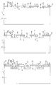
- a process for manufacturing SOI wafers is the subject of European Patent Application No. 98830007.5 filed on 13.1.98 in the name of the present applicant and is described hereinafter with reference to Figures 1 to 8.
- a first silicon oxide layer is initially grown and has a thickness comprised between, for example, 20 and 60 nm. Then a first silicon nitride layer with a thickness comprised between 90 and 150 nm is deposited.
- the resist mask is then removed to obtain the intermediate structure of Figure 1, where the wafer thus obtained is indicated, as a whole, by 1, and the portions of the first oxide layer and of the first nitride layer remaining after dry etching are indicated by 4 and 5, and define respective first protective regions 7 covering first portions 8' of the substrate 2.
- the first protective regions 7 form a hard mask, indicated as a whole by 9, used for etching the substrate 2 at second portions 8" left uncovered by the mask 9 so as to form initial trenches 10 ( Figure 2) .
- the wafer 1 is oxidized, thus forming a second oxide layer 11, having a thickness comprised between, for example, 20 and 60 nm, covering the walls and the bottom of the initial trenches 10, and then a second silicon nitride layer 12 is deposited for a thickness comprised between 90 and 150 nm.
- the layers 12 and 11 are etched anisotropically in an unmasked way. Given the etching anisotropy, the horizontal portions of the second silicon nitride layer 12 and of the silicon oxide layer 11 on the bottom of the initial trenches 10, as well as the portion of the second silicon nitride layer 12 on top of the portions 4 and 5 are removed to yield the intermediate structure of Figure 4, wherein the regions 8' are still covered on top by the mask 9 and laterally (on the vertical walls of the initial trenches 10) by oxide and nitride portions 11' and 12'. Instead, the substrate 2 is bare on the bottom 15 of the initial trenches 10.
- the uncovered silicon at the bottom 15 of the initial trenches 10 are etched to deepen the initial trenches 10 until final trenches 16 are obtained having a desired depth.
- the depth of the final trenches 16 determines the dimensions of the desired buried oxide layer, and hence the electrical characteristics of the SOI wafer, as clarified hereinafter, and is then determined according to the requirements for the final SOI wafer.
- the substrate 2 is now formed by a base portion indicated by 2' and by a number of "columns" 18 extending vertically from the base portion 2'.
- the intermediate structure of Figure 5 is thus obtained, wherein the nitride portions 5 and 12' are no longer distinct from each another and are indicated by 19; also the oxide portions 4 and 11' are no longer distinct from each another and are indicated by 20, and form, together with the portions 19, second protective regions 30.
- a thermal oxidation is then carried out, so that the exposed silicon regions of the "columns" 18 are converted into silicon oxide.
- a gradual growth of the oxide regions is obtained at the expense of the silicon regions, starting from the side walls of the final trenches 16 towards the inside of the columns, and in part also towards and inside the base portion 2'. Since during oxidation the volume increases, the oxide regions being formed occupy, gradually, the space of the final trenches 16 until they completely close the trenches and join together.
- the second protective regions 30 are removed so as to uncover the "tips" 21, which form the nucleus for subsequent epitaxial growth.
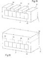
- FIG. 7 which shows the three-dimensional structure of the wafer 1 in this step, is obtained.
- epitaxial growth is performed, the parameters of which are chosen so as to prevent nucleation of the silicon in the areas overlying the buried oxide region 22, and a high side growth/vertical growth ratio is chosen so as to obtain first a horizontal growth of the silicon around the tips 21 (and hence the coating of the top surface of the buried oxide region 22), and subsequently the vertical growth of an epitaxial layer 23.
- the final structure of wafer 1 shown in Figure 8 is thus obtained.
- the shape of the buried oxide region 22 is not ideal.
- the exposed silicon regions of the "columns" 18 are oxidized following the curved lines, so that the buried oxide region 22 presents, at the bottom, a shape defined by a series of arches 35 and, at the top, a shape defined by a series of cusps 37 extending upwards at each wall of the final trenches 16.
- voids 38 are formed inside the buried oxide region 22. This shape of the buried oxide region 22 thus renders the step of epitaxial growth of the silicon to form the SOI wafer critical, and, in any case, the shape of the bottom surface of the epitaxial layer 23 creates problems in forming suspended masses.
- the aim of the present invention is therefore to overcome the drawbacks of the above described manufacturing process.
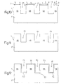
- a "hard” mask is formed, indicated as a whole by 9 and comprising protective regions 7; using the hard mask 9, the uncovered portions of the substrate 2 are etched so as to form trenches 45 separated from each other by protruding regions or "columns" 48 of monocrystalline silicon extending vertically from the base portion 2' (Fig. 10).
- the trenches have a depth comprised between 1 and 3 ⁇ m and a width comprised between 0.3 and 2 ⁇ m.
- a protective layer 50 of silicon oxide having a thickness comprised between 10 and 20 nm is formed (for example, thermally grown) so that the surface of the silicon is not damaged in subsequent manufacturing steps.
- the angle-implant step comprises two subsequent implants, of which a first implant (arrows 61a) is made by inclining the silicon wafer at an angle ⁇ comprised between 7° and 60°, which causes ions to be implanted at the same angle ⁇ with respect to the vertical, and a second implant (arrows 61b) is made symmetrically with respect to the first implant (i.e., with an angle of - ⁇ ).
- the columns 48 partially shield the implant on the walls of the adjacent columns 48.
- first masking regions 55 are formed on the tips of the columns 48 and have a first concentration, in that they receive both the angled implants, and second masking regions 56 are formed on the top part of the walls of the trenches 45 and have a lower concentration.
- the bottom part of the walls and the bottom of the trenches 45 are not, instead, implanted.
- nitrogen is then implanted, keeping the wafer 1 horizontal (implant perpendicular to the surface 3 of the wafer 1).
- This implant reaches the bottom of the trenches 45 and forms retarding regions 57; in addition, it increases the concentration of nitrogen ions in the first masking regions 55 on the tips of the columns 48.
- This implant is performed at a lower dose than the angle-implant; for example, the implant dose D i is here 10 16 -10 17 at/cm 2 with an energy of about 20-30 keV.
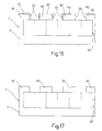
- the wafer 1 has first and second masking regions 55 and 56, at high doses, on the tips of the columns 48 and on the top part of the walls of the trenches 45; retarding regions 57, at low doses, on the bottom of the trenches 45; and surface portions 58, not implanted, on the bottom part of the walls of the trenches 45, where the monocrystalline silicon of the columns 48 is bare.
- an annealing step is carried out for 1-16 hours at a temperature of approximately 1000°C.
- an oxidation step is carried out, during which silicon portions are converted gradually into silicon oxide.
- oxide regions grow horizontally, at the expense of the silicon regions, towards the inside of the columns 48 starting from the surface portions 58 of the side walls of the trenches 45, while the retarding regions 57 temporarily protect the base portion 2'. Because of the far from high concentration of nitrogen in the retarding regions 57, these form, however, only a temporary barrier, and hence, after a first phase, the thermal oxidation proceeds also downwards into the base portion 2'.
- the masking regions 55 and 56 continue, instead, to protect the tips 60 of the columns 48 also in this second step.
- the masking regions 55 and 56 are removed by selective etching using phosphoric acid, so as to uncover the tips 60 of the columns 48 which are to form the nucleus for a subsequent epitaxial growth step.
Landscapes
- Element Separation (AREA)
- Formation Of Insulating Films (AREA)
Priority Applications (3)
| Application Number | Priority Date | Filing Date | Title |
|---|---|---|---|
| EP99830256A EP1049155A1 (de) | 1999-04-29 | 1999-04-29 | Herstellungsverfahren für eine SOI Scheibe mit vergrabenen Oxidbereichen ohne Spitzen |
| US09/558,934 US6362070B1 (en) | 1999-04-29 | 2000-04-26 | Process for manufacturing a SOI wafer with buried oxide regions without cusps |
| JP2000127858A JP2000340775A (ja) | 1999-04-29 | 2000-04-27 | 無尖端埋込酸化膜領域を備えたsoiウエハの製造方法 |
Applications Claiming Priority (1)
| Application Number | Priority Date | Filing Date | Title |
|---|---|---|---|
| EP99830256A EP1049155A1 (de) | 1999-04-29 | 1999-04-29 | Herstellungsverfahren für eine SOI Scheibe mit vergrabenen Oxidbereichen ohne Spitzen |
Publications (1)
| Publication Number | Publication Date |
|---|---|
| EP1049155A1 true EP1049155A1 (de) | 2000-11-02 |
Family
ID=8243382
Family Applications (1)
| Application Number | Title | Priority Date | Filing Date |
|---|---|---|---|
| EP99830256A Withdrawn EP1049155A1 (de) | 1999-04-29 | 1999-04-29 | Herstellungsverfahren für eine SOI Scheibe mit vergrabenen Oxidbereichen ohne Spitzen |
Country Status (3)
| Country | Link |
|---|---|
| US (1) | US6362070B1 (de) |
| EP (1) | EP1049155A1 (de) |
| JP (1) | JP2000340775A (de) |
Cited By (1)
| Publication number | Priority date | Publication date | Assignee | Title |
|---|---|---|---|---|
| DE10240893A1 (de) * | 2002-09-04 | 2004-03-18 | Infineon Technologies Ag | Verfahren zur Herstellung von SONOS-Speicherzellen, SONOS-Speicherzelle und Speicherzellenfeld |
Families Citing this family (11)
| Publication number | Priority date | Publication date | Assignee | Title |
|---|---|---|---|---|
| JP2000058802A (ja) * | 1998-01-13 | 2000-02-25 | Stmicroelectronics Srl | Soiウェハの製造方法 |
| DE10242661A1 (de) * | 2002-09-13 | 2004-03-25 | Conti Temic Microelectronic Gmbh | Verfahren zum Herstellen von Isolationsstrukturen |
| US7190051B2 (en) * | 2003-01-17 | 2007-03-13 | Second Sight Medical Products, Inc. | Chip level hermetic and biocompatible electronics package using SOI wafers |
| US7384857B2 (en) * | 2005-02-25 | 2008-06-10 | Seiko Epson Corporation | Method to fabricate completely isolated silicon regions |
| JP2008536329A (ja) * | 2005-04-14 | 2008-09-04 | エヌエックスピー ビー ヴィ | 半導体デバイスおよびその製造方法 |
| US7777275B2 (en) * | 2006-05-18 | 2010-08-17 | Macronix International Co., Ltd. | Silicon-on-insulator structures |
| KR101057652B1 (ko) * | 2008-11-07 | 2011-08-18 | 주식회사 동부하이텍 | 반도체 소자의 제조 방법 |
| EP2455967B1 (de) * | 2010-11-18 | 2018-05-23 | IMEC vzw | Verfahren zur Bildung einer versenkten dielektrischen Schicht unter einer Halbleiterlamelle |
| US20150069608A1 (en) * | 2013-09-11 | 2015-03-12 | International Business Machines Corporation | Through-silicon via structure and method for improving beol dielectric performance |
| CN110858561A (zh) * | 2018-08-23 | 2020-03-03 | 合肥晶合集成电路有限公司 | 硅岛结构及其制作方法 |
| FR3090615B1 (fr) * | 2018-12-20 | 2020-12-11 | Soitec Silicon On Insulator | Procédé de fabrication d’un dispositif comprenant une membrane surplombant une cavité |
Citations (5)
| Publication number | Priority date | Publication date | Assignee | Title |
|---|---|---|---|---|
| JPS59232437A (ja) * | 1983-06-15 | 1984-12-27 | Matsushita Electric Ind Co Ltd | 半導体装置の製造方法 |
| US4685198A (en) * | 1985-07-25 | 1987-08-11 | Matsushita Electric Industrial Co., Ltd. | Method of manufacturing isolated semiconductor devices |
| US5025302A (en) * | 1981-07-01 | 1991-06-18 | Rockwell International Corporation | PNP type lateral transistor with minimal substrate operation interference |
| EP0488344A2 (de) * | 1990-11-29 | 1992-06-03 | Texas Instruments Incorporated | Herstellung eines SOI Halbleiterkörpers unter Verwendung selektiver epitaxialen Wachsen |
| US5691230A (en) * | 1996-09-04 | 1997-11-25 | Micron Technology, Inc. | Technique for producing small islands of silicon on insulator |
Family Cites Families (6)
| Publication number | Priority date | Publication date | Assignee | Title |
|---|---|---|---|---|
| US4361600A (en) * | 1981-11-12 | 1982-11-30 | General Electric Company | Method of making integrated circuits |
| US4604162A (en) * | 1983-06-13 | 1986-08-05 | Ncr Corporation | Formation and planarization of silicon-on-insulator structures |
| JPS6072243A (ja) * | 1983-09-28 | 1985-04-24 | Matsushita Electric Ind Co Ltd | 半導体集積回路装置 |
| JPH0779133B2 (ja) * | 1986-06-12 | 1995-08-23 | 松下電器産業株式会社 | 半導体装置の製造方法 |
| TW309647B (de) * | 1995-12-30 | 1997-07-01 | Hyundai Electronics Ind | |
| US6238998B1 (en) * | 1998-11-20 | 2001-05-29 | International Business Machines Corporation | Shallow trench isolation on a silicon substrate using nitrogen implant into the side wall |
-
1999
- 1999-04-29 EP EP99830256A patent/EP1049155A1/de not_active Withdrawn
-
2000
- 2000-04-26 US US09/558,934 patent/US6362070B1/en not_active Expired - Fee Related
- 2000-04-27 JP JP2000127858A patent/JP2000340775A/ja active Pending
Patent Citations (5)
| Publication number | Priority date | Publication date | Assignee | Title |
|---|---|---|---|---|
| US5025302A (en) * | 1981-07-01 | 1991-06-18 | Rockwell International Corporation | PNP type lateral transistor with minimal substrate operation interference |
| JPS59232437A (ja) * | 1983-06-15 | 1984-12-27 | Matsushita Electric Ind Co Ltd | 半導体装置の製造方法 |
| US4685198A (en) * | 1985-07-25 | 1987-08-11 | Matsushita Electric Industrial Co., Ltd. | Method of manufacturing isolated semiconductor devices |
| EP0488344A2 (de) * | 1990-11-29 | 1992-06-03 | Texas Instruments Incorporated | Herstellung eines SOI Halbleiterkörpers unter Verwendung selektiver epitaxialen Wachsen |
| US5691230A (en) * | 1996-09-04 | 1997-11-25 | Micron Technology, Inc. | Technique for producing small islands of silicon on insulator |
Non-Patent Citations (1)
| Title |
|---|
| PATENT ABSTRACTS OF JAPAN vol. 009, no. 106 (E - 313) 10 May 1985 (1985-05-10) * |
Cited By (2)
| Publication number | Priority date | Publication date | Assignee | Title |
|---|---|---|---|---|
| DE10240893A1 (de) * | 2002-09-04 | 2004-03-18 | Infineon Technologies Ag | Verfahren zur Herstellung von SONOS-Speicherzellen, SONOS-Speicherzelle und Speicherzellenfeld |
| US7323388B2 (en) | 2002-09-04 | 2008-01-29 | Infineon Technologies Ag | SONOS memory cells and arrays and method of forming the same |
Also Published As
| Publication number | Publication date |
|---|---|
| JP2000340775A (ja) | 2000-12-08 |
| US6362070B1 (en) | 2002-03-26 |
Similar Documents
| Publication | Publication Date | Title |
|---|---|---|
| CA1139017A (en) | Process for making large area isolation trenches | |
| US4929566A (en) | Method of making dielectrically isolated integrated circuits using oxygen implantation and expitaxial growth | |
| EP0107902B1 (de) | Verfahren zur Herstellung von Isolationszonen in Halbleiteranordnungen | |
| EP1073112A1 (de) | Verfahren zur Herstellung eines SOI-Wafers mittels Oxidierung von vergrabenen Hohlräumen | |
| EP0062170B1 (de) | Verfahren zur Herstellung selbstalignierter dielektrischer Isolation | |
| JPH0821613B2 (ja) | Mos装置の分離構造の製造方法 | |
| US6362070B1 (en) | Process for manufacturing a SOI wafer with buried oxide regions without cusps | |
| JPH05206258A (ja) | 半導体構造及びその製造方法 | |
| JPH11204633A (ja) | トレンチ隔離の形成方法 | |
| JP2000315807A (ja) | プレーナ・ヘテロ構造の製造方法 | |
| US6255145B1 (en) | Process for manufacturing patterned silicon-on-insulator layers with self-aligned trenches and resulting product | |
| KR100353174B1 (ko) | 절연체 상 실리콘 기판 제조 방법 | |
| EP1009024B1 (de) | Herstellungsverfahren für eine SOI-Scheibe | |
| JP2000058802A (ja) | Soiウェハの製造方法 | |
| JPH0582441A (ja) | 炭化シリコンバイポーラ半導体装置およびその製造方法 | |
| US6790745B1 (en) | Fabrication of dielectrically isolated regions of silicon in a substrate | |
| JPS6257232A (ja) | アイソレ−シヨンデバイス及びその製法 | |
| EP0929095B1 (de) | Verfahren zur Herstellung eines SOI-Substrates | |
| JPS60208843A (ja) | 半導体装置の製造方法 | |
| JPS6136381B2 (de) | ||
| EP0978872B1 (de) | Ein preiswertes Verfahren zur Herstellung eines SOI-Wafers | |
| JPS5957450A (ja) | 半導体装置の素子分離方法 | |
| JPS63202033A (ja) | 誘電体分離基板の製造方法 | |
| US6593204B2 (en) | Method of fabricating a silicon-on-insulator system with thin semiconductor islets surrounded by an insulative material | |
| EP0948034B1 (de) | Ein Verfahren für die Herstellung einer SO1-Scheibe |
Legal Events
| Date | Code | Title | Description |
|---|---|---|---|
| PUAI | Public reference made under article 153(3) epc to a published international application that has entered the european phase |
Free format text: ORIGINAL CODE: 0009012 |
|
| AK | Designated contracting states |
Kind code of ref document: A1 Designated state(s): DE FR GB IT |
|
| AX | Request for extension of the european patent |
Free format text: AL;LT;LV;MK;RO;SI |
|
| 17P | Request for examination filed |
Effective date: 20010411 |
|
| AKX | Designation fees paid |
Free format text: DE FR GB IT |
|
| 17Q | First examination report despatched |
Effective date: 20061215 |
|
| STAA | Information on the status of an ep patent application or granted ep patent |
Free format text: STATUS: THE APPLICATION IS DEEMED TO BE WITHDRAWN |
|
| 18D | Application deemed to be withdrawn |
Effective date: 20070426 |