EP1051745B1 - Methode zur herstellung zwei- oder dreidimensionaler elektrisch leitender oder halbleitender strukturen, eine löschmethode derselben und ein generator/modulator eines elektrischen feldes zum gebrauch in der herstellungsmethode - Google Patents
Methode zur herstellung zwei- oder dreidimensionaler elektrisch leitender oder halbleitender strukturen, eine löschmethode derselben und ein generator/modulator eines elektrischen feldes zum gebrauch in der herstellungsmethode Download PDFInfo
- Publication number
- EP1051745B1 EP1051745B1 EP99907966A EP99907966A EP1051745B1 EP 1051745 B1 EP1051745 B1 EP 1051745B1 EP 99907966 A EP99907966 A EP 99907966A EP 99907966 A EP99907966 A EP 99907966A EP 1051745 B1 EP1051745 B1 EP 1051745B1
- Authority
- EP
- European Patent Office
- Prior art keywords
- structures
- conducting
- semiconducting
- electrical
- electrical conducting
- Prior art date
- Legal status (The legal status is an assumption and is not a legal conclusion. Google has not performed a legal analysis and makes no representation as to the accuracy of the status listed.)
- Expired - Lifetime
Links
Images




Classifications
-
- H—ELECTRICITY
- H10—SEMICONDUCTOR DEVICES; ELECTRIC SOLID-STATE DEVICES NOT OTHERWISE PROVIDED FOR
- H10K—ORGANIC ELECTRIC SOLID-STATE DEVICES
- H10K71/00—Manufacture or treatment specially adapted for the organic devices covered by this subclass
-
- H—ELECTRICITY
- H10—SEMICONDUCTOR DEVICES; ELECTRIC SOLID-STATE DEVICES NOT OTHERWISE PROVIDED FOR
- H10W—GENERIC PACKAGES, INTERCONNECTIONS, CONNECTORS OR OTHER CONSTRUCTIONAL DETAILS OF DEVICES COVERED BY CLASS H10
- H10W20/00—Interconnections in chips, wafers or substrates
- H10W20/01—Manufacture or treatment
-
- H—ELECTRICITY
- H10—SEMICONDUCTOR DEVICES; ELECTRIC SOLID-STATE DEVICES NOT OTHERWISE PROVIDED FOR
- H10D—INORGANIC ELECTRIC SEMICONDUCTOR DEVICES
- H10D84/00—Integrated devices formed in or on semiconductor substrates that comprise only semiconducting layers, e.g. on Si wafers or on GaAs-on-Si wafers
- H10D84/01—Manufacture or treatment
- H10D84/02—Manufacture or treatment characterised by using material-based technologies
- H10D84/03—Manufacture or treatment characterised by using material-based technologies using Group IV technology, e.g. silicon technology or silicon-carbide [SiC] technology
- H10D84/038—Manufacture or treatment characterised by using material-based technologies using Group IV technology, e.g. silicon technology or silicon-carbide [SiC] technology using silicon technology, e.g. SiGe
-
- H—ELECTRICITY
- H10—SEMICONDUCTOR DEVICES; ELECTRIC SOLID-STATE DEVICES NOT OTHERWISE PROVIDED FOR
- H10D—INORGANIC ELECTRIC SEMICONDUCTOR DEVICES
- H10D88/00—Three-dimensional [3D] integrated devices
- H10D88/01—Manufacture or treatment
-
- H—ELECTRICITY
- H10—SEMICONDUCTOR DEVICES; ELECTRIC SOLID-STATE DEVICES NOT OTHERWISE PROVIDED FOR
- H10K—ORGANIC ELECTRIC SOLID-STATE DEVICES
- H10K10/00—Organic devices specially adapted for rectifying, amplifying, oscillating or switching; Organic capacitors or resistors having potential barriers
- H10K10/40—Organic transistors
- H10K10/46—Field-effect transistors, e.g. organic thin-film transistors [OTFT]
- H10K10/462—Insulated gate field-effect transistors [IGFETs]
- H10K10/468—Insulated gate field-effect transistors [IGFETs] characterised by the gate dielectrics
- H10K10/474—Insulated gate field-effect transistors [IGFETs] characterised by the gate dielectrics the gate dielectric comprising a multilayered structure
-
- H—ELECTRICITY
- H10—SEMICONDUCTOR DEVICES; ELECTRIC SOLID-STATE DEVICES NOT OTHERWISE PROVIDED FOR
- H10K—ORGANIC ELECTRIC SOLID-STATE DEVICES
- H10K10/00—Organic devices specially adapted for rectifying, amplifying, oscillating or switching; Organic capacitors or resistors having potential barriers
- H10K10/80—Constructional details
- H10K10/82—Electrodes
-
- H—ELECTRICITY
- H10—SEMICONDUCTOR DEVICES; ELECTRIC SOLID-STATE DEVICES NOT OTHERWISE PROVIDED FOR
- H10K—ORGANIC ELECTRIC SOLID-STATE DEVICES
- H10K71/00—Manufacture or treatment specially adapted for the organic devices covered by this subclass
- H10K71/50—Forming devices by joining two substrates together, e.g. lamination techniques
-
- H—ELECTRICITY
- H10—SEMICONDUCTOR DEVICES; ELECTRIC SOLID-STATE DEVICES NOT OTHERWISE PROVIDED FOR
- H10W—GENERIC PACKAGES, INTERCONNECTIONS, CONNECTORS OR OTHER CONSTRUCTIONAL DETAILS OF DEVICES COVERED BY CLASS H10
- H10W20/00—Interconnections in chips, wafers or substrates
- H10W20/01—Manufacture or treatment
- H10W20/031—Manufacture or treatment of conductive parts of the interconnections
- H10W20/064—Manufacture or treatment of conductive parts of the interconnections by modifying the conductivity of conductive parts, e.g. by alloying
- H10W20/065—Manufacture or treatment of conductive parts of the interconnections by modifying the conductivity of conductive parts, e.g. by alloying by making at least a portion of the conductive part non-conductive, e.g. by oxidation
-
- H—ELECTRICITY
- H10—SEMICONDUCTOR DEVICES; ELECTRIC SOLID-STATE DEVICES NOT OTHERWISE PROVIDED FOR
- H10W—GENERIC PACKAGES, INTERCONNECTIONS, CONNECTORS OR OTHER CONSTRUCTIONAL DETAILS OF DEVICES COVERED BY CLASS H10
- H10W20/00—Interconnections in chips, wafers or substrates
- H10W20/01—Manufacture or treatment
- H10W20/031—Manufacture or treatment of conductive parts of the interconnections
- H10W20/067—Manufacture or treatment of conductive parts of the interconnections by modifying the pattern of conductive parts
- H10W20/068—Manufacture or treatment of conductive parts of the interconnections by modifying the pattern of conductive parts by using a laser, e.g. laser cutting or laser direct writing
Definitions
- the invention concerns a method for generating electrical conducting and/or semiconducting structures in two or three dimensions in a composite matrix, wherein the matrix comprises one or more materials provided in spatially separate and homogenous material structures, wherein the materials in response to the supply of energy can undergo specific changes of state which cause transition from an electrical non-conducting state to an electrical conducting and/or semiconducting state or vice versa, or a change in the electrical conduction mode of the material, and wherein each material structure is made in the form of a thin layer.
- the invention also concerns a method for erasing globally electrical conducting and/or semiconducting structures generated in two or three dimensions in a composite matrix, wherein the matrix comprises two or more material provided in spatially separate and homogenous material structures, wherein the materials in response to the supply of energy can undergo specific changes of state which cause transition from an electrical non-conducting state to an electrical conducting and/or semiconducting state or vice versa, or a change in the electrical conduction mode of the material, and wherein each material structure is made in the form of a thin layer.
- the invention concerns an electric field generator/modulator (EFGM) for patterning and generating electrical conducting and/or semiconducting structures in two or three dimensions in a composite matrix, wherein the matrix comprises one or more materials respectively provided in one or more spatially separate and homogenous material structures, wherein the materials in response to the supplied energy can undergo specific changes of state which cause transition from an electrical non-conducting state to an electrical conducting and/or semiconducting state and vice versa, or a change in the conduction mode of the material, and wherein each material structure is made in the form of a thin layer.
- EFGM electric field generator/modulator
- the present invention concerns the fabrication of two- and three-dimensional isolating, resistive, conducting and/or semiconducting patterns and structures for use in electronic circuits which most particularly consist of a single or several stacked layers of thin films.
- microelectronic technology shows a steady trend towards smaller dimensions and reduced costs of the devices.
- Well-substantiated predictions show that the performance is going to increase, while the price per unit or device will decrease.
- today's microelectronic technology is substantially based on crystalline silicon and shows an increasing tendency towards diminishing returns, mainly due to the inherent limitations associated with the complexity of ultra-high resolution lithography and increasing demands of the material processing.
- Extrapolations of the present technologies based on crystalline silicon may hence not be expected to offer dramatic breakthroughs in regard of either performance or price and future improvements shall require manufacturing plants and manufacturing equipment, which are extremely capital-intensive.
- Microelectronics based on thin-film technology may on the other hand confidently be predicted to deliver in the near future products representing real breakthroughs in regard of performance as well as of price.
- the shift from crystalline inorganic semiconductors to microcrystalline, polycrystalline or amorphous inorganic or organic semiconductors will introduce entirely novel boundary conditions with regard to the production of microelectronics and particularly by the blanks having form factors which make large areas possible, i.e. the substrates may be large sheets instead of wafers cut from blanks of limited size, and great flexibility with regard to architectures, something which will be essential factors in the expected development of tomorrow's electronic technology.
- special emphasis will be placed on the use of organic materials due to the ease whereby they may be processed with basis in the use of large areas and multilayer blanks with precisely controllable thickness, as well as their vast potential for chemical tailoring of the desired material properties.
- 5 378 916 (Mantell ) known a photo-sensitive device in the form of a single-crystal structure, wherein different portions of the structure may have different compositions.
- the structure forms a two-dimensional array and a first photosensitive portion comprises a material which generates electron-hole pairs when it is exposed to light within a predetermined first wavelength range, while another photosensitive portion comprises a material which is adapted to generate electron-hole pairs when it is exposed to light within another wavelength range distinctively different from the first wavelength range.
- US patent 5 677 041 (Smayling ) known a transistor device which is made by forming a doped layer of radiation-sensitive material on a substrate.
- the radiation-sensitive material may among others be polyimid, polymer, an organic dielectric, a conductor or a semiconductor.
- the substrate may be silicon, quarts, gallium arsenide, glass, ceramic, metal or polyamid.
- a neutral or undoped layer of another radiation sensitive material is formed over the doped layer.
- First and second source/drain areas are then formed in the neutral layer and extend down to a top portion of the doped layer.
- a gate area is formed in the top portion of the neutral layer between the first source/drain area and the second source/drain area such that a channel area in the doped layer is provided under the gate area.
- the mask may also be realized as a phase-shifting mask.
- Fig. 1 shows a MISFET according to Leeuw & al. comprising a polyimide substrate 1 with a PANI thin film which after exposure to UV light through suitable masks forms isolating structures 6 in the otherwise conducting thin-film material 3.
- the still conducting areas 3 in the PANI film define respectively the source and drain electrode of a MISFET transistor.
- a further layer 4 is deposited in the form of a thin film of polythienylenevinylene or PTV which is an organic semiconductor material. This layer 4 substantially determines the electrical parameters of the MISFET transistor.
- a film 5 of polyvinyl phenol PVP which forms the gate isolator of the transistor and is opaque to UV radiation and visible light is deposited over the PTV film 4.
- Another PANI film is again deposited on the top of the PTV film 5 and patterned by radiation with UV light such that isolating structures 6 are formed.
- a still electrical conducting area 2 forms the gate electrode of the MISFET structure.
- the main object of the present invention is to provide improved fabrication methods for conducting connections and electrodes in microelectronic components and particularly microelectronic devices with large areas on flexible substrates by means of processes which combine high-volume fabrication at low costs.
- the present invention will thereby make possible flexible and cheap, but simultaneously also singularly simple and precise fabrication of devices such as flat display devices, logic circuits, memory devices etc.
- the above-mentioned features and advantages are realized according to the present invention with a method which is characterized by applying to the separate layer a spatially modulated electric field generated by a potential difference with given field strength and/or characteristics adapted to the specific response of the material to the energy supplied by the field, the applied electric field being spatially modulated according to a determined protocol which represents a predetermined pattern of electrical conducting and/or semiconducting structures in the relevant material structure, whereby in the layers in response to the energy supplied by the field two-dimensional electrical conducting and/or semiconducting structures are generated with the pattern predetermined by the protocol, and then optionally providing two or more layers in a stacked configuration, such that the composite matrix formed by separate adjacent layers is provided with electrical conducting and/or semiconducting structures in three dimensions.
- the electric field generated by a potential difference is modulated spatially in a plane substantially parallel with a layer by means of an electrode device with patterned electrodes, the electrode device by selective supply of voltage to the electrodes according to the determined protocol generating electrical point or line potentials, which generate the electrical conducting and/or semiconducting structures.
- the stacked configuration is formed by two or more layers after generating the electrical conducting and/or semiconducting structure in each layer being combined into laminated multilayer structures which forms the composite matrix with electrical conducting and/or semiconducting structures in three dimensions.
- a layer is after the lamination to adjacent layers then preferably positioned such that two or more two-dimensional electrical conducting and/or semiconducting structures in the first-mentioned layer according to the protocol register with one or more two-dimensional electrical conducting and/or semiconducting structures in adjacent layers, whereby one or more vertical electrical conducting and/or semiconducting channels are generated in the cross-direction through the layers.
- an electrical conducting and/or semiconducting structure which forms a vertical channel through the layer according to the protocol, in electrical conducting and/or semiconducting connection with one or more two-dimensional electrical conducting and/or semiconducting structures in this layer, each channel preferably being generated with a conductivity or conduction mode which is constant between the layers or with a conductivity or conduction mode which varies between the layers.
- a method for global erasing according to the invention is characterized by applying globally to the composite matrix a electric field generated by a potential difference with given field strength and/or characteristics adapted to the specific response of the material to the energy supplied by the field until the materials in the composite matrix in response to the energy supplied by the field in their entirety arrive in the electrical non-conducting state.
- An electric field generator/modulator is according to the invention characterized in that it comprises a first electrode means with a plurality of parallel strip electrodes provided in a plane, a second electrode means with a plurality of parallel strip electrodes provided at a distance from the first electrode means and superpositioned thereto in a second plane parallel with the first plane such that the electrodes mutually are substantially orthogonally oriented in a matrix-like arrangement, that the electrode means over cross-connection devices are connected with a controllable power supply, the electrical field generator/modulator in the space between the electrode means being adapted for receiving a thin-film material in the form of a discrete component or a continuous tape which without touching the electrode means continuously or intermittently is fed through the space with simultaneous positioning and alignment spaced apart from and between the electrode means in a plane substantially parallel thereto, whereby the electrical conducting and/or semiconducting structures can be generated according to a determined protocol and by means of point, line or area potentials created between selected electrodes in the electrode means when the former over the cross-connection devices are supplied with electric power
- the distance between the electrode means is controllable depending on the thickness of the thin-film material.
- the electrodes in each electrode means are provided with a mutual distance between 0.1 ⁇ m and 1.0 ⁇ m and that the electrodes in each electrode means are formed with substantially constant width of 0.1 ⁇ m to 1.0 ⁇ m.
- CM convertible materials
- the method for generating such structures according to the present invention is based on the use of electric fields, either direct current fields or alternating current fields.
- the three-dimensional electrical conducting and/or semiconducting structures can be generated as two-dimensional structures of this kind by direct local influence of the electric field on a single layer and appears as three-dimensional by joining single layers into a multilayer structure.
- an electric field-convertible material will be an organic material, for instance a molecule, an oligomer or a polymer where a phase transition from an initial first state to a new second state takes place upon being subjected to an electric field, for instance of a given field strength or with a given frequency.
- an electric field for instance of a given field strength or with a given frequency.
- a multilayer stack of different electric field-convertible materials may be provided on a substrate which may be flexible or rigid, conducting or non-conducting.
- the field-convertible materials are made conducting, semi-conducting or isolating in desired patterns by subjecting a number of single layer field-convertible materials to spatially-controlled electric fields, and with subsequent combination of the layers into a multilayer stack.
- Multilayer stacks of field-convertible material are of particular interest in connection with multilayer thin-film circuits where it is required to generate electrical conducting lines, current paths, connection points or electrodes in several layers such that the conducting structures in one layer has a precisely controlled spatial relationship to the conducting structures in the layers which are located above or below.
- TFET thin-film field effect transistors
- Another example is electrical connections between the layers where traditional solutions in many cases are unsatisfactory, for instance by incorporating a number of steps such as forming open channels or vias between suitable points which then shall be electrically connected in the different layers and with subsequent filling or casing of the channels with a conducting material, such as this finds its parallel in the use of through-plated holes in circuit boards to obtain a connection from the front to the back of the circuit board.
- a third instance is the generation of capacitors by defining conducting areas which are aligned mutually opposite in two layers separated by an isolating layer.
- Multilayer structures as described herein are of particular interest when they are integrated with thin-film semiconductors in order to form complete circuits.
- the present standard procedures for fabricating microelectronic circuits which exploit the semiconducting properties of a common silicon substrate restrict automatically the realizable architectures to the kind which allows access to the substrate for all active devices.
- the method according to the present invention is used for generating electrical conducting and/or semiconducting structures in three dimensions by means of converted stacked single layers, whole devices may be generated in this manner without any essential restriction with regard to the size or complexity as scaling quite simply takes place by joining more layers to the stack.
- each layer may be made thin, for instance with an order of magnitude of 10-100 nm, the resulting volumetric density for the circuit patterns and hence the performance per weight or volume unit may be extremely high.
- Further hybrid architectures may be realized with the use of layers which include electrical field-converted electronic structures which are formed on the top of and function in cooperation with traditional silicon-based electronic circuits.
- the basic object of the present invention is the generation of electrical conducting, semiconducting and/or resistive structures in three dimensions within a multilayer material in monolithic format, as the structures mentioned are generated with the use of electric fields in the form of point, line or area potentials.
- An embodiment of the method for generating with the use of electric field shall now be described with reference to figs. 2a-f.
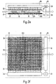
- Fig. 2a shows a section through an electric field generator/modulator according to the invention which functions as an electric patterning device for electric field-convertible materials.
- the electric field generator/modulator is realized such that it both generates the field and in addition also can modulate the fields spatially, i.e. in a plane or two-dimensions and generate electrical conducting and/or semiconducting structures with the desired pattern in this plane.
- EFGM 20 comprises as shown in fig. 2a in section and in fig. 2b in plan view a first electrode means E1, consisting of thin parallel electrodes 21 and another electrode means E2 provided spaced apart from the electrode means E1 in a plane parallel thereto.
- the electrode means E2 consists similarly of thin parallel electrodes 22 provided such that they are oriented substantially orthogonal to the electrodes 21 in the electrode means E1.
- the electrode means E1, E2 are connected with a power supply 23, here shown as a direct voltage supply, but the power supply 23 may also be an alternating voltage supply.
- the power supply 23 is connected with the electrode 21; 22 in the electrode means E1;E2 over respective cross-connecting devices 21, 24.
- the distance between the electrode means E1, E2 allows a thin film of electrical field-convertible material EFCM in fig. 2a denoted SS1 to be inserted between the electrode means E1, E2, without contacting these.
- the electrode means E1, E2 may be formed of self-supporting or supported thin films wherein the electrodes 21, 22 in each case are embedded in the film material.
- the layer SS1 of the field-convertible material EFCM may be a continuous tape which is inserted in EFGM 20 between the electrode means E1, E2 in a substantially continuous movement.
- an electrode 21 and another electrode 22 respectively are addressed electrically in this manner, an approximate point potential is obtained in the intersection between. If e.g. an electrode 21 in the electrode device E1 and all electrodes 22 in the electrode device E2 are addressed, a field is obtained substantially in the form of a line potential along the electrode 21 in question and correspondingly a line-like, for instance an electrical conducting structure in the layer SS1 which is located between the electrode devices E1, E2 will be generated.
- the field which are created between the electrode intersections will generate an area potential and it may for instance be generated an electric area structure in the layer SS1.
- such electrical conducting structures are e.g. generated substantially as area structures, but it is to be understood that there also may be generated as point of line structures, dependent on the manner whereby the electric field is generated.
- Figs. 2c and 2d show respectively in section and plan view how EFGM 20 is used for generating for instance electrical conducting structures 9 in a second layer by addressing the electrode means E1, E2 in EFGM 20 in a suitable manner.
- figs. 2e,f also shows in section and plan view EFGM 20 with a third layer SS3 which here for instance is patterned with semiconducting structures 10.
- the patterning of the field-convertible material EFCM takes place for each separate layer SS1, SS2, SS3, but these layers may as mentioned above, be present in the form of self-supporting single films of EFCM and assembled into a multilayer stack, such this schematically is shown in fig. 3.
- the fabrication of circuits realized with electrical conducting and/or semiconducting structures in EFCM can take place with tapes of EFCM in continuous paths as shown.
- Each tape or each film are in fig. 3 shown as three films EFCM1, EFCM2, EFCM3 and are converted by electric field to the desired spatial pattern in separate EFGM 20 for each of the paths.
- Then follows the assembly into a multilayer structure MLS, e.g. by gluing or heat-assisted lamination.
- the multilayer structure MLS may well be provided on a substrate which, of course, is not subjected to any electric field, but is laminated to the multilayer structure MLS in the same process step.
- a flexible tape MLS is obtained which either may be folded or coiled or cut into segments, for instance to make single circuits.
- the field-convertible material EFCM in the form of three tapes or films EFCM1, EFCM2, EFCM3 is drawn from respective rolls R a and conveyed in separate lines by alignment rolls R b1 , R b2 , P b3 , R b4 in each line for tensioning and positioning of the tapes through EFGM 20.
- the completed patterned films EFCM1, EFCM2, EFCM3 are conveyed over a guide roll set R c and possibly after a further position adjustment through a lamination step R d and laminated into the multilayer structure MLS.
- This multilayer structure may as mentioned, include a substrate 1 which is drawn from a further roll R a in a separate line and is laminated together with the converted film material EFCM in the lamination step R d .
- a substrate 1 which is drawn from a further roll R a in a separate line and is laminated together with the converted film material EFCM in the lamination step R d .
- it may then as shown schematically in section in fig. 4 be obtained a circuit structure which is provided on the substrate 1.
- the conducting structures 9 and the semiconducting structures 10 contact each other vertically or extend horizontally in each of the layers SS1, SS2, SS3 as shown and form to gether three-dimensional structures of this kind in the desired pattern.
- the electrode means E1, E2 in the electric field generator/modutalator (EFGM 20) as for instance shown in fig. 2a and fig. 2b, may be formed in or on substrates of a non-conducting material and the electrodes 21, 22 may then be provided on the opposite surfaces of the substrates or embedded in the substrates. They may also form conducting structures in the substrate material itself.
- the electrode width and the mutual distance between the electrodes 21, 22 in each electrode means E1, E2 will be determining for the spatial resolution in the patterning of the conducting and/or semiconducting structures and the achievable pitches. In compatibility with today's semiconductor technology the electrodes 21, 22 thus can be realized with a width between 0.1 and 1.0 ⁇ m and corresponding mutual distances.
- the circuit patterns which are realized with EFGM20 with the method according to the present invention will at least be dimensionally compatible with that which optimally may be achieved by using for instance microlithography in silicon-based circuit technology, Dependent on the thickness of thin film material wherein conducting and/or semiconducting structures, i.e. circuit patterns, shall be generated, the distance between the electrode devices E1, E2 can be controlled in order to achieve an optimum definition of the potentials formed between the electrodes. The control may take place via not shown micromechanical servocontrol means which are well-known to persons skilled in the art. - During the generation of the circuit pattern the space between the electrodes may besides be filled with an isolating gas with high dielectric strength in order to prevent break-down between the electrodes.
- the conversion can be performed with a high degree of reproducibility at well-defined field strength.
- the field strength necessary to induce the conversion will be in the order of 5 000 000 V/m, implying a potential difference over the electrode means E1, E2 in the order of 3-6 volts for film thicknesses in the 200-300 nm range and a gap between the electrode means E1, E2 large enough to accommodate films of this thickness.
- the electric field substantially is applied in a direction perpendicular to the thin film, although in principle it could be applied with other orientations. The former alternative appears as preferable with regard to the required precision in spatial resolution as well as obtaining a well-defined field strength.
- the power supply 23 in EFGM 20, e.g. as shown in fig. 2a and 2b, may either be a direct current source or an alternating current source.
- it will be realized as a controlled power supply and be able to supply the electrode means E1, E2 with current with different modes and characteristics.
- both the power supply 23 and the cross-connection means 24, 25 hence will be connected with a not shown external control device which may be programmed according to the protocol for a desired circuit pattern and corresponding control the generation of the desired electrical conducting and/or semiconducting structures in the layer material or the thin film material between the electrode means E1, E2. Protocols and required software may be loaded to the not shown control device from any external source and it is hence nothing against that the fabrication of circuits with the use of EFGM 20 may be managed from a distant locality.
- This material is an organometallic charge-transfer complex M(TCNQ) formed by TCNQ (7,7,8,8-tetracyanoquinodimetan, C 12 H 4 N 4 ) which functions as an electron acceptor molecule with different metals as electron-rich donors.
- the metals may be Li, Na, K, Ag, Cu or Fe.
- M(TCNQ) may under the application of electric fields and for the sake of that also energy supplied in the form of heat or light radiation transfer from a high impedance state to a low impedance state.
- the reaction can be written as M + ⁇ CNQ - n ⁇ ⁇ M x + TCNQ x h ⁇ , E ⁇ + M + ⁇ CNQ - n - x
- the process is reversible, as the return reaction may be obtained by supplying energy ⁇ in the form of heat, electrical fields or photon radiation.
- the reversible reaction results in that M(TCNQ) may be used for generating a bistable switching medium, for instance an erasable memory material.
- M(TCNQ) In the method according to the present invention only electric fields are used and not irradiation.
- M(TCNQ) has non-linear current-voltage characteristics, something which may be used for realizing memories of the type ROM and RAM. For this purpose it is of particular interest that M(TCNQ) stably and reproducably allows current-controlled bistable electrical switching.
- the high impedance state may be used for representing binary 1 and the low impedance state binary 0.
- the transition time between two such states is less than 400 ns.
- relevant materials are discussed in W. Xu & al., "Two new all-organic complexes with electrical bistable states", Appl. Phys. Lett. 67:2241-2242 (1995) and the therein appended literature references. The materials mentioned are bistable and have well-defined thresholds for conversion from conducting to non-conducting state and vice versa with the use of electric fields.
- the conversion from a non-conducting to a conducting state may also take place when the energy is supplied in the form of the heat.
- the field-convertible material basically is dielectric or strongly resistive, an electric alternating field which over the electrodes is applied with a suitable frequency to the material, may induce heat in the potential area and a heating with a subsequent conversion of the material from a non-conducting to a conducting state in this area may then take place.
- the power supply must then be operated as an alternating power supply and the thermal conversion must be regarded as a secondary effect induced by the electric field.
- the thermal field which is induced by the alternating field in the material must be precisely controlled.
- an alternating current pulse should be used which provides high field strength and a fast temperature increase in the potential area with subsequent rapid conversion of the field-convertible material. This may be achieved by combining a high field strength with high field frequency and with the use of field-convertible materials in the form of thin films with a thickness of 100 nm it is supposed that an unwanted thermal diffusion effectively can be avoided by using alternating current pulses of at most a few microseconds.
- the field characteristics must also be tuned to the desired degree of conductivity on the potential areas which ideally defines the generated conducting and/or semiconducting structures.
- connection as well as active and passive devices may be generated in the same processing sequence which defines the electrical conducting and/or semiconducting structures in each layer, i.e. with the same kind of spatial precision as the structures themselves and without resorting to further and other types of manufacturing steps.
- Fig. 5 shows the basic principle for the particular case where a single conducting path 9 shall be generated between a portion of for instance of a conducting structure in a layer SS5 and a portion of another conducting structure 9 in a layer SS8 spaced apart from the former.
- a column 9' of conducting material is formed as shown in fig.
- the cross-section of column 9' may be defined arbitrarily via the selected electric field pattern.
- a number of parallel conducting columns may be generated by direct extension of this procedure and the columns may begin and end in different layers such this is apparent from fig. 5.
- the latter shall be made concurrently with other conducting 9 and/or semiconducting structures 10 which are patterned in this layer, for instance SS6 in fig. 5, i.e. without having to carry out other or different processing steps.
- the degree of conversion from a non-conducting to a conducting state or vice versa can be controlled by the field strength and/or its time characteristics, possibly also by the duration of the field.
- a column which connects points in two different layers may be formed such that it functions as a resistor in a circuit by choosing the degree of conductivity in segments from layer to layer along the column.
- a method for erasing electrical conducting and/or semiconducting structures generated in three dimensions forms a part of the invention.
- electrical conducting and/or semiconducting structures in single layers be erased selectively with the use of EFGM20 as shown in any of the figs. 2a-f and suitable spectral modulation.
- the erasing at time being can, however, only be performed globally by the multilayer structure, in case the matrix, globally is subjected to an electric field with given field strength and/or characteristics and possibly adapted to the specific response of the material to the energy supplied by the field.
- the materials in the matrix will then be reconverted until the matrix in its entirety arrives in an electrical non-conducting state, something which will be the case if it e.g. is made of a material such as M(TCNQ).
- a multilayer structure or matrix of M(MTCNQ) material may thereafter be reconfigured with new electrical conducting and/or semiconducting structure, but this is not at present possible by using electrical fields.
- a method for generating as disclosed by the simultaneously filed International Patent Application PCT/NO99/00023 which belongs to the present applicant, may be used.
- suitable materials may be converted from an isolating to a semiconducting state or vice versa by electric fields, either directly or indirectly (e.g. in the last instance due to a simultaneous local heating), it will be possible to apply the method to manufacture for instance diodes and transistors which may be connected electrically with resistances and capacitors to form complete active electronic circuits. More specific examples of active components and circuits formed thereof shall be disclosed by the following examples.
- Fig. 6 shows a forward-biased pn junction diode with conducting and/or semiconducting structures generated by the method according the invention and realised in thin-film technology with four sublayers SS 1-SS4.
- the layers SS2 and SS3 contain the active semiconducting material provided between the electrodes 11 in respectively the sublayers SS1and SS4.
- the active material 10 in the sublayer SS2 is an n-doped semiconductor, while the adjacent active material 10' in the sublayer SS3 is a p-doped semiconductor.
- the electrodes 11 in the layers SS1 and SS4 are contacted by horizontal electrical conducting structures or conducting paths 9 in the same layer.
- the horizontal extension of the area of the diode structure will be determined by the spatial resolution which is realized with the use of an EFGM, but with the electrode means E1, E2 as shown in fig. 2a-f, it will be possible to form electrodes 21, 22 with pitches in the order of magnitude 0.2-1.0 ⁇ m by conventional lithographic methods or by using irradiation convertible materials and a method as disclosed in the above mentioned international patent application PCT/NO99/00023 . Special printing methods or use of nanotechnological and chemical methods will besides be able to realize electrode structures which are one order of magnitude smaller. Realistically it may be supposed that with the available technologies for making the electrode devices it will be possible to modulate point and line potentials spatially in two dimensions to a smallest extension of 0.1 ⁇ m.
- Fig. 7 shows schematically a MOSEET for use in the present invention and realized wholly in organic material in thin-film technology.
- the gate electrode 12 is provided in the sublayer SS1 and connected with a horizontal conducting structure 9, while the sublayer SS2 constitutes the gate isolator 13.
- the active semiconducting material 10 is provided in the sublayer SS3 and registers with the gate electrode 10.
- the source and drain electrodes 14 are provided in the following top layer SS4 and are contacted by horizontal electrical conducting structures 9 in the same layer.
- Each of the layers comprises either electrical conducting structures and/or a semiconducting structure, as well as dielectric areas.
- the thickness of a MOSFET of this kind may be 1 ⁇ 2 ⁇ m, while the extension in the horizontal plane such as may be realized with present technology will be from at most a few ⁇ m to less than 1 ⁇ m, cf. what is said in example 1.
- the MOSFET structure in fig. 7 may now be used in logic gates, for instance a logic inverter in CMOS technology as shown in fig. 8.
- An inverter of this kind is formed by parallel connection of the drain and source electrode in respectively an n-MOSFET and a p-MOSFET in a back-to-back configuration, with common gate electrode.
- a vertical conducting structure 15 is generated and passes through all sublayers SS1-SS7 and connects the electrodes 14'.
- the output signal from the inverter is conveyed on this conducting structure 15 to a horizontal connecting structure 9 at left in the figure.
- the common gate electrode 12 of the MOSFET receives the input signal via the horizontal conducting structure 9 in the sublayer SS4 at right in the figure.
- the thickness of all sublayers will then be less than 1 ⁇ m, typically realized with about a thickness of about 0.7 ⁇ m, while the horizontal extension of the inverter will have the same dimensions as stated above in connection with the discussion of the MOSFET structure in the
- Active components like the MOSFET structures shown in fig. 7 may be used for forming integrated circuits by stacking of sublayers with structures which have the desired electrical properties and wholly are realized in an organic thin-film technology.
- CMOS technology complementary MOS technology
- CMOS AND gate is realized with respectively n-MOSFETS and p-MOSFETS of the enrichment type as switches.
- Two input signals A and B are conveyed respectively to the gate electrodes on p-MOS Q 1 and Q 2 and the gate electrodes on n-MOS Q 3 and Q 4 . If both input signals switches A and B are high, the output signal X will be low. In this case Q 3 and Q 4 will both be on and the p-MOS switches Q 1 and Q 2 will both off, i.e. no current flows and the output signal X hence goes low. If, on the contrary, either the input signal A or the input signal B is low or both are low, correspondingly the p-MOS transistors Q 1 respectively Q 2 will be switched on and the output signal X goes high, as either one or both of the serially connected n-MOS Q 3 , Q 4 are off and no current flows.
- the devices Q 1 , Q 2 , Q 3 , Q 4 realize, as will be seen, a NAND gate and to realize an AND gate it is necessary to connect the output of the NAND gate with a logical inverter which also is realized in CMOS technology, respectively with the use of a p-MOS switch Q 2 and an n-MOS Q 6 switch connected in parallel.
- a logical inverter which also is realized in CMOS technology, respectively with the use of a p-MOS switch Q 2 and an n-MOS Q 6 switch connected in parallel.
- This is a standard CMOS inverter and if its input signal X is high, its output signal X will be the inverted of the input signal X and hence low. Conversely a low input signal X will be inverted to a high output signal X and this corresponds to the input signals A and B to the NAND gate both being high.
- circuit as shown in fig.
- Figs. 10a-10d show the AND gate wholly realized in thin-film technology and with the active and passive devices provided in four sublayers SS1, SS3-SS5.
- the first sublayer SS1 contains the gate electrodes g 1 -g 6 where the subscript points to the corresponding subscript for the MOSFETs Q 1 -Q 6 in fig. 9.
- the inputs A and B are conveyed to respectively the gate electrodes g 1 , g 3 and g 2 , g 4 and via horizontal conducting structures or current paths 9.
- the gate electrodes g 5 , g 6 in the inverter are connected with a horizontal current path 9.
- a vertical electrical conducting structure is denoted 15, the symbol ⁇ indicating that it extends upwards in vertical direction from the sublayers SS1.
- the symbols ⁇ and ⁇ indicate that the vertical conductor structure 15 in the laver SS3 extend vertically through this layer and on both sides thereof.
- the layer SS3 comprises areas with active semiconductor materials b 1 -b 6 (corresponding to 10 in fig. 7) which are assigned to and register with the corresponding gate electrodes g 1 -g 6 in the layer SS1.
- a layer SS2 exclusively, apart from the vertical conductor structure 15 which also extends through this sublayer on both sides thereof, consists of dielectric material which forms a common gate isolator for the MOSFETs Q 1 -Q 6 which realize the AND gate.
- the layer SS2 is, of course, located between SS1 and SS3, but has been excluded from the drawing.
- the layer SS4 fig. 10c is provided above and adjacent to the layer SS3 and comprises respectively the source electrodes S 1 -S 6 and the drain electrodes d 1 -d 6 for the corresponding MOSFETs Q 1 -Q 6 .
- the active semiconductor material d 1 -d 6 which is located in the layer SS3 is here indicated by stitched lines.
- the vertical current path 15 also extends also through the layer SS4 and to both sides thereof and contacts a horizontal current path 9 in the sublayer SS5 as shown in fig. 10d.
- This horizontal current path corresponds to the connection between the drain electrodes d 2 and d 3 for the corresponding MOSFETs Q 2 , Q 3 and is additionally also connected with the drain electrode d 1 on Q 1 .
- Another horizontal current path 9 realizes the serial connection between the source electrode s 3 on Q 3 and the drain electrode d 4 on Q 4 .
- the source electrodes s 4 and s 6 are grounded over further horizontal conductor structures 9, while the horizontal conducting structure 9 farthest to right in the layer SS5 is supplied with a voltage V dd and connects the source electrodes s 1 , s 2 , s 5 on respectively Q 1 , Q 2 and Q 5 .
- a further horizontal current path 9 uppermost in fig. 10d forms the parallel connection between the drain electrodes d 5 ,d 6 on Q 5 , Q 6 and the output line, denoted with X.
- the output signal X from the NAND gate consisting of Q 1 , Q 2 , Q 3 , Q 4 is conveyed on the vertical current path 15.
- Fig. 11 shows schematically how the layers in fig.
- the stack is shown exploded in its separate sublayers SS1-SS5, but with correct registration and the course of the vertical current path 15 through every sublayer is indicated by the stitched line.
- the total AND structure as shown in fig. 11 may have a thickness of 0.75 ⁇ m and an area of about 100 ⁇ m 2 (12 ⁇ 8 ⁇ m 2 ).
- the volume of the structure will hence be about 75 ⁇ m 3 .
- the length of the current paths 9, 15 together becomes 60 ⁇ m.
- Example 5 AND gate with vertically stacked CMOS circuits
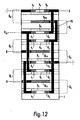
- a reduction of the current path length and a significant simplification of the structure of the AND gate may be achieved by stacking the MOSFET structures vertically as shown in fig. 12. Again the same reference numbers as in figs. 10 and 11 are used, and it will be seen that the vertical AND gate structure exploits the fact that the gate electrodes g 1 and g 3 of the transistors Q 1 , Q 3 are at the same common potential, the gate electrodes g 2 and g 4 in Q 2 , Q 4 on another common potential and the gate electrodes g 5 and g 5 in Q 3 , Q 6 on a third common potential.
- the transistors Q 1 -Q 6 are implemented as CMOS circuits in a pairwise back-to-back configuration by common gate electrode g 1 ,g 3 ; g 2 ,g 4 ; g 5 ,g 6 for the corresponding MOSFET structures Q 1 ,Q 3 ; Q 2 ,Q 4 ; Q 5 ,Q 6 .
- Each CMOS circuit is provided on an isolating layer which in fig. 12 is located below Q 3 , between Q 1 and Q 4 and between Q 2 and Q 5 in each of the MOSFET structures.
- the gate electrodes g are also, of course, isolated from the active semiconductor material b by not explicitly denoted isolating layers which comprise the respective gate isolators.
- the vertical AND gate structure in fig. 12 including the substrate 1 is generated by a total of 24 sublayers, of which 6 relatively thick isolating layers form the gate isolators and three corresponding thick isolating layers isolate the paired combinations of MOSFET structures mutually.
- the whole stacked layer configuration in fig. 12 hence will have a thickness of about 3.0 ⁇ m and be provided on an area of 16 ⁇ m 2 .
- the total volume thus becomes less than 50 ⁇ m 3 , a reduction of the volume of 1/3 relative to the configuration in fig. 11.
- the current paths which in the configuration in fig. 11 from the indicated dimensions will have a length of 52 ⁇ m, may in the configuration in fig.
- the configuration in fig. 11 may realize about 10 5 logic gates of the kind shown on 1 mm 2 and with a layer thickness well below 1 ⁇ m, while the configuration in fig. 12 might realize about 6 ⁇ 10 5 gates on the same area with a somewhat better form factor, such that the increase in the device density becomes about 33% relative to the device density of the configuration in fig. 11.
- the processing of single layers i.e. the generating of electrical conducting and/or semiconducting structures may after the converting by means of electric fields has taken place and when it is performed as shown in figs. 2a-f and fig. 3, include possible post-treatments and corrections, e.g. a possible heat treatment before the separate layers are joined into a multilayer structure and form a stacked circuit configuration.
- a heat treatment of single layers after the conversion may be performed to control conducting and/or semiconducting properties, e.g. conversion of monomer to oligomer or polymer, doping, crystallization etc.
- the heat treatment may e.g. be performed by means of irradiation.
- Another possibility is to use the electric alternating fields. In principle alternating fields may also be used to effect the field conversion of EFCM and the power supply 23 shown in figs. 2a-f must then, of course, be an alternating voltage source.
- a resistive material which is subjected to an alternating field will be heated.
- the protocol for a given circuit configuration in multilayer design may be generated far from the manufacturing location of the circuit and transmitted thereto for downloading to for instance a control device which controls the generation of the physical circuit patterns in situ at the manufacturing location.
- a user may hence thereby generate and produce circuits by tele-processing according to own specifications solely by transmitting the necessary instructions and information.
- the present invention may thus furnish the concept application- and customer-specific circuit production with a radically new content.
Landscapes
- Manufacturing & Machinery (AREA)
- Engineering & Computer Science (AREA)
- Thin Film Transistor (AREA)
- Semiconductor Memories (AREA)
- Metal-Oxide And Bipolar Metal-Oxide Semiconductor Integrated Circuits (AREA)
- Internal Circuitry In Semiconductor Integrated Circuit Devices (AREA)
- Testing Or Measuring Of Semiconductors Or The Like (AREA)
- Carbon And Carbon Compounds (AREA)
- Immobilizing And Processing Of Enzymes And Microorganisms (AREA)
- Electrical Discharge Machining, Electrochemical Machining, And Combined Machining (AREA)
- Prostheses (AREA)
- Secondary Cells (AREA)
- Electrodes Of Semiconductors (AREA)
- Contacts (AREA)
Claims (15)
- Verfahren zum Erzeugen elektrisch leitender und/oder halbleitender Strukturen in zwei oder drei Dimensionen in einer Verbundmatrix, wobei die Matrix ein oder mehrere Materialien umfaßt, die jeweils in einer oder mehreren räumlich getrennten und homogenen Materialstrukturen bereitgestellt sind, wobei die Materialien als Reaktion auf die Zufuhr von Energie spezifische Zustandsänderungen erfahren können, die einen Übergang von einem elektrisch nichtleitenden Zustand zu einem elektrisch leitenden und/oder halbleitenden Zustand oder umgekehrt oder eine Änderung bei dem Stromleitungsmodus des Materials verursachen und wobei jede Materialstruktur in der Form einer dünnen Schicht hergestellt ist,
gekennzeichnet durch Anlegen, an die getrennte Schicht, eines durch eine Potentialdifferenz erzeugten räumlich modulierten elektrischen Feldes mit einer gegebenen Feldstärke und/oder Charakteristik, ausgelegt für die spezifische Reaktion des Materials auf die von dem Feld gelieferte Energie, wobei das angelegte elektrische Feld entsprechend einem bestimmten Protokoll räumlich moduliert wird, das ein vorbestimmtes Muster elektrisch leitender und/oder nichtleitender Strukturen in der relevanten Materialstruktur darstellt, wodurch in den Schichten als Reaktion auf die von dem Feld gelieferte Energie zweidimensionale elektrisch leitende und/oder halbleitende Strukturen mit dem von dem Protokoll vorbestimmten Muster erzeugt werden, und dann wahlweise Bereitstellen von zwei oder mehr Schichten in einer gestapelten Konfiguration, so daß die von getrennten Schichten gebildete Verbundmatrix mit elektrisch leitenden und/oder halbleitenden Strukturen in drei Dimensionen versehen wird. - Verfahren nach Anspruch 1, gekennzeichnet durch räumliches Modulieren des durch eine Potentialdifferenz erzeugten elektrischen Feldes in einer Ebene im wesentlichen parallel mit einer Schicht mit Hilfe einer Elektrodeneinrichtung mit gemusterten Elektroden, wobei die Elektrodeneinrichtung durch selektive Zufuhr einer Spannung zu den Elektroden entsprechend dem bestimmten Protokoll elektrische Punkt- oder Linienpotentiale erzeugt, die die elektrisch leitenden und/oder halbleitenden Strukturen erzeugen.
- Verfahren nach Anspruch 1, dadurch gekennzeichnet, daß die gestapelte Konfiguration, ausgebildet durch zwei oder mehr Schichten nach dem Erzeugen der elektrisch leitenden und/oder halbleitenden Struktur in jeder Schicht, zu laminierten mehrschichtigen Strukturen kombiniert wird, was die Verbundmatrix mit elektrisch leitenden und/oder halbleitenden Strukturen in drei Dimensionen bildet.
- Verfahren nach Anspruch 3, gekennzeichnet durch das Ausbilden der Mehrfachschicht, ausgebildet durch eine Laminierung aus zwei oder mehr selbsttragenden Schichten, zu einer gestapelten Konfiguration.
- Verfahren nach Anspruch 4, gekennzeichnet durch das Positionieren einer Schicht nach der Laminierung zu benachbarten Schichten derart, daß zwei oder mehr zweidimensionale elektrisch leitende und/oder halbleitende Strukturen in der zuerst erwähnten Schicht gemäß dem Protokoll mit einer oder mehreren elektrisch leitenden und/oder halbleitenden Strukturen in benachbarten Schichten zusammenpassen, wodurch in der Querrichtung durch die Schichten ein oder mehrere vertikale elektrisch leitende und/oder halbleitende Kanäle erzeugt werden.
- Verfahren nach Anspruch 5, gekennzeichnet durch Bereitstellen einer elektrisch leitenden und/oder halbleitenden Struktur, die einen vertikalen Kanal durch die Schicht gemäß dem Protokoll bildet, in elektrisch leitender und/oder halbleitender Verbindung mit einer oder mehreren zweidimensionalen elektrisch leitenden und/oder halbleitenden Strukturen in dieser Schicht.
- Verfahren nach Anspruch 6, gekennzeichnet durch Erzeugen jedes Kanals mit einer Leitfähigkeit oder einem Leitungsmodus, die bzw. der zwischen den Schichten konstant ist.
- Verfahren nach Anspruch 6, gekennzeichnet durch Erzeugen jedes Kanals mit einer Leitfähigkeit oder einem Leitungsmodus, die bzw. der zwischen den Schichten variiert.
- Verfahren zum Löschen globaler, in zwei oder drei Dimensionen in einer Verbundmatrix erzeugter elektrisch leitender und/oder halbleitender Strukturen, wobei die Matrix ein oder mehrere Materialien umfaßt, die jeweils in einer oder mehreren räumlich getrennten und homogenen Materialstrukturen bereitgestellt sind, wobei die Materialien als Reaktion auf die Zufuhr von Energie spezifische Zustandsänderungen erfahren können, die einen Übergang von einem elektrisch nichtleitenden Zustand zu einem elektrisch leitenden und/oder halbleitenden Zustand oder umgekehrt oder eine Änderung bei dem Stromleitungsmodus des Materials verursachen und wobei jede Materialstruktur in der Form einer dünnen Schicht hergestellt ist,
gekennzeichnet durch globales Anlegen, an die Verbundmatrix, eines durch eine Potentialdifferenz erzeugten elektrischen Feldes mit einer gegebenen Feldstärke und/oder Charakteristik, ausgelegt für die spezifische Reaktion des Materials auf die von dem Feld gelieferte Energie, bis die Materialien in der Verbundmatrix als Reaktion auf die von dem Feld gelieferte Energie in ihrer Gänze in dem elektrisch nichtleitenden Zustand ankommen. - Elektrische-Feld-Generator/Modulator (EFGM) zum Strukturieren und Erzeugen elektrisch leitender und/oder halbleitender Strukturen in zwei oder drei Dimensionen in einer Verbundmatrix, wobei die Matrix ein oder mehrere Materialien umfaßt, die jeweils in einer oder mehreren räumlich getrennten und homogenen Materialstrukturen bereitgestellt sind, wobei die Materialien als Reaktion auf die zugeführte Energie spezifische Zustandsänderungen erfahren können, die einen Übergang von einem elektrisch nichtleitenden Zustand zu einem elektrisch leitenden und/oder halbleitenden Zustand und umgekehrt oder eine Änderung bei dem Leitungsmodus des Materials verursachen, wobei jede Materialstruktur in der Form einer dünnen Schicht hergestellt ist und wobei der Elektrische-Feld-Generator/Modulator (20) dadurch gekennzeichnet ist, daß er ein in einer Ebene bereitgestelltes erstes Elektrodenmittel (E1) mit mehreren parallelen Streifenelektroden (21), ein in einem Abstand von dem ersten Elektrodenmittel (E1) bereitgestelltes zweites Elektrodenmittel (E2) mit mehreren parallelen Streifenelektroden (22) und dazu in einer zweiten Ebene parallel zur ersten Ebene überlagert, so daß die Elektroden (21, 22) gegenseitig in einer matrixartigen Anordnung im wesentlichen orthogonal orientiert sind, daß die Elektrodenmittel (E1; E2) über Querverbindungseinrichtungen (24; 25) mit einer steuerbaren Stromversorgung (23) verbunden sind, der Elektrische-Feld-Generator/Modulator (20) in dem Raum zwischen den Elektrodenmitteln (E1, E2) ausgelegt ist, ein Dünnfilmmaterial in Form einer diskreten Komponente oder eines kontinuierlichen Bandes aufzunehmen, das ohne kontinuierliches oder intermittierendes Berühren der Elektrodenmittel durch den Raum mit gleichzeitiger Positionierung und Ausrichtung vorgeschoben wird, von den Elektrodenmittel (E1, E2) beanstandet und dazwischen in einer Ebene im wesentlichen parallel dazu, wodurch die elektrisch leitenden und/oder halbleitenden Strukturen erzeugt werden können gemäß einem bestimmten Protokoll und mit Hilfe von Punkt-, Linien- oder Flächenpotentialen, die zwischen ausgewählten Elektroden (21, 22) in den Elektrodenmitteln (E1; E2) erzeugt werden, wenn letztere über die Querverbindungseinrichtungen (24; 25) mit elektrischem Strom versorgt werden.
- Elektrische-Feld-Generator/Modulator nach Anspruch 10, dadurch gekennzeichnet, daß die Elektroden (21; 22) in jeder Elektrodeneinrichtung (E1; E2) an oder in Oberflächen von jeweiligen Substraten einander zugewandt vorgesehen sind.
- Elektrische-Feld-Generator/Modulator nach Anspruch 11, dadurch gekennzeichnet, daß die Streifenelektroden (21, 22) als Teil der Substrate hergestellt werden und leitende Strukturen in dem Substratmaterial bilden.
- Elektrische-Feld-Generator/Modulator nach Anspruch 10, dadurch gekennzeichnet, daß der Abstand zwischen den Elektrodenmitteln (E1, E2) je nach der Dicke des Dünnfilmmaterials gesteuert werden kann.
- Elektrische-Feld-Generator/Modulator nach Anspruch 10, dadurch gekennzeichnet, daß die Elektroden (21; 22) in jedem Elektrodenmittel (E1; E2) mit einem gegenseitigen Abstand zwischen 0,1 µm und 1,0 µm vorgesehen sind.
- Elektrische-Feld-Generator/Modulator nach Anspruch 10, dadurch gekennzeichnet, daß die Elektroden (21; 22) in jedem Elektrodenmittel (E1; E2) mit einer im wesentlichen konstanten Breite von 0,1 µm und 1,0 µm vorgesehen sind.
Applications Claiming Priority (5)
| Application Number | Priority Date | Filing Date | Title |
|---|---|---|---|
| NO980385 | 1998-01-28 | ||
| NO980385A NO980385D0 (no) | 1998-01-28 | 1998-01-28 | Kretser generert ved omvandling in situ |
| NO982518 | 1998-06-02 | ||
| NO982518A NO308149B1 (no) | 1998-06-02 | 1998-06-02 | Skalerbar, integrert databehandlingsinnretning |
| PCT/NO1999/000022 WO1999044229A1 (en) | 1998-01-28 | 1999-01-28 | A method for generating electrical conducting or semiconducting structures in two or three dimensions, a method for erasing the same structures and an electric field generator/modulator for use with the method for generating |
Publications (2)
| Publication Number | Publication Date |
|---|---|
| EP1051745A1 EP1051745A1 (de) | 2000-11-15 |
| EP1051745B1 true EP1051745B1 (de) | 2007-11-07 |
Family
ID=26648814
Family Applications (2)
| Application Number | Title | Priority Date | Filing Date |
|---|---|---|---|
| EP99907966A Expired - Lifetime EP1051745B1 (de) | 1998-01-28 | 1999-01-28 | Methode zur herstellung zwei- oder dreidimensionaler elektrisch leitender oder halbleitender strukturen, eine löschmethode derselben und ein generator/modulator eines elektrischen feldes zum gebrauch in der herstellungsmethode |
| EP99902942A Withdrawn EP1051741A1 (de) | 1998-01-28 | 1999-01-28 | Herstellung und zerstörung dreidimensionaler, leitender oder halbleitender strukturen |
Family Applications After (1)
| Application Number | Title | Priority Date | Filing Date |
|---|---|---|---|
| EP99902942A Withdrawn EP1051741A1 (de) | 1998-01-28 | 1999-01-28 | Herstellung und zerstörung dreidimensionaler, leitender oder halbleitender strukturen |
Country Status (11)
| Country | Link |
|---|---|
| US (3) | US6403396B1 (de) |
| EP (2) | EP1051745B1 (de) |
| JP (2) | JP4272353B2 (de) |
| KR (2) | KR100375392B1 (de) |
| CN (2) | CN1187793C (de) |
| AT (1) | ATE377842T1 (de) |
| AU (2) | AU739848B2 (de) |
| CA (2) | CA2319430C (de) |
| DE (1) | DE69937485T2 (de) |
| RU (2) | RU2210834C2 (de) |
| WO (2) | WO1999044229A1 (de) |
Families Citing this family (144)
| Publication number | Priority date | Publication date | Assignee | Title |
|---|---|---|---|---|
| US6859548B2 (en) | 1996-09-25 | 2005-02-22 | Kabushiki Kaisha Toshiba | Ultrasonic picture processing method and ultrasonic picture processing apparatus |
| US6839158B2 (en) | 1997-08-28 | 2005-01-04 | E Ink Corporation | Encapsulated electrophoretic displays having a monolayer of capsules and materials and methods for making the same |
| US6842657B1 (en) | 1999-04-09 | 2005-01-11 | E Ink Corporation | Reactive formation of dielectric layers and protection of organic layers in organic semiconductor device fabrication |
| US7030412B1 (en) | 1999-05-05 | 2006-04-18 | E Ink Corporation | Minimally-patterned semiconductor devices for display applications |
| WO2001007961A1 (en) | 1999-07-21 | 2001-02-01 | E Ink Corporation | Use of a storage capacitor to enhance the performance of an active matrix driven electronic display |
| US6545291B1 (en) | 1999-08-31 | 2003-04-08 | E Ink Corporation | Transistor design for use in the construction of an electronically driven display |
| WO2001033649A1 (en) * | 1999-11-02 | 2001-05-10 | Koninklijke Philips Electronics N.V. | Method of producing vertical interconnects between thin film microelectronic devices and products comprising such vertical interconnects |
| DE19964099B4 (de) * | 1999-12-31 | 2006-04-06 | Götzen, Reiner, Dipl.-Ing. | Verfahren zur Herstellung dreidimensional angeordneter Leit- und Verbindungsstrukturen für Volumen- und Energieströme |
| EP1136942A1 (de) * | 2000-03-22 | 2001-09-26 | Infineon Technologies AG | Schaltungsanordnung zum Schützen einer Schaltung gegen Analyse und Manipulation |
| US7893435B2 (en) | 2000-04-18 | 2011-02-22 | E Ink Corporation | Flexible electronic circuits and displays including a backplane comprising a patterned metal foil having a plurality of apertures extending therethrough |
| DE60139463D1 (de) | 2000-04-18 | 2009-09-17 | E Ink Corp | Prozess zur herstellung von dünnfilmtransistoren |
| US20040029310A1 (en) * | 2000-08-18 | 2004-02-12 | Adoft Bernds | Organic field-effect transistor (ofet), a production method therefor, an integrated circut constructed from the same and their uses |
| WO2002015264A2 (de) * | 2000-08-18 | 2002-02-21 | Siemens Aktiengesellschaft | Verkapseltes organisch-elektronisches bauteil, verfahren zu seiner herstellung und seine verwendung |
| KR100394028B1 (ko) * | 2000-12-28 | 2003-08-06 | 엘지.필립스 엘시디 주식회사 | 액정표시장치 및 그 제조방법 |
| DE10043204A1 (de) * | 2000-09-01 | 2002-04-04 | Siemens Ag | Organischer Feld-Effekt-Transistor, Verfahren zur Strukturierung eines OFETs und integrierte Schaltung |
| DE10044842A1 (de) * | 2000-09-11 | 2002-04-04 | Siemens Ag | Organischer Gleichrichter, Schaltung, RFID-Tag und Verwendung eines organischen Gleichrichters |
| US20040026121A1 (en) * | 2000-09-22 | 2004-02-12 | Adolf Bernds | Electrode and/or conductor track for organic components and production method thereof |
| DE10061297C2 (de) * | 2000-12-08 | 2003-05-28 | Siemens Ag | Verfahren zur Sturkturierung eines OFETs |
| DE10061299A1 (de) * | 2000-12-08 | 2002-06-27 | Siemens Ag | Vorrichtung zur Feststellung und/oder Weiterleitung zumindest eines Umwelteinflusses, Herstellungsverfahren und Verwendung dazu |
| DE10063721A1 (de) * | 2000-12-20 | 2002-07-11 | Merck Patent Gmbh | Organischer Halbleiter, Herstellungsverfahren dazu und Verwendungen |
| DE10105914C1 (de) * | 2001-02-09 | 2002-10-10 | Siemens Ag | Organischer Feldeffekt-Transistor mit fotostrukturiertem Gate-Dielektrikum und ein Verfahren zu dessen Erzeugung |
| US20040094771A1 (en) * | 2001-03-26 | 2004-05-20 | Adolf Bernds | Device with at least two organic electronic components and method for producing the same |
| EP1390984B1 (de) | 2001-05-07 | 2009-08-26 | Advanced Micro Devices, Inc. | Floating-gate-speicherbaustein, der zusammengesetztes molekularmaterial verwendet |
| CN100367528C (zh) * | 2001-05-07 | 2008-02-06 | 先进微装置公司 | 具储存效应的开关装置 |
| AU2002340793A1 (en) * | 2001-05-07 | 2002-11-18 | Coatue Corporation | Molecular memory device |
| WO2002091496A2 (en) | 2001-05-07 | 2002-11-14 | Advanced Micro Devices, Inc. | Reversible field-programmable electric interconnects |
| WO2002091385A1 (en) * | 2001-05-07 | 2002-11-14 | Advanced Micro Devices, Inc. | Molecular memory cell |
| CN100403450C (zh) * | 2001-05-07 | 2008-07-16 | 先进微装置公司 | 具有自组装聚合物薄膜的内存装置及其制造方法 |
| US6756620B2 (en) * | 2001-06-29 | 2004-06-29 | Intel Corporation | Low-voltage and interface damage-free polymer memory device |
| WO2003009359A1 (fr) * | 2001-07-16 | 2003-01-30 | Boris Aronovich Gurovich | Procede de formation d'une structure a couches multiples a parametres predetermines |
| US6624457B2 (en) | 2001-07-20 | 2003-09-23 | Intel Corporation | Stepped structure for a multi-rank, stacked polymer memory device and method of making same |
| US6967640B2 (en) | 2001-07-27 | 2005-11-22 | E Ink Corporation | Microencapsulated electrophoretic display with integrated driver |
| US6768157B2 (en) | 2001-08-13 | 2004-07-27 | Advanced Micro Devices, Inc. | Memory device |
| US6858481B2 (en) | 2001-08-13 | 2005-02-22 | Advanced Micro Devices, Inc. | Memory device with active and passive layers |
| US6806526B2 (en) | 2001-08-13 | 2004-10-19 | Advanced Micro Devices, Inc. | Memory device |
| CN100419906C (zh) | 2001-08-13 | 2008-09-17 | 先进微装置公司 | 存储器单元 |
| US6838720B2 (en) * | 2001-08-13 | 2005-01-04 | Advanced Micro Devices, Inc. | Memory device with active passive layers |
| DE10151036A1 (de) * | 2001-10-16 | 2003-05-08 | Siemens Ag | Isolator für ein organisches Elektronikbauteil |
| DE10151440C1 (de) | 2001-10-18 | 2003-02-06 | Siemens Ag | Organisches Elektronikbauteil, Verfahren zu seiner Herstellung und seine Verwendung |
| DE10160732A1 (de) * | 2001-12-11 | 2003-06-26 | Siemens Ag | Organischer Feld-Effekt-Transistor mit verschobener Schwellwertspannung und Verwendung dazu |
| KR100433407B1 (ko) * | 2002-02-06 | 2004-05-31 | 삼성광주전자 주식회사 | 업라이트형 진공청소기 |
| US6900851B2 (en) | 2002-02-08 | 2005-05-31 | E Ink Corporation | Electro-optic displays and optical systems for addressing such displays |
| DE10212640B4 (de) * | 2002-03-21 | 2004-02-05 | Siemens Ag | Logische Bauteile aus organischen Feldeffekttransistoren |
| DE10212639A1 (de) * | 2002-03-21 | 2003-10-16 | Siemens Ag | Vorrichtung und Verfahren zur Laserstrukturierung von Funktionspolymeren und Verwendungen |
| RU2205469C1 (ru) * | 2002-04-18 | 2003-05-27 | Гурович Борис Аронович | Способ получения объемной проводящей структуры |
| RU2205470C1 (ru) * | 2002-05-07 | 2003-05-27 | Гурович Борис Аронович | Способ формирования структуры |
| DE10226370B4 (de) * | 2002-06-13 | 2008-12-11 | Polyic Gmbh & Co. Kg | Substrat für ein elektronisches Bauteil, Verwendung des Substrates, Verfahren zur Erhöhung der Ladungsträgermobilität und Organischer Feld-Effekt Transistor (OFET) |
| US6661024B1 (en) * | 2002-07-02 | 2003-12-09 | Motorola, Inc. | Integrated circuit including field effect transistor and method of manufacture |
| WO2004017439A2 (de) * | 2002-07-29 | 2004-02-26 | Siemens Aktiengesellschaft | Elektronisches bauteil mit vorwiegend organischen funktionsmaterialien und herstellungsverfahren dazu |
| US20060079327A1 (en) * | 2002-08-08 | 2006-04-13 | Wolfgang Clemens | Electronic device |
| CN100338791C (zh) | 2002-08-23 | 2007-09-19 | 波尔伊克两合公司 | 用于过电压保护的有机元件及相关电路 |
| US7012276B2 (en) * | 2002-09-17 | 2006-03-14 | Advanced Micro Devices, Inc. | Organic thin film Zener diodes |
| EP1559147B1 (de) * | 2002-10-02 | 2014-11-12 | Leonhard Kurz Stiftung & Co. KG | Folie mit organischen halbleitern |
| RU2222847C1 (ru) * | 2002-10-21 | 2004-01-27 | Государственное предприятие "Центр технологий микроэлектроники" | Наносенсорная система |
| US6870183B2 (en) | 2002-11-04 | 2005-03-22 | Advanced Micro Devices, Inc. | Stacked organic memory devices and methods of operating and fabricating |
| EP1559148A2 (de) * | 2002-11-05 | 2005-08-03 | Siemens Aktiengesellschaft | ORGANISCHES ELEKTRONISCHES BAUTEIL MIT HOCHAUFGELöSTER STRUKTURIERUNG UND HERSTELLUNGSVERFAHREN DAZU |
| DE10253154A1 (de) * | 2002-11-14 | 2004-05-27 | Siemens Ag | Messgerät zur Bestimmung eines Analyten in einer Flüssigkeitsprobe |
| DE50306538D1 (de) * | 2002-11-19 | 2007-03-29 | Polyic Gmbh & Co Kg | Organische elektronische schaltung mit stukturierter halbleitender funktionsschicht und herstellungsverfahren dazu |
| US20060035423A1 (en) * | 2002-11-19 | 2006-02-16 | Walter Fix | Organic electronic component comprising the same organic material for at least two functional layers |
| US6905908B2 (en) * | 2002-12-26 | 2005-06-14 | Motorola, Inc. | Method of fabricating organic field effect transistors |
| DE10300521A1 (de) * | 2003-01-09 | 2004-07-22 | Siemens Ag | Organoresistiver Speicher |
| DE10394193D2 (de) * | 2003-01-17 | 2005-12-01 | Agnes Goetzen | Verfahren zur Herstellung von Mikrosystemen |
| DE10302149A1 (de) * | 2003-01-21 | 2005-08-25 | Siemens Ag | Verwendung leitfähiger Carbon-black/Graphit-Mischungen für die Herstellung von low-cost Elektronik |
| WO2004066348A2 (de) * | 2003-01-21 | 2004-08-05 | Polyic Gmbh & Co. Kg | Organisches elektronikbauteil und verfahren zur herstellung organischer elektronik |
| MXPA05007878A (es) * | 2003-01-29 | 2006-02-08 | Polylc Gmbh & Co Kg | Unidad de memoria organica y circuito impulsor para la misma. |
| JP2004311845A (ja) * | 2003-04-09 | 2004-11-04 | National Institute Of Advanced Industrial & Technology | 発電機能を有する可視光透過構造体 |
| US7049153B2 (en) | 2003-04-23 | 2006-05-23 | Micron Technology, Inc. | Polymer-based ferroelectric memory |
| JP4583004B2 (ja) * | 2003-05-21 | 2010-11-17 | 株式会社 日立ディスプレイズ | アクティブ・マトリクス基板の製造方法 |
| DE10330062A1 (de) * | 2003-07-03 | 2005-01-27 | Siemens Ag | Verfahren und Vorrichtung zur Strukturierung von organischen Schichten |
| DE10330064B3 (de) * | 2003-07-03 | 2004-12-09 | Siemens Ag | Logikgatter mit potentialfreier Gate-Elektrode für organische integrierte Schaltungen |
| RU2243613C1 (ru) * | 2003-07-16 | 2004-12-27 | Гурович Борис Аронович | Способ формирования объемной структуры |
| DE10338277A1 (de) * | 2003-08-20 | 2005-03-17 | Siemens Ag | Organischer Kondensator mit spannungsgesteuerter Kapazität |
| DE10339036A1 (de) | 2003-08-25 | 2005-03-31 | Siemens Ag | Organisches elektronisches Bauteil mit hochaufgelöster Strukturierung und Herstellungsverfahren dazu |
| DE10340644B4 (de) * | 2003-09-03 | 2010-10-07 | Polyic Gmbh & Co. Kg | Mechanische Steuerelemente für organische Polymerelektronik |
| DE10340643B4 (de) * | 2003-09-03 | 2009-04-16 | Polyic Gmbh & Co. Kg | Druckverfahren zur Herstellung einer Doppelschicht für Polymerelektronik-Schaltungen, sowie dadurch hergestelltes elektronisches Bauelement mit Doppelschicht |
| EP1665406A1 (de) * | 2003-09-24 | 2006-06-07 | E.I. Dupont De Nemours And Company | Prozess zum laminieren einer dielektrischen schicht auf einen halbleiter |
| JP4729843B2 (ja) * | 2003-10-15 | 2011-07-20 | 凸版印刷株式会社 | 薄膜トランジスタの製造方法 |
| DE10349963A1 (de) | 2003-10-24 | 2005-06-02 | Leonhard Kurz Gmbh & Co. Kg | Verfahren zur Herstellung einer Folie |
| DE102004002024A1 (de) * | 2004-01-14 | 2005-08-11 | Siemens Ag | Organischer Transistor mit selbstjustierender Gate-Elektrode und Verfahren zu dessen Herstellung |
| JP4501444B2 (ja) * | 2004-02-04 | 2010-07-14 | ソニー株式会社 | トランジスタにおける配線構造の形成方法及び電界効果型トランジスタの製造方法 |
| WO2005104210A2 (en) | 2004-04-20 | 2005-11-03 | Visualsonics Inc. | Arrayed ultrasonic transducer |
| US7122489B2 (en) * | 2004-05-12 | 2006-10-17 | Matsushita Electric Industrial Co., Ltd. | Manufacturing method of composite sheet material using ultrafast laser pulses |
| US7374102B2 (en) * | 2004-05-14 | 2008-05-20 | Wavezero, Inc. | Radiofrequency antennae and identification tags and methods of manufacturing radiofrequency antennae and radiofrequency identification tags |
| US7019328B2 (en) * | 2004-06-08 | 2006-03-28 | Palo Alto Research Center Incorporated | Printed transistors |
| GB0413749D0 (en) * | 2004-06-19 | 2004-07-21 | Koninkl Philips Electronics Nv | Active matrix electronic array device |
| DE102004040831A1 (de) * | 2004-08-23 | 2006-03-09 | Polyic Gmbh & Co. Kg | Funketikettfähige Umverpackung |
| RU2284267C2 (ru) * | 2004-11-10 | 2006-09-27 | Броня Цой | Материал для компонентов радиоэлектронных приборов |
| DE102004059465A1 (de) * | 2004-12-10 | 2006-06-14 | Polyic Gmbh & Co. Kg | Erkennungssystem |
| DE102004059467A1 (de) * | 2004-12-10 | 2006-07-20 | Polyic Gmbh & Co. Kg | Gatter aus organischen Feldeffekttransistoren |
| DE102004059464A1 (de) * | 2004-12-10 | 2006-06-29 | Polyic Gmbh & Co. Kg | Elektronikbauteil mit Modulator |
| DE102004063435A1 (de) | 2004-12-23 | 2006-07-27 | Polyic Gmbh & Co. Kg | Organischer Gleichrichter |
| DE102005009820A1 (de) * | 2005-03-01 | 2006-09-07 | Polyic Gmbh & Co. Kg | Elektronikbaugruppe mit organischen Logik-Schaltelementen |
| DE102005009819A1 (de) | 2005-03-01 | 2006-09-07 | Polyic Gmbh & Co. Kg | Elektronikbaugruppe |
| DE102005017655B4 (de) * | 2005-04-15 | 2008-12-11 | Polyic Gmbh & Co. Kg | Mehrschichtiger Verbundkörper mit elektronischer Funktion |
| KR100719346B1 (ko) * | 2005-04-19 | 2007-05-17 | 삼성전자주식회사 | 저항 메모리 셀, 그 형성 방법 및 이를 이용한 저항 메모리배열 |
| US7420442B1 (en) * | 2005-06-08 | 2008-09-02 | Sandia Corporation | Micromachined microwave signal control device and method for making same |
| NO20052904L (no) * | 2005-06-14 | 2006-12-15 | Thin Film Electronics Asa | Et ikke-flyktig elektrisk minnesystem |
| DE102005031448A1 (de) | 2005-07-04 | 2007-01-11 | Polyic Gmbh & Co. Kg | Aktivierbare optische Schicht |
| EP1742226B1 (de) * | 2005-07-08 | 2010-09-15 | STMicroelectronics Srl | Verfahren zur Realisierung einer elektrischen Verbindung in einer elektronischen Halbleitervorrichtung zwischen einem nanometrischen Schaltungsarchitektur und elektronischen Standardkomponenten |
| DE102005035589A1 (de) | 2005-07-29 | 2007-02-01 | Polyic Gmbh & Co. Kg | Verfahren zur Herstellung eines elektronischen Bauelements |
| DE102005035590A1 (de) * | 2005-07-29 | 2007-02-01 | Polyic Gmbh & Co. Kg | Elektronisches Bauelement |
| DE102005042166A1 (de) * | 2005-09-06 | 2007-03-15 | Polyic Gmbh & Co.Kg | Organisches Bauelement und ein solches umfassende elektrische Schaltung |
| DE102005044306A1 (de) * | 2005-09-16 | 2007-03-22 | Polyic Gmbh & Co. Kg | Elektronische Schaltung und Verfahren zur Herstellung einer solchen |
| CA2628100C (en) | 2005-11-02 | 2016-08-23 | Visualsonics Inc. | High frequency array ultrasound system |
| RU2302054C1 (ru) * | 2006-02-16 | 2007-06-27 | Борис Аронович Гурович | Способ создания пространственно-объемной структуры |
| JP2007252249A (ja) * | 2006-03-22 | 2007-10-04 | Oki Electric Ind Co Ltd | 有機化合物合成装置,光照射装置,有機化合物合成用基板および有機化合物の合成方法 |
| US20070279230A1 (en) * | 2006-06-01 | 2007-12-06 | Wavezero, Inc. | System and Method for Attaching Radiofrequency Identification Chips to Metalized Antenna |
| JP2008021814A (ja) * | 2006-07-13 | 2008-01-31 | Hitachi Ltd | 電界効果トランジスタ、有機薄膜トランジスタおよび有機トランジスタの製造方法 |
| TWI300251B (en) * | 2006-07-14 | 2008-08-21 | Ind Tech Res Inst | Manufacturing method of vertical thin film transistor |
| US7851786B2 (en) * | 2006-09-01 | 2010-12-14 | Alcatel-Lucent Usa Inc. | Programmable polyelectrolyte electrical switches |
| RU2332746C1 (ru) * | 2006-12-25 | 2008-08-27 | Юрий Александрович Савиных | Способ формирования равномерного электрического поля в электропроводной среде |
| JP5250981B2 (ja) * | 2007-02-21 | 2013-07-31 | セイコーエプソン株式会社 | 有機デバイスの製造方法並びに電子機器 |
| WO2009067577A1 (en) * | 2007-11-21 | 2009-05-28 | The Board Of Trustees Of The Leland Stanford Junior University. | Patterning of organic semiconductor materials |
| RU2363068C1 (ru) * | 2008-01-30 | 2009-07-27 | Федеральное Государственное учреждение "Российский научный центр "Курчатовский институт" (РНЦ "Курчатовский институт") | Способ формирования композиционной структуры |
| US9184369B2 (en) | 2008-09-18 | 2015-11-10 | Fujifilm Sonosite, Inc. | Methods for manufacturing ultrasound transducers and other components |
| US8316518B2 (en) * | 2008-09-18 | 2012-11-27 | Visualsonics Inc. | Methods for manufacturing ultrasound transducers and other components |
| US9173047B2 (en) | 2008-09-18 | 2015-10-27 | Fujifilm Sonosite, Inc. | Methods for manufacturing ultrasound transducers and other components |
| US10441185B2 (en) * | 2009-12-16 | 2019-10-15 | The Board Of Trustees Of The University Of Illinois | Flexible and stretchable electronic systems for epidermal electronics |
| KR20120103651A (ko) * | 2009-12-23 | 2012-09-19 | 아이엠알에이 아메리카, 인코포레이티드. | 구조화된 광학 요소 및 포커싱된 빔을 이용하는 레이저 패터닝 |
| US9196509B2 (en) | 2010-02-16 | 2015-11-24 | Deca Technologies Inc | Semiconductor device and method of adaptive patterning for panelized packaging |
| US8656333B1 (en) * | 2010-02-16 | 2014-02-18 | Deca Technologies, Inc. | Integrated circuit package auto-routing |
| US8799845B2 (en) | 2010-02-16 | 2014-08-05 | Deca Technologies Inc. | Adaptive patterning for panelized packaging |
| US8502159B2 (en) * | 2010-04-29 | 2013-08-06 | Battelle Energy Alliance, Llc | Apparatuses and methods for generating electric fields |
| US20110266436A1 (en) * | 2010-04-29 | 2011-11-03 | Battelle Energy Alliance, Llc | Apparatuses and methods for forming electromagnetic fields |
| RU2461151C1 (ru) * | 2011-01-25 | 2012-09-10 | Федеральное государственное автономное образовательное учреждение высшего профессионального образования "Национальный исследовательский ядерный университет "МИФИ" (НИЯУ МИФИ) | Ионный диод для генерации нейтронов |
| RU2479890C1 (ru) * | 2011-12-07 | 2013-04-20 | Открытое акционерное общество "Научно-исследовательский институт полупроводникового машиностроения" | Кассета для технологических спутников фотопреобразователей |
| JP6105266B2 (ja) | 2011-12-15 | 2017-03-29 | 株式会社半導体エネルギー研究所 | 記憶装置 |
| SG11201504940RA (en) | 2012-01-23 | 2015-07-30 | Semiconductor Energy Lab | Semiconductor device |
| JP2013161878A (ja) * | 2012-02-02 | 2013-08-19 | Renesas Electronics Corp | 半導体装置、および半導体装置の製造方法 |
| US8753904B2 (en) * | 2012-06-07 | 2014-06-17 | Taiwan Semiconductor Manufacturing Company, Ltd. | Method and system for semiconductor device pattern loading effect characterization |
| US9482518B2 (en) | 2012-06-07 | 2016-11-01 | Taiwan Semiconductor Manufacturing Company, Ltd. | Systems and methods for semiconductor device process determination using reflectivity measurement |
| RU2504046C1 (ru) * | 2012-07-12 | 2014-01-10 | Открытое акционерное общество "Концерн радиостроения "Вега" | Способ получения межсоединений в высокоплотных электронных модулях |
| CN103338596A (zh) * | 2013-06-18 | 2013-10-02 | 华南理工大学 | 一种不用光刻胶的全加成线路板制作方法 |
| US9040316B1 (en) | 2014-06-12 | 2015-05-26 | Deca Technologies Inc. | Semiconductor device and method of adaptive patterning for panelized packaging with dynamic via clipping |
| CN104282250B (zh) * | 2014-10-24 | 2016-08-31 | 深圳市华星光电技术有限公司 | Tft 中mis 结构设计的控制方法及系统 |
| JP6504497B2 (ja) * | 2015-03-04 | 2019-04-24 | 株式会社アルバック | タッチパネルおよび透明導電性基板 |
| CN105353590B (zh) * | 2015-12-11 | 2018-01-02 | 中国电子科技集团公司第四十一研究所 | 薄膜电路金属化孔内光刻胶的曝光方法及基片承载装置 |
| US10573601B2 (en) | 2016-09-19 | 2020-02-25 | Deca Technologies Inc. | Semiconductor device and method of unit specific progressive alignment |
| US10157803B2 (en) | 2016-09-19 | 2018-12-18 | Deca Technologies Inc. | Semiconductor device and method of unit specific progressive alignment |
| US10482976B2 (en) * | 2017-06-29 | 2019-11-19 | SK Hynix Inc. | Memory device performing UV-assisted erase operation |
| RU185725U1 (ru) * | 2018-07-02 | 2018-12-17 | федеральное государственное бюджетное научное учреждение "Научно-исследовательский институт перспективных материалов и технологий" | Микроволновое устройство для термообработки полимерных композиционных материалов |
| RU2700231C1 (ru) * | 2018-10-24 | 2019-09-13 | Федеральное государственное автономное образовательное учреждение высшего образования "Национальный исследовательский университет "Московский институт электронной техники" | Способ формирования трехмерных структур топологических элементов функциональных слоев на поверхности подложек |
| EP3953739A1 (de) * | 2019-04-12 | 2022-02-16 | Queen Mary University of London | Strahlungsdetektor |
| CN116801532A (zh) * | 2021-05-14 | 2023-09-22 | Oppo广东移动通信有限公司 | 壳体、其制备方法、可穿戴设备及电子设备 |
Citations (1)
| Publication number | Priority date | Publication date | Assignee | Title |
|---|---|---|---|---|
| US5677041A (en) * | 1993-03-25 | 1997-10-14 | Texas Instruments Incorporated | Integrated circuits formed in radiation sensitive material and method of forming same |
Family Cites Families (29)
| Publication number | Priority date | Publication date | Assignee | Title |
|---|---|---|---|---|
| US4371883A (en) * | 1980-03-14 | 1983-02-01 | The Johns Hopkins University | Current controlled bistable electrical organic thin film switching device |
| US4507672A (en) * | 1980-03-14 | 1985-03-26 | The Johns Hopkins University | Method of fabricating a current controlled bistable electrical organic thin film switching device |
| US5407851A (en) | 1981-02-23 | 1995-04-18 | Unisys Corporation | Method of fabricating an electrically alterable resistive component on an insulating layer above a semiconductor substrate |
| US4825408A (en) * | 1984-04-25 | 1989-04-25 | The Johns Hopkins University | Multistate optical switching and memory apparatus using an amphoteric organic charge transfer material |
| IL86162A (en) * | 1988-04-25 | 1991-11-21 | Zvi Orbach | Customizable semiconductor devices |
| US5427941A (en) | 1985-08-08 | 1995-06-27 | Schering Corporation | Actinomadura brunnea var. antibiotica strains |
| KR900008647B1 (ko) * | 1986-03-20 | 1990-11-26 | 후지쓰 가부시끼가이샤 | 3차원 집적회로와 그의 제조방법 |
| EP0263574A1 (de) * | 1986-09-08 | 1988-04-13 | THORN EMI North America Inc. | Methode zur Herstellung eines Halbleiterbauelementes und ein solches Bauelement mit zumindest einer selektiv aktivierbaren Leiterbahn |
| US4806995A (en) * | 1987-02-02 | 1989-02-21 | Olin Corporation | Optical and electrical switching devices and a polymer composition containing pendant organic charge transfer salt moieties useful in switching devices |
| EP0344346B1 (de) * | 1988-06-01 | 1995-04-26 | Texas Instruments Incorporated | Optische Schaltvorrichtung |
| SU1729243A1 (ru) * | 1988-12-01 | 1995-11-10 | Н.И. Татаренко | Способ изготовления тонкопленочного вакуумного микроприбора |
| SU1616439A1 (ru) * | 1989-02-03 | 1996-01-20 | Д.М. Боднарь | Способ создания многоуровневых межсоединений интегральных схем |
| JPH07103190B2 (ja) * | 1989-02-15 | 1995-11-08 | 松下電器産業株式会社 | 有機導電性薄膜とその製造方法 |
| US5043251A (en) * | 1989-11-29 | 1991-08-27 | The United States Of America As Represented By The Secretary Of The Navy | Process of three dimensional lithography in amorphous polymers |
| SU1795821A1 (ru) * | 1990-05-18 | 1995-10-10 | Казанский физико-технический институт Казанского научного центра АН СССР | Способ получения мезотаксиальных слоев дисилицида кобальта в кремнии |
| US5689428A (en) * | 1990-09-28 | 1997-11-18 | Texas Instruments Incorporated | Integrated circuits, transistors, data processing systems, printed wiring boards, digital computers, smart power devices, and processes of manufacture |
| SU1826815A1 (ru) * | 1991-05-16 | 1995-03-27 | Минский радиотехнический институт | Способ рекристаллизации кремниевых слоев |
| US5282312A (en) * | 1991-12-31 | 1994-02-01 | Tessera, Inc. | Multi-layer circuit construction methods with customization features |
| US5378916A (en) * | 1993-02-17 | 1995-01-03 | Xerox Corporation | Color imaging charge-coupled array with multiple photosensitive regions |
| US5427841A (en) | 1993-03-09 | 1995-06-27 | U.S. Philips Corporation | Laminated structure of a metal layer on a conductive polymer layer and method of manufacturing such a structure |
| ATE171560T1 (de) | 1993-03-09 | 1998-10-15 | Koninkl Philips Electronics Nv | Herstellungsverfahren eines musters von einem elektrisch leitfähigen polymer auf einer substratoberfläche und metallisierung eines solchen musters |
| JPH09503622A (ja) | 1993-09-30 | 1997-04-08 | コピン・コーポレーシヨン | 転写薄膜回路を使用した3次元プロセッサー |
| US5537108A (en) * | 1994-02-08 | 1996-07-16 | Prolinx Labs Corporation | Method and structure for programming fuses |
| US5572409A (en) * | 1994-02-08 | 1996-11-05 | Prolinx Labs Corporation | Apparatus including a programmable socket adapter for coupling an electronic component to a component socket on a printed circuit board |
| US5808351A (en) * | 1994-02-08 | 1998-09-15 | Prolinx Labs Corporation | Programmable/reprogramable structure using fuses and antifuses |
| JP3770631B2 (ja) * | 1994-10-24 | 2006-04-26 | 株式会社ルネサステクノロジ | 半導体装置の製造方法 |
| RU2107973C1 (ru) * | 1996-03-20 | 1998-03-27 | Омский государственный университет | Способ формирования многослойных структур с разными электрофизическими свойствами |
| US5703394A (en) * | 1996-06-10 | 1997-12-30 | Motorola | Integrated electro-optical package |
| EP0968537B1 (de) * | 1997-08-22 | 2012-05-02 | Creator Technology B.V. | Feld-effekt-transistor, der im wesentlichen aus organischen materialien besteht |
-
1999
- 1999-01-28 AU AU23032/99A patent/AU739848B2/en not_active Ceased
- 1999-01-28 CN CNB998044903A patent/CN1187793C/zh not_active Expired - Fee Related
- 1999-01-28 WO PCT/NO1999/000022 patent/WO1999044229A1/en not_active Ceased
- 1999-01-28 KR KR10-2000-7008287A patent/KR100375392B1/ko not_active Expired - Fee Related
- 1999-01-28 EP EP99907966A patent/EP1051745B1/de not_active Expired - Lifetime
- 1999-01-28 CA CA002319430A patent/CA2319430C/en not_active Expired - Fee Related
- 1999-01-28 DE DE69937485T patent/DE69937485T2/de not_active Expired - Fee Related
- 1999-01-28 KR KR10-2000-7008278A patent/KR100375864B1/ko not_active Expired - Fee Related
- 1999-01-28 EP EP99902942A patent/EP1051741A1/de not_active Withdrawn
- 1999-01-28 AT AT99907966T patent/ATE377842T1/de not_active IP Right Cessation
- 1999-01-28 AU AU27495/99A patent/AU733522B2/en not_active Ceased
- 1999-01-28 WO PCT/NO1999/000023 patent/WO1999045582A1/en not_active Ceased
- 1999-01-28 JP JP2000533897A patent/JP4272353B2/ja not_active Expired - Fee Related
- 1999-01-28 RU RU2000122454/28A patent/RU2210834C2/ru not_active IP Right Cessation
- 1999-01-28 US US09/381,995 patent/US6403396B1/en not_active Expired - Fee Related
- 1999-01-28 CN CNB998044377A patent/CN1171301C/zh not_active Expired - Fee Related
- 1999-01-28 RU RU2000122445/28A patent/RU2183882C2/ru not_active IP Right Cessation
- 1999-01-28 CA CA002319428A patent/CA2319428C/en not_active Expired - Fee Related
- 1999-01-28 US US09/381,994 patent/US6432739B1/en not_active Expired - Fee Related
- 1999-01-28 JP JP2000535041A patent/JP2002515641A/ja active Pending
-
2001
- 2001-10-17 US US09/978,043 patent/US6776806B2/en not_active Expired - Fee Related
Patent Citations (1)
| Publication number | Priority date | Publication date | Assignee | Title |
|---|---|---|---|---|
| US5677041A (en) * | 1993-03-25 | 1997-10-14 | Texas Instruments Incorporated | Integrated circuits formed in radiation sensitive material and method of forming same |
Also Published As
Similar Documents
| Publication | Publication Date | Title |
|---|---|---|
| US6432739B1 (en) | Method for generating electrical conducting or semiconducting structures in two or three dimensions, a method for erasing the same structures and an electric field generator/modulator for use with the method for generating | |
| US6552409B2 (en) | Techniques for addressing cross-point diode memory arrays | |
| KR101547326B1 (ko) | 트랜지스터 및 그 제조방법 | |
| Bock | Polymer electronics systems-polytronics | |
| KR100368819B1 (ko) | 판독-전용 메모리 및 판독-전용 메모리 장치 | |
| JP2002518848A (ja) | 拡張性集積データ処理装置 | |
| JP2001244424A5 (de) | ||
| TW200527601A (en) | Self assembly of conducting polymer for formation of polymer memory cell | |
| JP2008527690A (ja) | メモリ・デバイス製造方法 | |
| KR20070085953A (ko) | 유기 전계 효과 트랜지스터 게이트 | |
| US20080048188A1 (en) | Electronic devices integrated on a single substrate and method for fabricating the same | |
| KR100473970B1 (ko) | 메모리 소자 및 그 제조방법 | |
| WO2005122233A1 (ja) | ショットキーゲート有機電界効果トランジスタおよびその製造方法 | |
| HK1035438B (en) | A method for generating a method for erasing electrical conducting or semiconducting structures, and an electric field generator/modulator | |
| HK1035602B (en) | A method for generation of electrical conducting or semiconducting structures in three dimensions and methods for erasure of the same structures |
Legal Events
| Date | Code | Title | Description |
|---|---|---|---|
| PUAI | Public reference made under article 153(3) epc to a published international application that has entered the european phase |
Free format text: ORIGINAL CODE: 0009012 |
|
| 17P | Request for examination filed |
Effective date: 20000825 |
|
| AK | Designated contracting states |
Kind code of ref document: A1 Designated state(s): AT BE CH DE DK ES FI FR GB IE IT LI NL PT SE |
|
| 17Q | First examination report despatched |
Effective date: 20040825 |
|
| GRAP | Despatch of communication of intention to grant a patent |
Free format text: ORIGINAL CODE: EPIDOSNIGR1 |
|
| GRAS | Grant fee paid |
Free format text: ORIGINAL CODE: EPIDOSNIGR3 |
|
| GRAA | (expected) grant |
Free format text: ORIGINAL CODE: 0009210 |
|
| AK | Designated contracting states |
Kind code of ref document: B1 Designated state(s): AT BE CH DE DK ES FI FR GB IE IT LI NL PT SE |
|
| REG | Reference to a national code |
Ref country code: GB Ref legal event code: FG4D |
|
| REG | Reference to a national code |
Ref country code: IE Ref legal event code: FG4D |
|
| REG | Reference to a national code |
Ref country code: CH Ref legal event code: EP |
|
| REF | Corresponds to: |
Ref document number: 69937485 Country of ref document: DE Date of ref document: 20071220 Kind code of ref document: P |
|
| PG25 | Lapsed in a contracting state [announced via postgrant information from national office to epo] |
Ref country code: SE Free format text: LAPSE BECAUSE OF FAILURE TO SUBMIT A TRANSLATION OF THE DESCRIPTION OR TO PAY THE FEE WITHIN THE PRESCRIBED TIME-LIMIT Effective date: 20080207 Ref country code: NL Free format text: LAPSE BECAUSE OF FAILURE TO SUBMIT A TRANSLATION OF THE DESCRIPTION OR TO PAY THE FEE WITHIN THE PRESCRIBED TIME-LIMIT Effective date: 20071107 Ref country code: LI Free format text: LAPSE BECAUSE OF FAILURE TO SUBMIT A TRANSLATION OF THE DESCRIPTION OR TO PAY THE FEE WITHIN THE PRESCRIBED TIME-LIMIT Effective date: 20071107 Ref country code: ES Free format text: LAPSE BECAUSE OF FAILURE TO SUBMIT A TRANSLATION OF THE DESCRIPTION OR TO PAY THE FEE WITHIN THE PRESCRIBED TIME-LIMIT Effective date: 20080218 Ref country code: CH Free format text: LAPSE BECAUSE OF FAILURE TO SUBMIT A TRANSLATION OF THE DESCRIPTION OR TO PAY THE FEE WITHIN THE PRESCRIBED TIME-LIMIT Effective date: 20071107 |
|
| NLV1 | Nl: lapsed or annulled due to failure to fulfill the requirements of art. 29p and 29m of the patents act | ||
| REG | Reference to a national code |
Ref country code: CH Ref legal event code: PL |
|
| ET | Fr: translation filed | ||
| PG25 | Lapsed in a contracting state [announced via postgrant information from national office to epo] |
Ref country code: AT Free format text: LAPSE BECAUSE OF FAILURE TO SUBMIT A TRANSLATION OF THE DESCRIPTION OR TO PAY THE FEE WITHIN THE PRESCRIBED TIME-LIMIT Effective date: 20071107 |
|
| PG25 | Lapsed in a contracting state [announced via postgrant information from national office to epo] |
Ref country code: DK Free format text: LAPSE BECAUSE OF FAILURE TO SUBMIT A TRANSLATION OF THE DESCRIPTION OR TO PAY THE FEE WITHIN THE PRESCRIBED TIME-LIMIT Effective date: 20071107 |
|
| PG25 | Lapsed in a contracting state [announced via postgrant information from national office to epo] |
Ref country code: BE Free format text: LAPSE BECAUSE OF FAILURE TO SUBMIT A TRANSLATION OF THE DESCRIPTION OR TO PAY THE FEE WITHIN THE PRESCRIBED TIME-LIMIT Effective date: 20071107 |
|
| PLBE | No opposition filed within time limit |
Free format text: ORIGINAL CODE: 0009261 |
|
| STAA | Information on the status of an ep patent application or granted ep patent |
Free format text: STATUS: NO OPPOSITION FILED WITHIN TIME LIMIT |
|
| PG25 | Lapsed in a contracting state [announced via postgrant information from national office to epo] |
Ref country code: PT Free format text: LAPSE BECAUSE OF FAILURE TO SUBMIT A TRANSLATION OF THE DESCRIPTION OR TO PAY THE FEE WITHIN THE PRESCRIBED TIME-LIMIT Effective date: 20080407 |
|
| 26N | No opposition filed |
Effective date: 20080808 |
|
| PG25 | Lapsed in a contracting state [announced via postgrant information from national office to epo] |
Ref country code: IE Free format text: LAPSE BECAUSE OF NON-PAYMENT OF DUE FEES Effective date: 20080128 |
|
| PG25 | Lapsed in a contracting state [announced via postgrant information from national office to epo] |
Ref country code: FI Free format text: LAPSE BECAUSE OF FAILURE TO SUBMIT A TRANSLATION OF THE DESCRIPTION OR TO PAY THE FEE WITHIN THE PRESCRIBED TIME-LIMIT Effective date: 20071107 |
|
| PGFP | Annual fee paid to national office [announced via postgrant information from national office to epo] |
Ref country code: DE Payment date: 20090112 Year of fee payment: 11 |
|
| PGFP | Annual fee paid to national office [announced via postgrant information from national office to epo] |
Ref country code: GB Payment date: 20090112 Year of fee payment: 11 |
|
| PGFP | Annual fee paid to national office [announced via postgrant information from national office to epo] |
Ref country code: FR Payment date: 20090107 Year of fee payment: 11 |
|
| GBPC | Gb: european patent ceased through non-payment of renewal fee |
Effective date: 20100128 |
|
| REG | Reference to a national code |
Ref country code: FR Ref legal event code: ST Effective date: 20100930 |
|
| PG25 | Lapsed in a contracting state [announced via postgrant information from national office to epo] |
Ref country code: FR Free format text: LAPSE BECAUSE OF NON-PAYMENT OF DUE FEES Effective date: 20100201 |
|
| PG25 | Lapsed in a contracting state [announced via postgrant information from national office to epo] |
Ref country code: DE Free format text: LAPSE BECAUSE OF NON-PAYMENT OF DUE FEES Effective date: 20100803 |
|
| PG25 | Lapsed in a contracting state [announced via postgrant information from national office to epo] |
Ref country code: GB Free format text: LAPSE BECAUSE OF NON-PAYMENT OF DUE FEES Effective date: 20100128 |
|
| PG25 | Lapsed in a contracting state [announced via postgrant information from national office to epo] |
Ref country code: IT Free format text: LAPSE BECAUSE OF NON-PAYMENT OF DUE FEES Effective date: 20080131 |