EP1052695A2 - Support à bande et methode de fabrication d'un dispositif semi-conducteur de type support à bande - Google Patents
Support à bande et methode de fabrication d'un dispositif semi-conducteur de type support à bande Download PDFInfo
- Publication number
- EP1052695A2 EP1052695A2 EP00302918A EP00302918A EP1052695A2 EP 1052695 A2 EP1052695 A2 EP 1052695A2 EP 00302918 A EP00302918 A EP 00302918A EP 00302918 A EP00302918 A EP 00302918A EP 1052695 A2 EP1052695 A2 EP 1052695A2
- Authority
- EP
- European Patent Office
- Prior art keywords
- tape carrier
- type semiconductor
- wiring patterns
- tape
- carrier type
- Prior art date
- Legal status (The legal status is an assumption and is not a legal conclusion. Google has not performed a legal analysis and makes no representation as to the accuracy of the status listed.)
- Withdrawn
Links
Images



Classifications
-
- H—ELECTRICITY
- H10—SEMICONDUCTOR DEVICES; ELECTRIC SOLID-STATE DEVICES NOT OTHERWISE PROVIDED FOR
- H10W—GENERIC PACKAGES, INTERCONNECTIONS, CONNECTORS OR OTHER CONSTRUCTIONAL DETAILS OF DEVICES COVERED BY CLASS H10
- H10W90/00—Package configurations
-
- H—ELECTRICITY
- H05—ELECTRIC TECHNIQUES NOT OTHERWISE PROVIDED FOR
- H05K—PRINTED CIRCUITS; CASINGS OR CONSTRUCTIONAL DETAILS OF ELECTRIC APPARATUS; MANUFACTURE OF ASSEMBLAGES OF ELECTRICAL COMPONENTS
- H05K3/00—Apparatus or processes for manufacturing printed circuits
- H05K3/0011—Working of insulating substrates or insulating layers
- H05K3/0044—Mechanical working of the substrate, e.g. drilling or punching
- H05K3/0052—Depaneling, i.e. dividing a panel into circuit boards; Working of the edges of circuit boards
-
- H—ELECTRICITY
- H10—SEMICONDUCTOR DEVICES; ELECTRIC SOLID-STATE DEVICES NOT OTHERWISE PROVIDED FOR
- H10W—GENERIC PACKAGES, INTERCONNECTIONS, CONNECTORS OR OTHER CONSTRUCTIONAL DETAILS OF DEVICES COVERED BY CLASS H10
- H10W70/00—Package substrates; Interposers; Redistribution layers [RDL]
- H10W70/60—Insulating or insulated package substrates; Interposers; Redistribution layers
- H10W70/67—Insulating or insulated package substrates; Interposers; Redistribution layers characterised by their insulating layers or insulating parts
- H10W70/688—Flexible insulating substrates
-
- H—ELECTRICITY
- H10—SEMICONDUCTOR DEVICES; ELECTRIC SOLID-STATE DEVICES NOT OTHERWISE PROVIDED FOR
- H10W—GENERIC PACKAGES, INTERCONNECTIONS, CONNECTORS OR OTHER CONSTRUCTIONAL DETAILS OF DEVICES COVERED BY CLASS H10
- H10W72/00—Interconnections or connectors in packages
- H10W72/01—Manufacture or treatment
- H10W72/0198—Manufacture or treatment batch processes
-
- H—ELECTRICITY
- H05—ELECTRIC TECHNIQUES NOT OTHERWISE PROVIDED FOR
- H05K—PRINTED CIRCUITS; CASINGS OR CONSTRUCTIONAL DETAILS OF ELECTRIC APPARATUS; MANUFACTURE OF ASSEMBLAGES OF ELECTRICAL COMPONENTS
- H05K1/00—Printed circuits
- H05K1/02—Details
- H05K1/11—Printed elements for providing electric connections to or between printed circuits
- H05K1/117—Pads along the edge of rigid circuit boards, e.g. for pluggable connectors
-
- H—ELECTRICITY
- H05—ELECTRIC TECHNIQUES NOT OTHERWISE PROVIDED FOR
- H05K—PRINTED CIRCUITS; CASINGS OR CONSTRUCTIONAL DETAILS OF ELECTRIC APPARATUS; MANUFACTURE OF ASSEMBLAGES OF ELECTRICAL COMPONENTS
- H05K2203/00—Indexing scheme relating to apparatus or processes for manufacturing printed circuits covered by H05K3/00
- H05K2203/15—Position of the PCB during processing
- H05K2203/1545—Continuous processing, i.e. involving rolls moving a band-like or solid carrier along a continuous production path
-
- H—ELECTRICITY
- H10—SEMICONDUCTOR DEVICES; ELECTRIC SOLID-STATE DEVICES NOT OTHERWISE PROVIDED FOR
- H10W—GENERIC PACKAGES, INTERCONNECTIONS, CONNECTORS OR OTHER CONSTRUCTIONAL DETAILS OF DEVICES COVERED BY CLASS H10
- H10W72/00—Interconnections or connectors in packages
- H10W72/071—Connecting or disconnecting
- H10W72/073—Connecting or disconnecting of die-attach connectors
-
- H—ELECTRICITY
- H10—SEMICONDUCTOR DEVICES; ELECTRIC SOLID-STATE DEVICES NOT OTHERWISE PROVIDED FOR
- H10W—GENERIC PACKAGES, INTERCONNECTIONS, CONNECTORS OR OTHER CONSTRUCTIONAL DETAILS OF DEVICES COVERED BY CLASS H10
- H10W72/00—Interconnections or connectors in packages
- H10W72/071—Connecting or disconnecting
- H10W72/073—Connecting or disconnecting of die-attach connectors
- H10W72/07331—Connecting techniques
-
- H—ELECTRICITY
- H10—SEMICONDUCTOR DEVICES; ELECTRIC SOLID-STATE DEVICES NOT OTHERWISE PROVIDED FOR
- H10W—GENERIC PACKAGES, INTERCONNECTIONS, CONNECTORS OR OTHER CONSTRUCTIONAL DETAILS OF DEVICES COVERED BY CLASS H10
- H10W72/00—Interconnections or connectors in packages
- H10W72/30—Die-attach connectors
- H10W72/321—Structures or relative sizes of die-attach connectors
- H10W72/325—Die-attach connectors having a filler embedded in a matrix
-
- H—ELECTRICITY
- H10—SEMICONDUCTOR DEVICES; ELECTRIC SOLID-STATE DEVICES NOT OTHERWISE PROVIDED FOR
- H10W—GENERIC PACKAGES, INTERCONNECTIONS, CONNECTORS OR OTHER CONSTRUCTIONAL DETAILS OF DEVICES COVERED BY CLASS H10
- H10W72/00—Interconnections or connectors in packages
- H10W72/30—Die-attach connectors
- H10W72/351—Materials of die-attach connectors
-
- H—ELECTRICITY
- H10—SEMICONDUCTOR DEVICES; ELECTRIC SOLID-STATE DEVICES NOT OTHERWISE PROVIDED FOR
- H10W—GENERIC PACKAGES, INTERCONNECTIONS, CONNECTORS OR OTHER CONSTRUCTIONAL DETAILS OF DEVICES COVERED BY CLASS H10
- H10W72/00—Interconnections or connectors in packages
- H10W72/30—Die-attach connectors
- H10W72/351—Materials of die-attach connectors
- H10W72/352—Materials of die-attach connectors comprising metals or metalloids, e.g. solders
-
- H—ELECTRICITY
- H10—SEMICONDUCTOR DEVICES; ELECTRIC SOLID-STATE DEVICES NOT OTHERWISE PROVIDED FOR
- H10W—GENERIC PACKAGES, INTERCONNECTIONS, CONNECTORS OR OTHER CONSTRUCTIONAL DETAILS OF DEVICES COVERED BY CLASS H10
- H10W74/00—Encapsulations, e.g. protective coatings
- H10W74/10—Encapsulations, e.g. protective coatings characterised by their shape or disposition
- H10W74/15—Encapsulations, e.g. protective coatings characterised by their shape or disposition on active surfaces of flip-chip devices, e.g. underfills
-
- H—ELECTRICITY
- H10—SEMICONDUCTOR DEVICES; ELECTRIC SOLID-STATE DEVICES NOT OTHERWISE PROVIDED FOR
- H10W—GENERIC PACKAGES, INTERCONNECTIONS, CONNECTORS OR OTHER CONSTRUCTIONAL DETAILS OF DEVICES COVERED BY CLASS H10
- H10W90/00—Package configurations
- H10W90/701—Package configurations characterised by the relative positions of pads or connectors relative to package parts
- H10W90/721—Package configurations characterised by the relative positions of pads or connectors relative to package parts of bump connectors
- H10W90/724—Package configurations characterised by the relative positions of pads or connectors relative to package parts of bump connectors between a chip and a stacked insulating package substrate, interposer or RDL
-
- H—ELECTRICITY
- H10—SEMICONDUCTOR DEVICES; ELECTRIC SOLID-STATE DEVICES NOT OTHERWISE PROVIDED FOR
- H10W—GENERIC PACKAGES, INTERCONNECTIONS, CONNECTORS OR OTHER CONSTRUCTIONAL DETAILS OF DEVICES COVERED BY CLASS H10
- H10W90/00—Package configurations
- H10W90/701—Package configurations characterised by the relative positions of pads or connectors relative to package parts
- H10W90/731—Package configurations characterised by the relative positions of pads or connectors relative to package parts of die-attach connectors
- H10W90/734—Package configurations characterised by the relative positions of pads or connectors relative to package parts of die-attach connectors between a chip and a stacked insulating package substrate, interposer or RDL
Definitions
- the present invention relates to a tape carrier type semiconductor device composed of a flexible printed board and a semiconductor element bonded and mounted thereon, and a method of manufacturing the same.
- TAB Tape Automated Bonding
- Tape carrier type semiconductor devices obtained by the TAB technique include a COF (Chip On FPC (Flexible Printed Circuit)), a TCP (Tape Carrier Package), etc.
- COF Chip On FPC
- TCP Transmission Carrier Package
- the tape carrier is bonded to the semiconductor element electrode and a wiring pattern on the bonded portion is backed with a tape carrier material.
- the TCP the tape carrier material is bonded to the semiconductor element electrode and a through-hole is provided in the bonded portion where the semiconductor element is mounted. Further, a top end of a wiring pattern called an inner lead which protrudes to form a cantilever is bonded to the semiconductor element electrode.
- the tape carrier type semiconductor devices are mainly used as a liquid crystal driver, a thermal head printer, etc.
- the tape carrier type semiconductor device is completed in the following manner. That is, identical wiring patterns are formed successively on a lengthy tape (tape carrier material) at regular intervals in a single direction with respect to a direction in which the tape is fed, and semiconductor elements are mounted at specific positions of the wiring patterns. Then, the tape carrier type semiconductor device is completed when punched out individually from the lengthy tape.
- the tape carrier type semiconductor devices formed on the tape carrier are designed along a single direction with respect to a direction in which the tape is fed.
- the tape carrier type semiconductor device thus completed is used for a liquid crystal panel, for example, it is connected to the liquid crystal panel at one side end, and to the printed board or the like at the other side end.
- each tape carrier type semiconductor device is not necessarily a rectangle, which is a shape the area of the tape carrier is utilized efficiently, and can be of an L-shape, a T-shape, a triangular shape, etc.
- the tape carrier When the manufacturing procedure and used materials of the tape carrier are concerned, the tape carrier is manufactured in the form of a lengthy tape from reel to reel, and therefore, the cost thereof increases in proportion to the tape area. Thus, even if some areas of the tape carrier are not used in manufacturing the tape carrier semiconductor devices, the cost wasted on such areas is included in the manufacturing cost. Therefore, the manufacturing cost of the tape carrier type semiconductor devices increases as the areas which are not used in manufacturing the same increases. The useless areas may be reduced by designing the tape carrier type semiconductor devices in a shape with which the tape carrier is utilized efficiently (for example, rectangles). However, this is not preferable, because the design flexibility given to the tape carrier type semiconductor devices as benefits will be lost.
- Japanese Laid-open Utility Model No. 82852/1994 Japanese Laid-open Utility Model No. 82852/1994 (Japanese Official Gazette Jitsukaihei No. 6-82852 , publishing date: November 25, 1994) discloses a technique for aligning the semiconductor device TABs in more than one row in the width direction of the tape carrier as a method of minimizing unused areas on the tape carrier and conducting an electrical test on more than one TAB simultaneously.
- the above publication does not solve the problem that useless areas are readily formed on the tape area if the tape carrier type semiconductor devices are of arbitrary shapes, because each TAB is aligned in one specific direction with respect to a direction in which the tape is fed, and each TAB is of a rectangular shape with which the tape area can be utilized efficiently.
- a tape carrier of the present invention is a tape carrier used for a tape carrier type semiconductor device comprising a lengthy tape carrier and a semiconductor element bonded and mounted thereon, on which wiring patterns of the tape carrier type semiconductor device are successively formed, in which:
- a tape carrier type semiconductor device of the present invention is manufactured by:
- a manufacturing method of a tape carrier type semiconductor device of the present invention includes:
- the above tape carrier, tape carrier type semiconductor device, and manufacturing method of the tape carrier type semiconductor device by aligning the wiring patterns of the identical shape in more than one direction with respect to a direction in which the tape carrier is fed in a layout such that increases a utilized area of the tape carrier, useless areas which have no contribution in forming the tape carrier type semiconductor devices on the tape carrier can be reduced compared with a conventional arrangement in which all the wiring patterns are formed and aligned on the tape carrier along the same direction.
- a tape carrier of the present invention is a tape carrier used for a tape carrier type semiconductor device comprising a lengthy tape carrier and a semiconductor element bonded and mounted thereon, on which wiring patterns of the tape carrier type semiconductor device are successively formed, in which:
- a tape carrier type semiconductor device of the present invention is manufactured by:
- a method of manufacturing a tape carrier type semiconductor device of the present invention includes:
- the wiring patterns of more than one kind each having a different shape are aligned on the same tape carrier
- these wiring patterns of more than one kind can be aligned in a layout such that increases a utilized area of the tape carrier by making an optimal combination.
- useless areas which have no contribution in forming the tape carrier type semiconductor devices on the tape carrier can be reduced compared with the conventional arrangement in which the wiring patterns of the same kind are aligned along the same direction.
- tape carrier type semiconductor devices of more than one kind are manufactured, these tape carrier type semiconductor devices can be manufactured simultaneously on a single kind of tape carrier.
- the arrangements of the present invention are suitable in manufacturing the devices of many kinds with a small number of each.
- the wiring patterns of more than one kind each having a different shape include mirror symmetrical wiring patterns.
- the tape carrier type semiconductor devices of the present invention include COFs, TCPs, etc., and because substantially the same functional effect can be attained whether the present invention is applied to the COFs or TCPs, the kinds of the tape carrier type semiconductor devices of the present invention are not especially limited. It should be appreciated, however, that because the COFs are not shaped in rectangles in many cases in comparison with the TCPs, the present invention can be more appreciated with the COFs. Thus, in the following explanation, the COFs are used as examples of the tape carrier type semiconductor devices. The COFs are not precisely defined, and those mounted on the tape and those punched out individually from the tape are both referred to as the COFs.
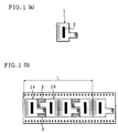
- Figures 1(a) and 1(b) show the shape of the COF of the present embodiment and the layout of the COF patterns on the tape carrier, respectively.
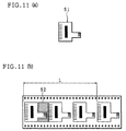
- a COF 1 is of the shape shown in Figure 1(a), which is identical with the shape of the COF 51 shown in Figure 11(a).
- the COF 1 is composed of a flexible printed board on which a wiring pattern has been formed, and a semiconductor element (indicated by black-paint) 2 bonded and mounted thereon.
- the wiring pattern is generally composed of an inner lead connected to the electrode of the semiconductor element 2 and an outer lead connected to an external circuit. In Figure 1(a), the inner lead is omitted for ease of explanation.
- the COFs 1 are designed in a layout so as to be aligned on the tape carrier in accordance with the method of the present embodiment, adjacent COF patterns 1a and 1b are positioned on the tape carrier in such a manner that one is turned by 180 degrees with respect to the other. When punched out from the tape carrier, the COFs 1 of the identical shape can be obtained from the COF patterns 1a and 1b.
- a useless area 52 is formed as all the COFs 51 are aligned in a single direction, and three COFs 51 are manufactured out of the tape carrier of a specific length L.
- a useless area 3 is formed as well, but it is quite small compared with the useless area 52, and four COFs 1 are manufactured out of the tape carrier of the same length L.
- four COFs are manufactured out of the tape carrier of the same length L.
- four COFs are manufactured in the present embodiment whereas three COFs are manufactured in the conventional arrangement.
- Figure 2 shows a cross section of the COF 1.
- the semiconductor element 2 is bonded onto the tape carrier 4 at a specific position, and a space formed between the tape carrier 4 and semiconductor element 2 is filled with sealing resin 5.
- the tape carrier 4 is composed of an insulating material (tape carrier material) 6 made of polyimide, and a copper foil pattern (wiring pattern ) 8 layered thereon through a bonding agent 7 having a thickness of 5-15 ⁇ m.
- the thickness of the insulating material 6 is 75 ⁇ m (typical thickness of an ordinary TCP), 40 ⁇ m, or 25 ⁇ m.
- the thickness of 40 ⁇ m or 25 ⁇ m is preferable to fully exploit the flexibility of the COF given as benefits.
- a protruding electrode (generally referred to as bump) 9 is formed at an external outlet electrode of the semiconductor element 2. Tinning or gilding is applied to the copper foil pattern 8 and protruding electrode 9 when necessary, and in the present embodiment, tinning is applied to the copper toil pattern 8 and gilding is applied to the protruding electrode 9.
- the semiconductor element 2 and tape carrier 4 are positioned in such a manner that the electrode forming surface of the former opposes the pattern surface of the latter, and heat and pressure are applied for a predetermined time from either the back surface of the electrode forming surface of the semiconductor element 2 or the back surface of the pattern surface of the tape carrier 4, whereby the protruding electrode 9 of the semiconductor element 2 is connected to the copper foil pattern 8 of the tape carrier 4.
- the copper toil pattern 8 is tinned and the protruding electrode 9 is gilt, and the plating materials form alloy as heat and pressure are applied. Consequently, the protruding electrode 9 is connected to the copper foil pattern 8 by Au-Sn alloy.
- a space formed between the tape carrier 4 and semiconductor element 2 is filled with the sealing resin 5.
- the sealing resin 5 is filled in the space to enhance moisture resistance and mechanical strength.
- an insulating material called solder resist is applied entirely except for an external connection terminal (that is, outer lead) of the tape carrier 4 to prevent short-circuit caused when an conductive foreign substance is placed directly on the pattern.
- the COF shown in Figure 2 is composed of a triple-layer tape carrier 4; however, a COF composed of a double-layer tape carrier 10 as shown in Figure 3 may be used as well.
- the tape carrier 10 does not require the bonding agent 7 and the copper foil pattern 8 is directly formed on the insulating material 6.
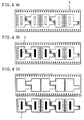
- the tape carrier 4 is manufactured in the manufacturing procedure of the tape carrier shown in Figure 4(a).
- the layout on the tape carrier 4 must be designed in such a manner that the useless areas 3 (see Figure 1(b)) are minimized, that is, as many COFs 1 as possible are manufactured out of the tape carrier 4 of a specific length. It should be appreciated, however, that the tape carrier is manufactured in the conventional manner and no additional steps are required.
- the semiconductor element 2 is bonded to a specific position of the wiring pattern formed in the manufacturing procedure of the tape carrier 4.
- the semiconductor element 2 is picked up from the semiconductor wafer and aligned to a specific position on the tape carrier 4, and heat and pressure are applied by a device called an inner lead bonder, whereby the semiconductor element 2 is bonded to the tape carrier 4.
- the wiring patterns are formed on the tape carrier 4 in different directions with respect to the direction in which the tape is fed. Accordingly, the alignment position of each semiconductor element 2 should be matched with the alignment direction of their respective wiring patterns, but only mechanism such that can rotate the picked-up semiconductor element 2 at arbitrary angles has to be provided and no further equipment is required.
- the ILB step discussed above corresponds to a first step set forth in claims below.
- the ILB step is followed by a resin applying step and an electrical testing step, and in the following punching step shown in Figure 4(C), the COFs 1 formed successively on the tape carrier 4 are punched out individually.
- This punching step is conducted by using a punching mold.
- the direction along which each COF 1 is punched out also has to be matched with the alignment direction of their respective wiring patterns, but here again, only mechanism such that can rotate the punching mold at arbitrary angles has to be provided.
- the punching step corresponds to a second step set forth in claims below.
- the COF 1 thus completed constitutes an a module structure when the external connection terminal (outlead) is connected to another circuit board in an OLB (Outer Lead Bonding) step.
- OLB Outer Lead Bonding
- the COF 1 is connected to the liquid crystal panel and the like, thereby forming a liquid crystal module.
- chip components including a resistor, a capacitor, an LED (Liquid Crystal Display), etc. can be mounted on the tape carrier 4. Consequently, the tape carrier 4 can form a module structure which also serves as a circuit board, thereby utilizing a space in the module more efficiently.
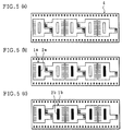
- the tape carrier manufacturing step in Figure 5(a) is identical with the step in Figure 4(a).
- more than one kind of semiconductor elements are mounted sequentially on the same tape carrier 4 by using more than one pick-up mechanism when picking up the semiconductor elements 2 from the semiconductor wafer and positioning the same to the specific positions on the tape carrier 4.
- two kinds of COFs 1a and 1b having opposite alignment directions are formed on the tape carrier 4, and accordingly, two pick-up mechanisms are provided.
- the COFs 1a and 1b form identical COFs, but at this point, the COFs having different alignment directions on the tape carrier are deemed as different kinds.
- the semiconductor element 2a is mounted on the wiring pattern which will become the COF 1a by one pick-up mechanism
- the semiconductor element 2b is mounted on the wiring pattern which will become the COF 1b by the other pick-up mechanism.
- the semiconductor elements 2a and 2b mounted on the tape carrier 4 are bonded to the same by means of heating and pressurization by the inner lead bonder.
- the positional relation between the adjacent COFs 1a and 1b is constant in the layout on the tape carrier 4. That is, when the COFs 1a (COFs 1b) alone are concerned, the alignment direction and intervals on the tape carrier 4 are constant. Hence, it is by no means difficult to mount the semiconductor element 2a onto each COF 1a by using one pick-up mechanism.
- the ILB step may be conducted with the conventional facility.
- more than one kind of semiconductor elements are mounted on the same tape carrier 4 by feeding the tape carrier 4 more than once into a bonding device composed of the pick-up mechanism and inner lead bonder.
- the step of Figure 5(b) is conducted in the first feeding
- the step of Figure 5(c) is conducted in the second feeding.
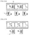
- the ILB step is followed by the resin applying step and electrical testing step. Then, in the following punching step of Figures 6(a) and 6(b), as was in the ILB step, two kinds of COFs 1 are punched out from the same tape carrier 4 with two kinds of punching molds by feeding the tape carrier 4 once into two punching devices or feeding the tape carrier 4 into one punching device twice.
- the COFs 1a are punched out by the first punching device (or in the first feeding)
- the COFs 1b are punched out by the second punching device (or in the second feeding).
- a punching mold which can simultaneously punch out two kinds of COFs 1 may be employed in the punching step.
- FIGS 7(a) through 7(c) show another embodiment of the present invention.
- a COF 11 of the present embodiment is of the shape shown in Figure 7(a), and used in the liquid crystal module.
- more than one COF is mounted at both ends of the liquid crystal panel, and in such a case, drivers each composed of mirror symmetrical COFs are mounted respectively at the top and bottom (right and left) of the liquid crystal panel.
- the arrangement of the present embodiment is particularly effective in manufacturing the mirror symmetrical COFs.
- the COFs 11a which are of the same shape as that of the COF 11 of Figure 7(a) and COFs 11b which are mirror symmetrical with respect to the COFs 11a are aligned alternately on the same tape carrier 4.
- the COFs 11b are positioned where the COFs 11a are reversed from left to right and turned by 90 degrees counter clockwise in the drawing.
- the semiconductor elements 12a are bonded to the COFs 11a, and the semiconductor elements 12b are bonded to the COFs 11b.
- the semiconductor elements 12a and 12b are rotated by 90 degrees to match with the COFs 11a and 11b on the tape carrier 4.
- two kinds of COFs 11a and 11b which are mirror symmetrical with respect to each other are aligned on the tape carrier 4 in the directions such that minimizes the useless areas of the tape carrier 4. Accordingly, more COFs can be mounted on the tape carrier 4 along its lengthwise direction, thereby utilizing the tape area efficiently.
- FIG. 7(c) shows the tape carrier on which the COFs 11a are formed in accordance with the conventional manufacturing method.
- the semiconductor elements 12a and 12b respectively bonded to the COFs 11a and 11b are not necessarily the same (that is, the semiconductor elements 12a and 12b are generally designed so as to function mirror symmetrically).
- the bonding is not conducted by merely providing mechanism which can rotate the picked-up semiconductor elements 12a and 12b at arbitrary angles as shown in Figure 4(b) in Embodiment 1.
- the semiconductor elements 12a and 12b alternately on the same tape carrier 4 by using two pick-up mechanisms, or alternatively, by feeding the tape carrier 4 twice into the bonding device composed the pick-up mechanism and inner lead bonder.
- the positional relation between the adjacent COFs 11a and 11b in the layout on the tape carrier 4 is constant. That is, when the COFs 11a (COFs 11b) alone are concerned, the alignment direction and intervals on the tape carrier 4 are constant. Hence, it is by no means difficult to mount the semiconductor element 12a onto each COF 11a by using one pick-up mechanism.
- FIG. 8 shows still another embodiment of the present invention.
- two kinds of COFs 13 and 14 of different shapes are aligned alternately on the same tape carrier 4.
- the COFs 13 and 14 are not necessarily used for the same module, and they can be used for different purposes when punched out.
- the COFs 13 and 14 are combined in such a manner that the pattern area on the tape carrier 4 can be utilized most efficiently (that is, useless areas which are not used in manufacturing the COFs are minimized).
- Figure 8 shows a case where two kinds of COFs are formed on the same tape carrier 4, but three or more kinds of COFs may be formed on the same tape carrier 4. In such a case, a plurality kinds of COFs are aligned in a specific order.
- more than one kind of COFs each having a different shape are simultaneously formed on the same tape carrier.
- this method is suitable in manufacturing the devices of many kinds with a small number of each.
- the semiconductor elements 13a and 14a bonded to the COFs 13 and 14 in the ILB step are basically of different kinds.
- the bonding is not conducted by merely providing mechanism which can rotate the picked-up semiconductor elements 13a and 14a at arbitrary angles as shown in Figure 4(b) in Embodiment 1.
- the semiconductor elements 13a and 14a alternately on the same tape carrier 4 by using two pick-up mechanisms, or alternatively, by feeding the tape carrier 4 twice into the bonding device composed the pick-up mechanism and inner lead bonder.
- the positional relation between the adjacent COFs 13 and 14 in the layout on the tape carrier 4 is constant. That is, when the COFs 13 (COFs 14) alone are concerned, the alignment direction and intervals on the tape carrier 4 are constant. Hence, it is by no means difficult to mount the semiconductor element 13a onto each COF 13 by using one pick-up mechanism.
- the positional relation between two kinds of adjacent COFs of specific kinds is constant. That is, when one specific kind of COFs alone are concerned, the alignment direction and intervals on the tape carrier 4 are constant. In other words, the COFs of the same kind are repetitively formed on the same tape carrier 4 at regular intervals.
- Embodiments 1 through 3 in the ILB step shown in Figure 2, the semiconductor element 2 and tape carrier 4 are aligned with respect to each other at the protruding electrode 9 of the former and the copper foil pattern 8 of the latter, and bonded to each other by means of heating and pressurizing by the inner lead bonder. Further, after the protruding electrode 9 is connected to the copper foil pattern 8, a space formed between the tape carrier 4 and semiconductor element 2 is filled with the sealing resin 5 to enhance moisture resistance and mechanical strength.
- the ILB step is simplified by using an anisotropic bonding agent to bond the semiconductor element and tape carrier.
- the protruding electrode 9 of the semiconductor element 2 and copper foil pattern 8 of the tape carrier 10 are bonded to each other by an anisotropic conductive bonding film 15 which is made by dispersing conductive particles 15b within an insulating bonding agent 15a.
- the anisotropic conductive bonding film 15 is transferred onto the copper foil pattern 8 of the tape carrier 10, and after the semiconductor element 2 is positioned over the same, a pressure is applied, whereby the protruding electrode 9 and copper foil pattern 8 are electrically connected through the conductive particles 15b.
- the end portion can be also sealed by the anisotropic conductive bonding film 15 as another effect.
- no sealing resin is necessary and the step of filling the space with the sealing resin can be omitted, thereby making the assembling step simpler than the one in the conventional method.
- two steps are required: bonding the protruding electrode 9 to the copper foil pattern 8 in the ILB step; and sealing the bonded portion in the resin sealing step.
- the bonding step corresponding to the ILB step can include the sealing step, thereby making the procedure simpler.
- the anisotropic conductive bonding film 15 is used as the anisotropic conductive bonding agent.
- an anisotropic conductive bonding paste 16 is used as shown in Figure 10.
- Figures 9 and 10 show the case where double-layer tape carrier 10 is used.
- the structure of the tape carrier is not especially limited, and the triple-layer tape carrier 4 can be used as well. The same can be said in Embodiments 2 and 3. In other words, in Embodiment 2 or 3, the tape carrier 4 can be replaced with the double-layer tape carrier 10.
- a tape carrier type semiconductor device of Embodiment 1 can be manufactured by:
- a tape carrier type semiconductor device of Embodiments 2 and 3 is manufactured by:
- these wiring patterns of more than one kind can be aligned in a layout such that increases a utilized area of the tape carrier by making an optimal combination.
- useless areas which have no contribution in forming the tape carrier type semiconductor devices on the tape carrier can be reduced compared with the conventional arrangement in which the wiring patterns of the same kind are aligned along the same direction.
- tape carrier type semiconductor devices of more than one kind are manufactured, these tape carrier type semiconductor devices can be manufactured simultaneously on a single kind of tape carrier.
- the arrangements of the present invention are suitable in manufacturing the devices of many kinds with a small number of each.
- the tape carrier used for the tape carrier type semiconductor device may be arranged in such a manner that the wiring patterns are fixed onto a tape carrier material forming a basis of the tape carrier through a bonding agent.
- the present invention can be applied to a triple-layer tape carrier.
- the tape carrier may be arranged in such a manner that the wiring patterns are fixed onto a tape carrier material forming a basis of the tape carrier without using any bonding agent.
- the present invention can be applied to a double-layer tape carrier.
- the above method of manufacturing a tape carrier type semiconductor device may be arranged in such a manner that each semiconductor element is rotated in accordance with an alignment direction of the wiring pattern, and then mounted on the specific position of the wiring pattern on the tape carrier.
- the semiconductor elements mounted on the wiring patterns have to be mounted in accordance with the alignment direction of the wiring patterns.
- the semiconductor elements are rotated in accordance with their respective wiring patterns and then mounted on the specific positions of the wiring patterns, thereby making it possible to mount the semiconductor elements in accordance with the alignment directions of their respective wiring patterns.
- the tape carrier type semiconductor device formed on the tape carrier may be arranged in such a manner so as to be punched out from the tape carrier by a punching mold which is allowed to rotate in accordance with an alignment direction of the wiring patterns.
- the tape carrier type semiconductor devices on the tape carrier have to be punched out in accordance with the alignment direction of the wiring patterns.
- the tape carrier type semiconductor devices on the tape carrier can be punched out in accordance with the alignment direction of the wiring patterns.
- the above manufacturing method of a tape carrier type semiconductor device may be arranged in such a manner that:
- the semiconductor elements have to be mounted on their respective wiring patterns in accordance with the kinds thereof.
- the semiconductor elements can be mounted on their respective wiring patterns in accordance with the kinds thereof.
- the wiring patterns are of the same shape, if the alignment directions are different, these wiring patterns are deemed as different kinds.
- the manufacturing method of a tape carrier type semiconductor device may be arranged in such a manner that each semiconductor element is mounted on the specific position of the wiring pattern on the tape carrier while the tape carrier is fed into a manufacturing device which conducts the bonding and mounting step as many times as the number of kinds of the wiring patterns on the tape carrier, and that the semiconductor elements to be mounted on the wiring patterns of a same kind are mounted in a same round of repetitive feeding of the tape carrier.
- the semiconductor elements can be mounted in accordance with the kinds of the wiring patterns.
- the manufacturing method of the tape carrier type semiconductor device may be arranged in such a manner that:
- the tape carrier type semiconductor devices have to be punched out from the tape carrier in accordance with the kinds (shapes) of the wiring patterns.
- the tape carrier type semiconductor devices can be punched out from the tape carrier in accordance with the kinds of the wiring patterns.
- the manufacturing method of a carrier type semiconductor device may be arranged in such a manner that:
- the tape carrier type semiconductor devices can be punched out from the wiring pattern in accordance with the kinds of the wiring patterns.
- the manufacturing method of a tape carrier type semiconductor device may be arranged in such a manner that the semiconductor element is bonded to the wiring pattern on the tape carrier by forming Au-Sn alloy.
- the gilt semiconductor electrode and the tinned wiring pattern are heated and pressurized and Au-Sn alloy is formed, whereby the semiconductor element and wiring pattern are bonded to each other.
- the conventional bonding method can be employed.
- the manufacturing method of a tape carrier type semiconductor device may be arranged in such a manner that the semiconductor element is bonded to the wiring pattern on the tape carrier by means of an anisotropic conductive bonding agent.
- the end portion can be sealed by the anisotropic conductive bonding agent as another effect.
- the sealing resin which is conventionally used to obtain the above sealing effect can be omitted.
- the sealing resin filling step can be omitted, the procedure can be simpler than the conventional procedure.
Landscapes
- Engineering & Computer Science (AREA)
- Manufacturing & Machinery (AREA)
- Microelectronics & Electronic Packaging (AREA)
- Wire Bonding (AREA)
Applications Claiming Priority (2)
| Application Number | Priority Date | Filing Date | Title |
|---|---|---|---|
| JP13452999 | 1999-05-14 | ||
| JP13452999A JP3558921B2 (ja) | 1999-05-14 | 1999-05-14 | テープキャリア並びにテープキャリア型半導体装置の製造方法 |
Publications (2)
| Publication Number | Publication Date |
|---|---|
| EP1052695A2 true EP1052695A2 (fr) | 2000-11-15 |
| EP1052695A3 EP1052695A3 (fr) | 2002-02-27 |
Family
ID=15130459
Family Applications (1)
| Application Number | Title | Priority Date | Filing Date |
|---|---|---|---|
| EP00302918A Withdrawn EP1052695A3 (fr) | 1999-05-14 | 2000-04-06 | Support à bande et methode de fabrication d'un dispositif semi-conducteur de type support à bande |
Country Status (7)
| Country | Link |
|---|---|
| US (1) | US6911729B1 (fr) |
| EP (1) | EP1052695A3 (fr) |
| JP (1) | JP3558921B2 (fr) |
| KR (1) | KR20010049250A (fr) |
| CN (1) | CN1196192C (fr) |
| SG (1) | SG98376A1 (fr) |
| TW (1) | TW595806U (fr) |
Cited By (5)
| Publication number | Priority date | Publication date | Assignee | Title |
|---|---|---|---|---|
| EP1215725A2 (fr) * | 2000-12-18 | 2002-06-19 | cubit electronics Gmbh | Assemblage utilisé pour supporter des dispositifs électriques et transpondeur sans contacts |
| US6911729B1 (en) * | 1999-05-14 | 2005-06-28 | Sharp Kabushiki Kaisha | Tape carrier semiconductor device |
| KR20050065688A (ko) * | 2003-12-23 | 2005-06-30 | 이기종 | Lcd용 cof 본딩장치 및 본딩방법 |
| CN109300879A (zh) * | 2018-09-18 | 2019-02-01 | 惠科股份有限公司 | 驱动芯片封装结构及其分离方法、分离设备 |
| CN114692547A (zh) * | 2020-12-28 | 2022-07-01 | 创意电子股份有限公司 | 集成电路芯片的接口和布置其接口的方法 |
Families Citing this family (26)
| Publication number | Priority date | Publication date | Assignee | Title |
|---|---|---|---|---|
| JP3346368B2 (ja) | 2000-02-28 | 2002-11-18 | 日本電気株式会社 | 半導体装置およびその製造方法 |
| JP2002324814A (ja) * | 2001-04-25 | 2002-11-08 | Nec Corp | Cof半導体パッケージの樹脂封止方法および装置 |
| US7173322B2 (en) * | 2002-03-13 | 2007-02-06 | Mitsui Mining & Smelting Co., Ltd. | COF flexible printed wiring board and method of producing the wiring board |
| JP3889700B2 (ja) * | 2002-03-13 | 2007-03-07 | 三井金属鉱業株式会社 | Cofフィルムキャリアテープの製造方法 |
| US20050205972A1 (en) * | 2002-03-13 | 2005-09-22 | Mitsui Mining & Smelting Co., Ltd. | COF flexible printed wiring board and semiconductor device |
| JP3829939B2 (ja) * | 2003-11-14 | 2006-10-04 | セイコーエプソン株式会社 | 半導体装置の製造方法及び製造装置 |
| KR101002346B1 (ko) * | 2003-12-30 | 2010-12-20 | 엘지디스플레이 주식회사 | 칩 실장형 필름 패키지 |
| JP4070135B2 (ja) * | 2004-05-11 | 2008-04-02 | 沖電気工業株式会社 | テープキャリア、半導体装置の製造方法および半導体装置 |
| US11842972B2 (en) * | 2004-09-28 | 2023-12-12 | Rohm Co., Ltd. | Semiconductor device with a semiconductor chip connected in a flip chip manner |
| JP4109689B2 (ja) * | 2004-09-29 | 2008-07-02 | 三井金属鉱業株式会社 | Cof用フレキシブルプリント配線板の製造方法 |
| KR101230617B1 (ko) * | 2006-06-30 | 2013-02-06 | 서울반도체 주식회사 | 발광 다이오드 및 이의 제조 방법 |
| JP4283292B2 (ja) | 2006-09-08 | 2009-06-24 | シャープ株式会社 | 半導体装置用テープキャリア、および半導体装置の製造方法 |
| KR100837281B1 (ko) * | 2007-05-23 | 2008-06-11 | 삼성전자주식회사 | 반도체 소자 패키지 및 그 제조 방법 |
| US7745260B2 (en) * | 2008-09-22 | 2010-06-29 | Freescale Semiconductor, Inc. | Method of forming semiconductor package |
| CN102237334A (zh) * | 2011-06-09 | 2011-11-09 | 深圳市华星光电技术有限公司 | Cof及cof载带 |
| US20120314175A1 (en) * | 2011-06-09 | 2012-12-13 | Shenzhen China Star Oploelectronics Technology Co., Ltd. | Cof, cof carrier tape and drive circuit of liquid crystal television |
| US20120320003A1 (en) * | 2011-06-17 | 2012-12-20 | Shenzhen China Star Optoelectronics Technology Co., Ltd. | Cof, cof carrier tape and drive circuit of liquid crystal television |
| CN102332446A (zh) * | 2011-06-17 | 2012-01-25 | 深圳市华星光电技术有限公司 | Cof及其载带 |
| CN102323682B (zh) * | 2011-08-05 | 2013-06-26 | 深圳市华星光电技术有限公司 | 液晶面板及软板上芯片构造的卷带基板 |
| US9041892B2 (en) * | 2011-08-05 | 2015-05-26 | Shenzhen China Star Optoelectronics Technology Co., Ltd. | Tape substrate for chip on film structure of liquid crystal panel |
| CN102368471B (zh) * | 2011-09-14 | 2014-04-30 | 深圳市华星光电技术有限公司 | Lcd驱动芯片的cof封装方法与结构 |
| KR101273524B1 (ko) * | 2011-10-12 | 2013-06-17 | 주식회사 루셈 | 반도체 칩 패키지 및 이를 이송하는 테이프 캐리어 패키지 |
| JP2014011046A (ja) * | 2012-06-29 | 2014-01-20 | Murata Mfg Co Ltd | 信号線路付き基材層の製造方法及び高周波信号線路の製造方法 |
| WO2019174043A1 (fr) * | 2018-03-16 | 2019-09-19 | 深圳市柔宇科技有限公司 | Support de bande cof et son procédé de traitement, et appareil de traitement de support de bande cof |
| CN110621116A (zh) * | 2019-09-25 | 2019-12-27 | 江苏上达电子有限公司 | 一种封装基板的制作方法 |
| KR20240096075A (ko) * | 2022-12-19 | 2024-06-26 | 삼성전자주식회사 | 필름 패키지 및 이를 포함하는 디스플레이 모듈 |
Family Cites Families (26)
| Publication number | Priority date | Publication date | Assignee | Title |
|---|---|---|---|---|
| US4551912A (en) | 1983-06-30 | 1985-11-12 | International Business Machines Corporation | Highly integrated universal tape bonding |
| US4977441A (en) * | 1985-12-25 | 1990-12-11 | Hitachi, Ltd. | Semiconductor device and tape carrier |
| US4811081A (en) * | 1987-03-23 | 1989-03-07 | Motorola, Inc. | Semiconductor die bonding with conductive adhesive |
| JPH0625976Y2 (ja) | 1987-04-21 | 1994-07-06 | テルモ株式会社 | 電子回路用基板接続体 |
| JPS6473628A (en) | 1987-09-14 | 1989-03-17 | Nec Corp | Tab tape |
| US5032542A (en) | 1988-11-18 | 1991-07-16 | Sanyo Electric Co., Ltd. | Method of mass-producing integrated circuit devices using strip lead frame |
| JP2751450B2 (ja) * | 1989-08-28 | 1998-05-18 | セイコーエプソン株式会社 | テープキャリアの実装構造及びその実装方法 |
| US5153707A (en) | 1989-11-06 | 1992-10-06 | Matsushita Electric Industrial Co., Ltd. | Film material for manufacturing film carriers having outer lead portions with inner and outer metallic layers |
| JP2809781B2 (ja) | 1990-01-20 | 1998-10-15 | 株式会社東芝 | インナリードボンディング装置およびインナリードボンディング方法 |
| US5075252A (en) | 1990-05-14 | 1991-12-24 | Richard Schendelman | Interdigitated trans-die lead method of construction for maximizing population density of chip-on-board construction |
| AU7954491A (en) | 1990-05-14 | 1991-12-10 | Richard Lee Schendelman | Interdigitated trans-die lead construction and method of construction for maximizing population density of chip-on-board construction |
| JPH04348540A (ja) * | 1991-05-27 | 1992-12-03 | Sony Corp | フリップチップボンダー |
| JPH0653273A (ja) | 1992-07-29 | 1994-02-25 | Nec Kansai Ltd | Tab式半導体装置とその特性検査装置 |
| JPH077043A (ja) | 1993-06-16 | 1995-01-10 | Toshiba Corp | インナ−リ−ドボンディング装置 |
| JPH07161765A (ja) | 1993-12-03 | 1995-06-23 | Hitachi Cable Ltd | フィルムキャリア型半導体装置 |
| JP3270807B2 (ja) * | 1995-06-29 | 2002-04-02 | シャープ株式会社 | テープキャリアパッケージ |
| DE19601388A1 (de) | 1996-01-16 | 1997-07-24 | Siemens Ag | Leiterplatten-Trägervorrichtung |
| US6274405B1 (en) * | 1996-10-17 | 2001-08-14 | Seiko Epson Corporation | Semiconductor device, method of making the same, circuit board, and film carrier tape |
| JP3564970B2 (ja) * | 1997-02-17 | 2004-09-15 | セイコーエプソン株式会社 | テープキャリアおよびこれを用いたテープキャリアデバイス |
| US6315156B1 (en) * | 1998-01-26 | 2001-11-13 | Gpax International, Inc. | Tape-form packaging system and apparatus for effecting assembly and disassembly thereof |
| US6100112A (en) * | 1998-05-28 | 2000-08-08 | The Furukawa Electric Co., Ltd. | Method of manufacturing a tape carrier with bump |
| JP3512655B2 (ja) * | 1998-12-01 | 2004-03-31 | シャープ株式会社 | 半導体装置およびその製造方法並びに該半導体装置の製造に使用される補強用テープ |
| JP3558921B2 (ja) * | 1999-05-14 | 2004-08-25 | シャープ株式会社 | テープキャリア並びにテープキャリア型半導体装置の製造方法 |
| JP3523536B2 (ja) * | 1999-08-06 | 2004-04-26 | シャープ株式会社 | 半導体装置及びその製造方法、並びに液晶モジュール及びその搭載方法 |
| JP3494940B2 (ja) * | 1999-12-20 | 2004-02-09 | シャープ株式会社 | テープキャリア型半導体装置、その製造方法及びそれを用いた液晶モジュール |
| JP3536023B2 (ja) * | 2000-10-13 | 2004-06-07 | シャープ株式会社 | Cof用テープキャリアおよびこれを用いて製造されるcof構造の半導体装置 |
-
1999
- 1999-05-14 JP JP13452999A patent/JP3558921B2/ja not_active Expired - Fee Related
-
2000
- 2000-03-31 US US09/540,529 patent/US6911729B1/en not_active Expired - Fee Related
- 2000-03-31 TW TW092214435U patent/TW595806U/zh unknown
- 2000-04-06 EP EP00302918A patent/EP1052695A3/fr not_active Withdrawn
- 2000-04-07 KR KR1020000018263A patent/KR20010049250A/ko not_active Ceased
- 2000-04-07 SG SG200002005A patent/SG98376A1/en unknown
- 2000-05-15 CN CNB001085689A patent/CN1196192C/zh not_active Expired - Fee Related
Cited By (5)
| Publication number | Priority date | Publication date | Assignee | Title |
|---|---|---|---|---|
| US6911729B1 (en) * | 1999-05-14 | 2005-06-28 | Sharp Kabushiki Kaisha | Tape carrier semiconductor device |
| EP1215725A2 (fr) * | 2000-12-18 | 2002-06-19 | cubit electronics Gmbh | Assemblage utilisé pour supporter des dispositifs électriques et transpondeur sans contacts |
| KR20050065688A (ko) * | 2003-12-23 | 2005-06-30 | 이기종 | Lcd용 cof 본딩장치 및 본딩방법 |
| CN109300879A (zh) * | 2018-09-18 | 2019-02-01 | 惠科股份有限公司 | 驱动芯片封装结构及其分离方法、分离设备 |
| CN114692547A (zh) * | 2020-12-28 | 2022-07-01 | 创意电子股份有限公司 | 集成电路芯片的接口和布置其接口的方法 |
Also Published As
| Publication number | Publication date |
|---|---|
| JP2000323533A (ja) | 2000-11-24 |
| KR20010049250A (ko) | 2001-06-15 |
| CN1196192C (zh) | 2005-04-06 |
| US6911729B1 (en) | 2005-06-28 |
| SG98376A1 (en) | 2003-09-19 |
| JP3558921B2 (ja) | 2004-08-25 |
| TW595806U (en) | 2004-06-21 |
| CN1274173A (zh) | 2000-11-22 |
| EP1052695A3 (fr) | 2002-02-27 |
Similar Documents
| Publication | Publication Date | Title |
|---|---|---|
| US6911729B1 (en) | Tape carrier semiconductor device | |
| KR100321883B1 (ko) | 반도체소자의실장구조및실장방법과,액정표시장치 | |
| TW563213B (en) | Semiconductor device and its manufacturing method, circuit board and electronic machine | |
| EP0653789A2 (fr) | Structure de boîtier électronique et sa fabrication | |
| US5400221A (en) | Printed circuit board mounted with electric elements thereon | |
| EP0795772B1 (fr) | Structure de connection de circuit de commande et dispositif d'affichage comportant cette structure | |
| US7109575B2 (en) | Low-cost flexible film package module and method of manufacturing the same | |
| US7087987B2 (en) | Tape circuit substrate and semiconductor chip package using the same | |
| EP0530840A1 (fr) | Module de plaque de circuit électrique et méthode pour la fabrication de module de plaque de circuit électrique | |
| EP0514723A1 (fr) | Module ayant des composants électroniques | |
| CN1113410C (zh) | 一种集成电路封装组件和组装集成电路封装的方法 | |
| US20010050431A1 (en) | Semiconductor device and liquid crystal module adopting the same | |
| JP3569025B2 (ja) | 半導体装置、およびそれを用いた電子装置 | |
| EP2086296B1 (fr) | Carte à circuit imprimé et procédé de fabrication correspondant | |
| US5444299A (en) | Electronic package with lead wire connections | |
| KR100196119B1 (ko) | 반도체장치 및 그 제조방법 및 전자 장치 | |
| KR20090106777A (ko) | 도전성 입자가 부착된 전극을 구비한 연성회로기판 및테이프 캐리어 패키지 | |
| JPH08321580A (ja) | 混成集積回路装置の構造及びその製造方法 | |
| JPH11145373A (ja) | テープキャリアパッケージおよびテープキャリアパッケージ使用の液晶表示装置 | |
| JPH04181792A (ja) | 印刷配線板の接続装置 | |
| JP3714388B2 (ja) | 半導体装置及びその製造方法、配線基板、回路基板並びに電子機器 | |
| EP0461875A2 (fr) | Dispositif de câblage | |
| JP2002124628A (ja) | 半導体装置 | |
| JPH0243596A (ja) | 平板型表示装置の電極接続構造体 | |
| JP2004177578A (ja) | 電子モジュール |
Legal Events
| Date | Code | Title | Description |
|---|---|---|---|
| PUAI | Public reference made under article 153(3) epc to a published international application that has entered the european phase |
Free format text: ORIGINAL CODE: 0009012 |
|
| AK | Designated contracting states |
Kind code of ref document: A2 Designated state(s): DE GB NL Kind code of ref document: A2 Designated state(s): AT BE CH CY DE DK ES FI FR GB GR IE IT LI LU MC NL PT SE |
|
| AX | Request for extension of the european patent |
Free format text: AL;LT;LV;MK;RO;SI |
|
| PUAL | Search report despatched |
Free format text: ORIGINAL CODE: 0009013 |
|
| AK | Designated contracting states |
Kind code of ref document: A3 Designated state(s): AT BE CH CY DE DK ES FI FR GB GR IE IT LI LU MC NL PT SE |
|
| AX | Request for extension of the european patent |
Free format text: AL;LT;LV;MK;RO;SI |
|
| RIC1 | Information provided on ipc code assigned before grant |
Free format text: 7H 01L 23/498 A, 7H 01L 21/60 B, 7H 05K 3/00 B |
|
| 17P | Request for examination filed |
Effective date: 20020416 |
|
| AKX | Designation fees paid |
Free format text: AT BE CH LI |
|
| RBV | Designated contracting states (corrected) |
Designated state(s): DE GB NL |
|
| REG | Reference to a national code |
Ref country code: DE Ref legal event code: 8566 |
|
| 17Q | First examination report despatched |
Effective date: 20050204 |
|
| 17Q | First examination report despatched |
Effective date: 20050204 |
|
| GRAP | Despatch of communication of intention to grant a patent |
Free format text: ORIGINAL CODE: EPIDOSNIGR1 |
|
| STAA | Information on the status of an ep patent application or granted ep patent |
Free format text: STATUS: THE APPLICATION IS DEEMED TO BE WITHDRAWN |
|
| 18D | Application deemed to be withdrawn |
Effective date: 20090106 |