EP1052696A2 - Elektrisches Verbindungsmedium - Google Patents
Elektrisches Verbindungsmedium Download PDFInfo
- Publication number
- EP1052696A2 EP1052696A2 EP00114951A EP00114951A EP1052696A2 EP 1052696 A2 EP1052696 A2 EP 1052696A2 EP 00114951 A EP00114951 A EP 00114951A EP 00114951 A EP00114951 A EP 00114951A EP 1052696 A2 EP1052696 A2 EP 1052696A2
- Authority
- EP
- European Patent Office
- Prior art keywords
- conductive regions
- substrate
- mesh plane
- offset
- signal path
- Prior art date
- Legal status (The legal status is an assumption and is not a legal conclusion. Google has not performed a legal analysis and makes no representation as to the accuracy of the status listed.)
- Withdrawn
Links
Images
Classifications
-
- H—ELECTRICITY
- H05—ELECTRIC TECHNIQUES NOT OTHERWISE PROVIDED FOR
- H05K—PRINTED CIRCUITS; CASINGS OR CONSTRUCTIONAL DETAILS OF ELECTRIC APPARATUS; MANUFACTURE OF ASSEMBLAGES OF ELECTRICAL COMPONENTS
- H05K1/00—Printed circuits
- H05K1/02—Details
- H05K1/0286—Programmable, customizable or modifiable circuits
- H05K1/0287—Programmable, customizable or modifiable circuits having an universal lay-out, e.g. pad or land grid patterns or mesh patterns
- H05K1/0289—Programmable, customizable or modifiable circuits having an universal lay-out, e.g. pad or land grid patterns or mesh patterns having a matrix lay-out, i.e. having selectively interconnectable sets of X-conductors and Y-conductors in different planes
-
- H—ELECTRICITY
- H10—SEMICONDUCTOR DEVICES; ELECTRIC SOLID-STATE DEVICES NOT OTHERWISE PROVIDED FOR
- H10W—GENERIC PACKAGES, INTERCONNECTIONS, CONNECTORS OR OTHER CONSTRUCTIONAL DETAILS OF DEVICES COVERED BY CLASS H10
- H10W70/00—Package substrates; Interposers; Redistribution layers [RDL]
- H10W70/60—Insulating or insulated package substrates; Interposers; Redistribution layers
- H10W70/611—Insulating or insulated package substrates; Interposers; Redistribution layers for connecting multiple chips together
-
- H—ELECTRICITY
- H10—SEMICONDUCTOR DEVICES; ELECTRIC SOLID-STATE DEVICES NOT OTHERWISE PROVIDED FOR
- H10W—GENERIC PACKAGES, INTERCONNECTIONS, CONNECTORS OR OTHER CONSTRUCTIONAL DETAILS OF DEVICES COVERED BY CLASS H10
- H10W70/00—Package substrates; Interposers; Redistribution layers [RDL]
- H10W70/60—Insulating or insulated package substrates; Interposers; Redistribution layers
- H10W70/62—Insulating or insulated package substrates; Interposers; Redistribution layers characterised by their interconnections
- H10W70/65—Shapes or dispositions of interconnections
-
- H—ELECTRICITY
- H10—SEMICONDUCTOR DEVICES; ELECTRIC SOLID-STATE DEVICES NOT OTHERWISE PROVIDED FOR
- H10W—GENERIC PACKAGES, INTERCONNECTIONS, CONNECTORS OR OTHER CONSTRUCTIONAL DETAILS OF DEVICES COVERED BY CLASS H10
- H10W70/00—Package substrates; Interposers; Redistribution layers [RDL]
- H10W70/60—Insulating or insulated package substrates; Interposers; Redistribution layers
- H10W70/67—Insulating or insulated package substrates; Interposers; Redistribution layers characterised by their insulating layers or insulating parts
- H10W70/68—Shapes or dispositions thereof
- H10W70/685—Shapes or dispositions thereof comprising multiple insulating layers
-
- H—ELECTRICITY
- H10—SEMICONDUCTOR DEVICES; ELECTRIC SOLID-STATE DEVICES NOT OTHERWISE PROVIDED FOR
- H10W—GENERIC PACKAGES, INTERCONNECTIONS, CONNECTORS OR OTHER CONSTRUCTIONAL DETAILS OF DEVICES COVERED BY CLASS H10
- H10W72/00—Interconnections or connectors in packages
- H10W72/50—Bond wires
- H10W72/531—Shapes of wire connectors
- H10W72/536—Shapes of wire connectors the connected ends being ball-shaped
-
- H—ELECTRICITY
- H10—SEMICONDUCTOR DEVICES; ELECTRIC SOLID-STATE DEVICES NOT OTHERWISE PROVIDED FOR
- H10W—GENERIC PACKAGES, INTERCONNECTIONS, CONNECTORS OR OTHER CONSTRUCTIONAL DETAILS OF DEVICES COVERED BY CLASS H10
- H10W72/00—Interconnections or connectors in packages
- H10W72/50—Bond wires
- H10W72/531—Shapes of wire connectors
- H10W72/5363—Shapes of wire connectors the connected ends being wedge-shaped
-
- H—ELECTRICITY
- H10—SEMICONDUCTOR DEVICES; ELECTRIC SOLID-STATE DEVICES NOT OTHERWISE PROVIDED FOR
- H10W—GENERIC PACKAGES, INTERCONNECTIONS, CONNECTORS OR OTHER CONSTRUCTIONAL DETAILS OF DEVICES COVERED BY CLASS H10
- H10W72/00—Interconnections or connectors in packages
- H10W72/851—Dispositions of multiple connectors or interconnections
- H10W72/874—On different surfaces
- H10W72/884—Die-attach connectors and bond wires
-
- H—ELECTRICITY
- H10—SEMICONDUCTOR DEVICES; ELECTRIC SOLID-STATE DEVICES NOT OTHERWISE PROVIDED FOR
- H10W—GENERIC PACKAGES, INTERCONNECTIONS, CONNECTORS OR OTHER CONSTRUCTIONAL DETAILS OF DEVICES COVERED BY CLASS H10
- H10W74/00—Encapsulations, e.g. protective coatings
-
- H—ELECTRICITY
- H10—SEMICONDUCTOR DEVICES; ELECTRIC SOLID-STATE DEVICES NOT OTHERWISE PROVIDED FOR
- H10W—GENERIC PACKAGES, INTERCONNECTIONS, CONNECTORS OR OTHER CONSTRUCTIONAL DETAILS OF DEVICES COVERED BY CLASS H10
- H10W90/00—Package configurations
- H10W90/701—Package configurations characterised by the relative positions of pads or connectors relative to package parts
- H10W90/731—Package configurations characterised by the relative positions of pads or connectors relative to package parts of die-attach connectors
- H10W90/734—Package configurations characterised by the relative positions of pads or connectors relative to package parts of die-attach connectors between a chip and a stacked insulating package substrate, interposer or RDL
-
- H—ELECTRICITY
- H10—SEMICONDUCTOR DEVICES; ELECTRIC SOLID-STATE DEVICES NOT OTHERWISE PROVIDED FOR
- H10W—GENERIC PACKAGES, INTERCONNECTIONS, CONNECTORS OR OTHER CONSTRUCTIONAL DETAILS OF DEVICES COVERED BY CLASS H10
- H10W90/00—Package configurations
- H10W90/701—Package configurations characterised by the relative positions of pads or connectors relative to package parts
- H10W90/751—Package configurations characterised by the relative positions of pads or connectors relative to package parts of bond wires
- H10W90/754—Package configurations characterised by the relative positions of pads or connectors relative to package parts of bond wires between a chip and a stacked insulating package substrate, interposer or RDL
-
- Y—GENERAL TAGGING OF NEW TECHNOLOGICAL DEVELOPMENTS; GENERAL TAGGING OF CROSS-SECTIONAL TECHNOLOGIES SPANNING OVER SEVERAL SECTIONS OF THE IPC; TECHNICAL SUBJECTS COVERED BY FORMER USPC CROSS-REFERENCE ART COLLECTIONS [XRACs] AND DIGESTS
- Y10—TECHNICAL SUBJECTS COVERED BY FORMER USPC
- Y10T—TECHNICAL SUBJECTS COVERED BY FORMER US CLASSIFICATION
- Y10T29/00—Metal working
- Y10T29/49—Method of mechanical manufacture
- Y10T29/49002—Electrical device making
- Y10T29/49117—Conductor or circuit manufacturing
- Y10T29/49124—On flat or curved insulated base, e.g., printed circuit, etc.
- Y10T29/49128—Assembling formed circuit to base
-
- Y—GENERAL TAGGING OF NEW TECHNOLOGICAL DEVELOPMENTS; GENERAL TAGGING OF CROSS-SECTIONAL TECHNOLOGIES SPANNING OVER SEVERAL SECTIONS OF THE IPC; TECHNICAL SUBJECTS COVERED BY FORMER USPC CROSS-REFERENCE ART COLLECTIONS [XRACs] AND DIGESTS
- Y10—TECHNICAL SUBJECTS COVERED BY FORMER USPC
- Y10T—TECHNICAL SUBJECTS COVERED BY FORMER US CLASSIFICATION
- Y10T29/00—Metal working
- Y10T29/49—Method of mechanical manufacture
- Y10T29/49002—Electrical device making
- Y10T29/49117—Conductor or circuit manufacturing
- Y10T29/49124—On flat or curved insulated base, e.g., printed circuit, etc.
- Y10T29/49155—Manufacturing circuit on or in base
- Y10T29/49156—Manufacturing circuit on or in base with selective destruction of conductive paths
-
- Y—GENERAL TAGGING OF NEW TECHNOLOGICAL DEVELOPMENTS; GENERAL TAGGING OF CROSS-SECTIONAL TECHNOLOGIES SPANNING OVER SEVERAL SECTIONS OF THE IPC; TECHNICAL SUBJECTS COVERED BY FORMER USPC CROSS-REFERENCE ART COLLECTIONS [XRACs] AND DIGESTS
- Y10—TECHNICAL SUBJECTS COVERED BY FORMER USPC
- Y10T—TECHNICAL SUBJECTS COVERED BY FORMER US CLASSIFICATION
- Y10T29/00—Metal working
- Y10T29/49—Method of mechanical manufacture
- Y10T29/49002—Electrical device making
- Y10T29/49117—Conductor or circuit manufacturing
- Y10T29/49124—On flat or curved insulated base, e.g., printed circuit, etc.
- Y10T29/49155—Manufacturing circuit on or in base
- Y10T29/49165—Manufacturing circuit on or in base by forming conductive walled aperture in base
Definitions
- the invention generally relates to integrated circuit chips and media for interconnecting same. More particularly, the invention relates to assemblies known as multichip modules (MCM) wherein unpackaged integrated circuit chips can be mounted on and wired to a substrate containing multiple patterned metal levels for power distribution and signal interconnection.
- MCM multichip modules
- An MCM generally comprises a substrate on which are formed patterned conductive regions for the interconnection of circuit components, usually integrated circuit chips.
- the conductive regions are usually made of metal and formed in multiple levels, referred to herein as metal or interconnection levels or layers.
- a substrate of an MCM can be fabricated of a variety of materials such as silicon, ceramic (for example, alumina), glass, or metal (for example, aluminum). It is also known that an interconnection level or layer can be formed on the substrate by dispositing, sputtering, evaporating, in combination sputtering and plating, or by some other technique a conductive region on a given layer. The conductive region then can be patterned into signal and power distribution conductors by photolithographic techniques combined with etching of selective plating. Multiple interconnection levels or layers can be formed so long as suitable interposing insulating layers are provided.
- Interposing levels of insulating dielectric i.e., insulating layers disposed between interconnection layers, can be applied by spinning, in the case of polymers, or chemical or physical vapor deposition, in the case of organics such as silicon dioxide. Holes (vias) patterned in these insulating layers by photolithography and wet or dry etching techniques allow interconnection from one level of metal to another.
- An MCM substrate provides an interconnection medium for a plurality of chips that is more advantageous than, for example, printed circuit boards to which are mounted individually packaged chips, because it dramatically reduces the distance required for signals to travel between chips, and thus the time delay for inter-chip signal propagation.
- this interconnection delay has become a major limitation on system performance, and thus has increased the importance of MCMs as interconnection media.
- the use of an MCM and unpackaged chips advantageously results in far greater packing density of chips, and thus reduced system size.
- MCM fabrication A disadvantage of present MCM systems of packaging and interconnection systems has been the high cost of MCM fabrication.
- the fabrication process is similar to that for integrated circuits (IC), and manufacturing equipment designed for integrated circuits generally has been used to fabricate MCMs, although an older generation of equipment generally can be used since MCM feature sizes are considerably larger than IC feature sizes.
- the manufacturing process of MCMs is essentially sequential, and the cost is roughly proportional to the number of photolithographic masks used in fabrication.
- MCM manufacturers use at least four metal or interconnection levels, and thus eight or more masks, to provide for both power distribution and signal interconnections.
- a mask is used for each level to pattern the conductive regions or conductors, and then another mask is used at each level to pattern the holes (vias) in the intervening dielectric to the next interconnection level.
- the uppermost layer of an MCM usually is a dielectric which protects the entire structure, and whose pattern of openings to underlying conductive regions allows connections to be made between chips of the MCM package and the substrate itself by means of wire bonds, solder bumps, or other interconnection means.
- top level metallization compatible with wire bond or solder interconnect processes. It is also common to include some form of capacitor dielectric for decoupling purposes between the large area power and ground planes, and this dielectric must be patterned with yet another mask. All of these mask levels contribute to fabrication complexity and cost, and each manufacturing step in some incremental manner contributes to the inevitable yield loss due to manufacturing defects.
- the combined maximum wiring density in an MCM signal plane generally can exceed 2,000 inches of wire per square inch of substrate. Yet, except in areas of the highest wiring congestion, most MCM designs use only a fraction of the available wiring capacity on the signal planes.
- a solid power distribution plane can be perforated with an array of holes with little change in the electrical characteristics thereof
- Such planes are commonly used in MCMs on layers which overlay polymer dielectrics, to allow outgassing of the polymer during curing.
- the resulting structure is known as a mesh plane.
- both power and ground potentials can be distributed on one physical layer by means of a technique referred to as interdigitation.
- interdigitation long, thin conductive regions are provided on one layer for carrying power and ground potentials or signals.
- the power and ground regions are alternatively arranged so that every other region carries power potentials or signals while the interposing regions carry a ground potential.
- parasitic inductance and resistance detrimental to noise-power-free distribution are introduced. See H. Schettler, "Passive-Silicon-Carrier Design and Characteristics", 40th Electronic Components and Technology Conference , Las Vegas, May 20-23, 1990, pp. 559-561.
- the present invention provides an interconnection medium wherein the number of interconnect layers is reduced while the low inductance power distribution characteristics of parallel power and ground planes, as well as the high wiring density for signal interconnect wires characteristic of photolithographic fabrication techniques are retained.
- the present invention inventively combines aspects of mesh planes and interdigitation to create what is referred to herein as dual offset mesh planes.
- the word “dual” denotes the provision of both power and ground planes.
- the word “offset” denotes the appearance of conductive regions of one electrical plane on two different interconnect layers.
- the invention provides an electrical interconnection medium, comprising at least first and second interconnection layers, each of the interconnection layers comprising a plurality of parallel conductive regions, the conductive regions of the second interconnection layer being oriented orthogonally to the conductive regions of the first interconnection layer, the conductive regions of the first and second interconnection layers being electrically interconnected such that at least two electrical planes are substantially interdigitated on each interconnection layer and each electrical plane appears on both interconnection layers, and such that selective conductive regions can be electrically isolated from the two electrical planes to form at least one signal path.
- the invention provides a multichip module comprising a substrate, a first interconnection layer formed on the substrate, the first interconnecting layer comprising a plurality of parallel conductive regions; an insulating layer formed on the first interconnecting layer; and a second interconnecting layer formed on the insulating layer, the second interconnecting layer comprising a plurality of parallel conductive regions that are oriented orthogonally to the conductive regions of the first interconnecting layer; the conductive regions of the first and second interconnecting layers being interconnected such that at least two distinct electrical planes are substantially interdigitated in each interconnecting layer, and each electrical plane appears on both interconnecting layers, and such that selected conductive regions can be electrically isolated from the at least two electrical planes.
- the invention provides a multichip module comprising a substrate, having an insulating top surface, first and second interconnecting layers carried on the substrate, each interconnecting layer comprising a plurality of parallel conductive regions, the conductive regions of the second interconnecting layer being oriented orthogonally to the conductive regions of the first interconnecting layer, the conductive regions of the first and second interconnecting layers being interconnected such that at least two electrical planes are provided, the electrical planes being interdigitated on each of the interconnecting layers and such that each electrical plane appears on each interconnecting layer, pads for connecting power, ground and signal conductors to electrical components, and a plurality of electrical components mounted on the pads.
- all X direction conductors are carried on a first metal layer, and all Y direction conductors are carried on a second metal layer.
- these conductive regions can be interconnected by means of a conducting hole or via through the dielectric separating the two metal layers.
- These conductive regions thus can comprise one electrical plane.
- Another plane can be incorporated into the structure by interdigitating in both metal levels a conductive region of opposite polarity between every conductor region of the first plane, and similarly connecting the overlying regions with vias to provide two offset mesh planes.
- the two metal levels can contain the electrical equivalent of two mesh planes, with the critically important topological feature that all conductive regions (i.e., conductors) lying in a given metal layer run in the same direction.
- the present invention provides a structure or medium for interconnecting semiconductor chips requiring only two metal levels. A description of the development of such a structure is described below.
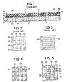
- FIG. 1 there is illustrated a section of a conventional MCM interconnection medium having four metal layers. As illustrated, formed on a substrate 10 are a ground plane layer 11, a power plane distribution layer 13 and two signal layers 15 and 17, separated by various insulating layers 12, 14 and 16.
- the substrate 10 can, for example, be made of silicon approximately 500 ⁇ m thick.
- the four metal layers 11, 13, 15 and 17 are formed on the substrate.
- a layer of silicon dioxide approximately 1 ⁇ m thick, not illustrated, is applied to the surface of the substrate 10 to insulate the first metal layer 11 from the semiconducting silicon layer 10.
- the layer 11 typically is a continuous ground plane made of sputtered aluminum approximately 2 ⁇ m thick deposited thereon.
- Separating the ground plane 11 and the power distribution plane 13 is a thin layer of silicon dioxide 12, perhaps 1 ⁇ m thick.
- This layer of silicon dioxide can be applied by chemical vapor deposition and acts as an insulator and capacitor dielectric between the power plane 13 and the ground plane 11.
- Photolithographic techniques are used to pattern holes or vias wherever connections to the ground plane are to be made. These vias typically have a diameter on the order of 500 ⁇ m and have sloping sidewalls so that subsequent metal deposition achieves good sidewall coverage and reliable connection to the ground plane 11.
- the power distribution layer 13 is applied in the same manner as the layer 11, and is likewise made of 2 ⁇ m thick aluminum. Isolated areas 25 of this power plane layer 11, which are used to make connections to the ground plane, are patterned by photolithography and wet chemical etching.
- the dielectric layer 14 can consist of a 5 ⁇ m. thick layer of silicon dioxide. Vias in this layer are used to allow connections to both the power layer 13 and the ground layer 11.
- the metal signal layer 15 is applied over the dielectric layer 14.
- Signal conductors 27 in the X direction are patterned in this layer, as are ground connection regions 24 and power connection regions 26.
- the dielectric layer 16 separates the two signal layers 15 and 17 and is patterned with many vias for making interconnections between the X and Y signal conductor segments as well as connections to the power layer 13 and ground layer 11.
- Signal vias provided in this layer 16 typically are smaller than the power vias and are approximately 10 to 20 ⁇ m in diameter.
- the metal signal layer 17 is patterned to form Y direction signal conductors as well as all of the metal pads used to make connections to the chips connected thereto, for example by means of wire bonding.
- a typical ground pad 20 is illustrated, as well as a power pad 21 and two interconnected signal pads 22 and 23.
- the MCM is completed with the application and patterning of a dielectric layer 18 which protects the underlying layers from corrosion or mechanical damage.
- the layer 18 can be approximately 10 ⁇ m thick.
- FIG. 2 there is illustrated a standard form of a mesh plane 30, which is electrically functionally equivalent to a solid plane, except for an increase in sheet resistance proportional to the percentage of metal which is not present because of the design of the mesh.
- Mesh planes of this nature generally are used on upper levels of an MCM where an intervening dielectric layer is a polymer which outgases when cured.
- Horizontal (X) conducting members 34, 35, 36 and 37 connect to vertical (Y) conducting members 30, 31, 32 and 33.
- FIG 3 there is illustrated the well-known single layer interdigitated power and ground distribution structure.
- the ground path in this structure is provided by conducting regions or conductors 41 and the power path is provided by conducting regions 42. These various conductors allow power distribution to anywhere on the module and connections to chips by way of pads included on the power and ground conductors.
- this structure has been used to build MCMs, but the electrical distribution characteristics are undesirable for general use because of the high parasitic resistance and inductance in the long, thin conductors.
- FIG 4 there is illustrated an offset mesh plane 50A , or at least a portion thereof.
- Conductive regions 50, 51, 52 and 53 typically can be of 2 ⁇ m thick and 15 ⁇ m wide and spaced on 50 ⁇ m centers. All of these dimensions are typical of those that might be advantageous on a thin film MCM. The invention has general applicability for many interconnection media and thus these dimensions are for illustrative purposes only. These conductive regions 50, 51, 52 and 53 lie on a first physical metal layer.
- Conductive regions 54, 55, 56 and 57 are of similar dimensions, but are formed on a second physical metal layer. Everywhere the conductors overlie each other, they are joined together by means of a via, such as via 58, which typically would be 10 ⁇ m in diameter through a 5 ⁇ m thick dielectric layer separating the first and second metal layers. As these vias have a low aspect ratio, they introduce very little parasitic inductance and resistance into the mesh, which otherwise is electrically equivalent to the mesh plane of Figure 2.
- the important topological difference between the mesh planes of Figure 2 and Figure 4 is that the long sections of conductors on either layer of the mesh plane of Figure 4 can be removed without destroying the overall electrical characteristics of the mesh, so long as not too many wires are removed. For example, if every other of the conductors 51, 53, 55 and 57, i.e., conductors 51 and 55, were removed, the result would still be an offset mesh plane, but with a line pitch of 100 ⁇ m instead of 50 ⁇ m. The parasitic resistance and inductance of the structure would be doubled, but the essentials of a planar distribution structure would be preserved.
- FIG 5 there is illustrated a dual offset mesh planes structure embodying features of the invention.
- distribution of both power and ground potentials by means of interdigitating respective conductors of two offset mesh planes is allowed.
- a 100 ⁇ m pitch of the conductors of the offset mesh plane of Figure 4 allows space for these interdigitated conductors.
- conductors 64 and 66 reside on a first metal layer and carry ground, while conductors 65 and 67 carry power.
- conductors 60 and 62 reside on a second metal layer and carry ground, while conductors 61 and 63 carry power.
- Vias such as 68 join ground conductors at every intersection, while vias such as via 69 join power conductors.
- the power distribution system described in connection with Figure 5 contains no provision for distributed decoupling capacitor, as described in applicant's earlier United States Patent No. 4,675,717.
- the necessary decoupling capacitance in the present system could be provided by discrete decoupling capacitors soldered or attached with conductive epoxy to interconnecting pads formed on the substrate.
- Recent advances in low inductance capacitor fabrication, such as described in the Tummala article identified above, allow this to be done in a manner which preserves a low power distribution impedance up to high frequencies.
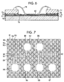
- base substrate 70 carries an unpatterned insulating layer 71 thereover. It can be appreciated that the unpatterned insulating layer 71 can be omitted if the substrate 71 itself is made of an insulating material.
- first metal layer 72 Formed over the insulating layer 71 is a first metal layer 72.
- the first metal layer 72 is patterned using the same fabrication techniques as are used in forming a conventional MCM substrate. In the view illustrated in Figure 6, conducting regions parallel to the plane of the figure are carried in the layer 72.
- a dielectric insulating layer 73 is deposited over the first metal layer 72 and is employed to separate the layer 72 from a second metal layer 74.
- the dielectric insulating layer 73 is perforated with vias such as the via 79 for the reasons set forth above.
- the second metal layer 74 also patterned, carries conductors perpendicular to the plane of Figure 6 and also includes pads such as the pad 80, used to interconnect chips, passive components, and an MC ⁇ N package or other exterior connections.
- Deposited over the layer 74 is another dielectric layer.
- the layer 75 is patterned to expose the connection pads, but otherwise protects the substrate from corrosion and mechanical damage. Layer 75 could be admitted under certain circumstances.
- the illustrated regions 76 are die attachment materials such as epoxy used to mount semiconductor dies or other components to the substrate. Regions 77 are the dies themselves. Wire bonds 78 serve to connect the bonding pads on the dies 77 to corresponding ones in the substrate.
- Figure 7 there is illustrated in plan view a dual offset mesh plane MCM. It can be appreciated that in the view illustrated in Figure 7, is revealed how conductive regions for signal interconnection in pads for interconnecting the MCM substrate to chips and to the MCM package are provided.
- the ground mesh is provided by means of X conductors such as conductor 82 in the first metal layer, Y conductors such as the conductor 80 in the second metal layer, and vias such as the via 84 at every intersection of the ground conductors.
- the power mesh is provided by means of X conductors such as the conductor 83 in the first metal layer, Y conductors such as the conductor 81 in the second metal layer, and vias such as the via 85 at every intersection of the power conductors.
- Pads are inserted into the dual offset mesh planes (i.e., formed thereon) as required for chip or external connections. To facilitate wire bonding, all pads can be 90 ⁇ m square on both metal layers, with four vias 92 in the corners thereof. A 10 ⁇ m guard band can separate the pad from the power distribution mesh.
- Isolated signal pads 88 can be used as a continuous guard band. To create a ground pad 86, all ground conductors which intersect the pad are allowed to remain.
- the power pad 87 similarly comprises only the power conductors such as conductors 81 and 83 which would intersect the pad.
- X direction signal conductors 90 in the first metal level and Y direction signal conductors 89 in the second metal level are inserted by means of a design system just as a normal router would insert wires into available wiring tracks.
- Each signal conductor segment so inserted must be surrounded by a guard band to insulate it from the power distribution mesh and must begin and end either in a via 91 to an orthogonal segment in the other metal level or at an isolated signal pad 88. All other vias which would short the signal line to portions of the power distribution system on the other metal plane would be removed by the CAD system.
- Wiring rules similar to those used by conventional CAD systems to assign wires to wiring tracks can be used to limit the density of power mesh conductors removed during the signal conductor track assignment process.
- the available signal wiring Because of the fine pitch of the wires provided by the design rules, in this example, it is possible for the available signal wiring to be substantial. If every third power distribution wire were removed, leaving power and ground pairs of wires between each pair of signal wires, and if the basic wiring pitch were 25 ⁇ m, the available signal wiring density would still be 667 inches of wire per square inch of substrate. Removing only a third of the power distribution mesh is extremely conservative, so that signal wiring densities of 1,000 wires per square inch should easily be achieved with manufacturing processes in place today.
- signal conductors formed according to the principles described above will exist in a constant impedance environment, since all mesh conductors will be at alternating current grounds and the holes in the mesh will be invisible to signals at practical frequencies of interest.
- the expected characteristic impedance of these lines will be higher than those in a strip line or a micro strip environment for the same dielectric dimensions, which is desirable so that dielectric layers can be thin.
- Cross talk should be extremely low because of the shielding characteristics of the intervening power mesh conductors between signal lines.
Landscapes
- Engineering & Computer Science (AREA)
- Microelectronics & Electronic Packaging (AREA)
- Production Of Multi-Layered Print Wiring Board (AREA)
- Structure Of Printed Boards (AREA)
- Design And Manufacture Of Integrated Circuits (AREA)
- Internal Circuitry In Semiconductor Integrated Circuit Devices (AREA)
Applications Claiming Priority (3)
| Application Number | Priority Date | Filing Date | Title |
|---|---|---|---|
| US08/024,616 US5410107A (en) | 1993-03-01 | 1993-03-01 | Multichip module |
| US24616 | 1993-03-01 | ||
| EP94102816A EP0614220B1 (de) | 1993-03-01 | 1994-02-24 | Mehrchipmodul und Herstellungsverfahren dafür |
Related Parent Applications (1)
| Application Number | Title | Priority Date | Filing Date |
|---|---|---|---|
| EP94102816A Division EP0614220B1 (de) | 1993-03-01 | 1994-02-24 | Mehrchipmodul und Herstellungsverfahren dafür |
Publications (2)
| Publication Number | Publication Date |
|---|---|
| EP1052696A2 true EP1052696A2 (de) | 2000-11-15 |
| EP1052696A3 EP1052696A3 (de) | 2001-05-02 |
Family
ID=21821522
Family Applications (2)
| Application Number | Title | Priority Date | Filing Date |
|---|---|---|---|
| EP94102816A Expired - Lifetime EP0614220B1 (de) | 1993-03-01 | 1994-02-24 | Mehrchipmodul und Herstellungsverfahren dafür |
| EP00114951A Withdrawn EP1052696A3 (de) | 1993-03-01 | 1994-02-24 | Elektrisches Verbindungsmedium |
Family Applications Before (1)
| Application Number | Title | Priority Date | Filing Date |
|---|---|---|---|
| EP94102816A Expired - Lifetime EP0614220B1 (de) | 1993-03-01 | 1994-02-24 | Mehrchipmodul und Herstellungsverfahren dafür |
Country Status (4)
| Country | Link |
|---|---|
| US (5) | US5410107A (de) |
| EP (2) | EP0614220B1 (de) |
| JP (1) | JP3138383B2 (de) |
| DE (1) | DE69430829T2 (de) |
Cited By (1)
| Publication number | Priority date | Publication date | Assignee | Title |
|---|---|---|---|---|
| DE102005012642A1 (de) * | 2005-03-18 | 2006-10-05 | Dirks, Christian, Prof. | Energiespeicher zur Stützung der Versorgungsspannung einer integrierten Schaltung |
Families Citing this family (110)
| Publication number | Priority date | Publication date | Assignee | Title |
|---|---|---|---|---|
| US5410107A (en) * | 1993-03-01 | 1995-04-25 | The Board Of Trustees Of The University Of Arkansas | Multichip module |
| JPH088393A (ja) * | 1994-06-23 | 1996-01-12 | Fujitsu Ltd | 半導体装置 |
| WO1996041376A1 (en) * | 1995-06-07 | 1996-12-19 | International Business Machines Corporation | Mesh planes for multilayer module |
| US6023408A (en) | 1996-04-09 | 2000-02-08 | The Board Of Trustees Of The University Of Arkansas | Floating plate capacitor with extremely wide band low impedance |
| US5789807A (en) * | 1996-10-15 | 1998-08-04 | International Business Machines Corporation | On-chip power distribution for improved decoupling |
| US6462976B1 (en) | 1997-02-21 | 2002-10-08 | University Of Arkansas | Conversion of electrical energy from one form to another, and its management through multichip module structures |
| US7169272B2 (en) * | 1997-04-30 | 2007-01-30 | Board Of Trustees Of The University Of Arkansas | Microfabricated recessed disk microelectrodes: characterization in static and convective solutions |
| US7144486B1 (en) | 1997-04-30 | 2006-12-05 | Board Of Trustees Of The University Of Arkansas | Multilayer microcavity devices and methods |
| US6015955A (en) * | 1997-06-20 | 2000-01-18 | International Business Machines Corporation | Reworkability solution for wirebound chips using high performance capacitor |
| US6707680B2 (en) | 1998-10-22 | 2004-03-16 | Board Of Trustees Of The University Of Arkansas | Surface applied passives |
| CA2289239C (en) * | 1998-11-23 | 2010-07-20 | Micro Coating Technologies | Formation of thin film capacitors |
| US6207522B1 (en) * | 1998-11-23 | 2001-03-27 | Microcoating Technologies | Formation of thin film capacitors |
| US6483714B1 (en) | 1999-02-24 | 2002-11-19 | Kyocera Corporation | Multilayered wiring board |
| TW430935B (en) * | 1999-03-19 | 2001-04-21 | Ind Tech Res Inst | Frame type bonding pad structure having a low parasitic capacitance |
| US6303871B1 (en) * | 1999-06-11 | 2001-10-16 | Intel Corporation | Degassing hole design for olga trace impedance |
| JP3562568B2 (ja) * | 1999-07-16 | 2004-09-08 | 日本電気株式会社 | 多層配線基板 |
| US6225687B1 (en) * | 1999-09-02 | 2001-05-01 | Intel Corporation | Chip package with degassing holes |
| KR100308872B1 (ko) * | 2000-02-23 | 2001-11-03 | 이상헌 | 다층 멀티칩 모듈 |
| JP2001284783A (ja) * | 2000-03-30 | 2001-10-12 | Shinko Electric Ind Co Ltd | 表面実装用基板及び表面実装構造 |
| US6448639B1 (en) * | 2000-09-18 | 2002-09-10 | Advanced Semiconductor Engineering, Inc. | Substrate having specific pad distribution |
| US7456028B2 (en) | 2000-10-16 | 2008-11-25 | Board Of Trustees Of The University Of Arkansas, N.A. | Electrochemical method for detecting water born pathogens |
| US7348183B2 (en) * | 2000-10-16 | 2008-03-25 | Board Of Trustees Of The University Of Arkansas | Self-contained microelectrochemical bioassay platforms and methods |
| US6887714B2 (en) | 2000-10-16 | 2005-05-03 | Board Of Trustees Of The University Of Arkansas, N.A. | Microvolume immunoabsorbant assays with amplified electrochemical detection |
| TW483293B (en) * | 2000-11-10 | 2002-04-11 | Via Tech Inc | Circuit daughter board and circuit board structure for stabilizing power source and strengthening grounding |
| US6545346B2 (en) * | 2001-03-23 | 2003-04-08 | Intel Corporation | Integrated circuit package with a capacitor |
| EP1251530A3 (de) * | 2001-04-16 | 2004-12-29 | Shipley Company LLC | Dielektrisches Laminat für einen Kondensator |
| US6459049B1 (en) * | 2001-06-20 | 2002-10-01 | Lsi Logic Corporation | High density signal routing |
| US6686819B2 (en) * | 2002-02-01 | 2004-02-03 | Intel Corporation | Dual referenced microstrip |
| US6630628B2 (en) * | 2002-02-07 | 2003-10-07 | Agilent Technologies, Inc. | High-performance laminate for integrated circuit interconnection |
| US6734472B2 (en) * | 2002-04-25 | 2004-05-11 | Synplicity, Inc. | Power and ground shield mesh to remove both capacitive and inductive signal coupling effects of routing in integrated circuit device |
| US7073154B1 (en) * | 2002-05-21 | 2006-07-04 | Altera Corporation | Apparatus and methods for interconnect zones and associated cells in integrated circuits |
| US6800939B2 (en) | 2002-05-29 | 2004-10-05 | The Board Of Trustees For The University Of Arkansas | Apparatus and method for providing low-loss transmission lines in interconnected mesh plane systems |
| US7943436B2 (en) * | 2002-07-29 | 2011-05-17 | Synopsys, Inc. | Integrated circuit devices and methods and apparatuses for designing integrated circuit devices |
| US7739624B2 (en) * | 2002-07-29 | 2010-06-15 | Synopsys, Inc. | Methods and apparatuses to generate a shielding mesh for integrated circuit devices |
| US7176383B2 (en) * | 2003-12-22 | 2007-02-13 | Endicott Interconnect Technologies, Inc. | Printed circuit board with low cross-talk noise |
| US20040226735A1 (en) * | 2003-05-12 | 2004-11-18 | Ping Wu | Method and apparatus for integrated noise decoupling |
| US20040238213A1 (en) * | 2003-05-28 | 2004-12-02 | Pitio Walter Michael | Uniform impedance printed circuit board |
| US7138716B2 (en) * | 2003-06-27 | 2006-11-21 | Intel Corporation | Addition of metal layers with signal reallocation to a microprocessor for increased frequency and lower power |
| US7096451B2 (en) * | 2003-09-09 | 2006-08-22 | International Business Machines Corporation | Mesh plane generation and file storage |
| TW594965B (en) * | 2003-09-10 | 2004-06-21 | Goyatek Technology Inc | Power supply layout structure of integrated circuit |
| US7202546B2 (en) * | 2003-10-03 | 2007-04-10 | Avago Technologies General Ip (Singapore) Pte. Ltd. | Integrated circuit with copper interconnect and top level bonding/interconnect layer |
| US20050085007A1 (en) * | 2003-10-20 | 2005-04-21 | Chuong Vu | Joining material stencil and method of use |
| US20050205292A1 (en) * | 2004-03-18 | 2005-09-22 | Etenna Corporation. | Circuit and method for broadband switching noise suppression in multilayer printed circuit boards using localized lattice structures |
| US7741696B2 (en) * | 2004-05-13 | 2010-06-22 | St-Ericsson Sa | Semiconductor integrated circuit including metal mesh structure |
| KR100655427B1 (ko) * | 2004-07-14 | 2006-12-08 | 삼성전자주식회사 | 용이하게 변경할 수 있는 배선 구조체, 상기 배선구조체의 설계 및 변경 방법 |
| US7262951B2 (en) * | 2004-09-27 | 2007-08-28 | Taiwan Semiconductor Manufacturing Co., Ltd. | De-coupling capacitors produced by utilizing dummy conductive structures integrated circuits |
| KR20080024487A (ko) * | 2005-05-31 | 2008-03-18 | 롱창 리 | 전자회로실험판 |
| US7343581B2 (en) * | 2005-06-27 | 2008-03-11 | Tela Innovations, Inc. | Methods for creating primitive constructed standard cells |
| US20070033562A1 (en) * | 2005-08-05 | 2007-02-08 | International Business Machines Corporation | Integrated circuit power distribution layout with sliding grids |
| US7335536B2 (en) * | 2005-09-01 | 2008-02-26 | Texas Instruments Incorporated | Method for fabricating low resistance, low inductance interconnections in high current semiconductor devices |
| US20070107932A1 (en) * | 2005-11-09 | 2007-05-17 | Jauniskis Linas A | Moisture resistant chip package |
| US7327030B2 (en) * | 2005-12-16 | 2008-02-05 | Atmel Corporation | Apparatus and method incorporating discrete passive components in an electronic package |
| US7590968B1 (en) | 2006-03-01 | 2009-09-15 | Tela Innovations, Inc. | Methods for risk-informed chip layout generation |
| US8658542B2 (en) | 2006-03-09 | 2014-02-25 | Tela Innovations, Inc. | Coarse grid design methods and structures |
| US9563733B2 (en) | 2009-05-06 | 2017-02-07 | Tela Innovations, Inc. | Cell circuit and layout with linear finfet structures |
| US8653857B2 (en) | 2006-03-09 | 2014-02-18 | Tela Innovations, Inc. | Circuitry and layouts for XOR and XNOR logic |
| US9230910B2 (en) | 2006-03-09 | 2016-01-05 | Tela Innovations, Inc. | Oversized contacts and vias in layout defined by linearly constrained topology |
| US7932545B2 (en) | 2006-03-09 | 2011-04-26 | Tela Innovations, Inc. | Semiconductor device and associated layouts including gate electrode level region having arrangement of six linear conductive segments with side-to-side spacing less than 360 nanometers |
| US8839175B2 (en) | 2006-03-09 | 2014-09-16 | Tela Innovations, Inc. | Scalable meta-data objects |
| US8448102B2 (en) | 2006-03-09 | 2013-05-21 | Tela Innovations, Inc. | Optimizing layout of irregular structures in regular layout context |
| US9009641B2 (en) | 2006-03-09 | 2015-04-14 | Tela Innovations, Inc. | Circuits with linear finfet structures |
| US7446352B2 (en) | 2006-03-09 | 2008-11-04 | Tela Innovations, Inc. | Dynamic array architecture |
| US8225239B2 (en) | 2006-03-09 | 2012-07-17 | Tela Innovations, Inc. | Methods for defining and utilizing sub-resolution features in linear topology |
| US7956421B2 (en) | 2008-03-13 | 2011-06-07 | Tela Innovations, Inc. | Cross-coupled transistor layouts in restricted gate level layout architecture |
| US8225261B2 (en) | 2006-03-09 | 2012-07-17 | Tela Innovations, Inc. | Methods for defining contact grid in dynamic array architecture |
| US8247846B2 (en) | 2006-03-09 | 2012-08-21 | Tela Innovations, Inc. | Oversized contacts and vias in semiconductor chip defined by linearly constrained topology |
| US7908578B2 (en) * | 2007-08-02 | 2011-03-15 | Tela Innovations, Inc. | Methods for designing semiconductor device with dynamic array section |
| US8245180B2 (en) | 2006-03-09 | 2012-08-14 | Tela Innovations, Inc. | Methods for defining and using co-optimized nanopatterns for integrated circuit design and apparatus implementing same |
| US7763534B2 (en) | 2007-10-26 | 2010-07-27 | Tela Innovations, Inc. | Methods, structures and designs for self-aligning local interconnects used in integrated circuits |
| US7943967B2 (en) | 2006-03-09 | 2011-05-17 | Tela Innovations, Inc. | Semiconductor device and associated layouts including diffusion contact placement restriction based on relation to linear conductive segments |
| US8541879B2 (en) | 2007-12-13 | 2013-09-24 | Tela Innovations, Inc. | Super-self-aligned contacts and method for making the same |
| US9035359B2 (en) | 2006-03-09 | 2015-05-19 | Tela Innovations, Inc. | Semiconductor chip including region including linear-shaped conductive structures forming gate electrodes and having electrical connection areas arranged relative to inner region between transistors of different types and associated methods |
| US7577049B1 (en) | 2006-08-08 | 2009-08-18 | Tela Innovations, Inc. | Speculative sense enable tuning apparatus and associated methods |
| US7465882B2 (en) * | 2006-12-13 | 2008-12-16 | International Business Machines Corporation | Ceramic substrate grid structure for the creation of virtual coax arrangement |
| US7979829B2 (en) * | 2007-02-20 | 2011-07-12 | Tela Innovations, Inc. | Integrated circuit cell library with cell-level process compensation technique (PCT) application and associated methods |
| US8286107B2 (en) | 2007-02-20 | 2012-10-09 | Tela Innovations, Inc. | Methods and systems for process compensation technique acceleration |
| US8667443B2 (en) | 2007-03-05 | 2014-03-04 | Tela Innovations, Inc. | Integrated circuit cell library for multiple patterning |
| JP5410664B2 (ja) * | 2007-09-04 | 2014-02-05 | 寛治 大塚 | 半導体集積回路パッケージ、プリント配線板、半導体装置および電源供給配線構造 |
| JP2009064909A (ja) * | 2007-09-05 | 2009-03-26 | Alps Electric Co Ltd | 多層セラミック配線板およびその製造方法 |
| US7834466B2 (en) * | 2007-12-17 | 2010-11-16 | Freescale Semiconductor, Inc. | Semiconductor die with die pad pattern |
| US8453094B2 (en) | 2008-01-31 | 2013-05-28 | Tela Innovations, Inc. | Enforcement of semiconductor structure regularity for localized transistors and interconnect |
| US7939443B2 (en) | 2008-03-27 | 2011-05-10 | Tela Innovations, Inc. | Methods for multi-wire routing and apparatus implementing same |
| CN201230402Y (zh) * | 2008-07-03 | 2009-04-29 | 鸿富锦精密工业(深圳)有限公司 | 印刷电路板 |
| KR101761530B1 (ko) | 2008-07-16 | 2017-07-25 | 텔라 이노베이션스, 인코포레이티드 | 동적 어레이 아키텍쳐에서의 셀 페이징과 배치를 위한 방법 및 그 구현 |
| US9122832B2 (en) | 2008-08-01 | 2015-09-01 | Tela Innovations, Inc. | Methods for controlling microloading variation in semiconductor wafer layout and fabrication |
| KR101609597B1 (ko) * | 2009-02-16 | 2016-04-07 | 삼성디스플레이 주식회사 | 회로기판 및 이를 갖는 표시패널 어셈블리 |
| US8011950B2 (en) * | 2009-02-18 | 2011-09-06 | Cinch Connectors, Inc. | Electrical connector |
| CN101902874A (zh) * | 2009-05-27 | 2010-12-01 | 鸿富锦精密工业(深圳)有限公司 | 多层印刷电路板 |
| US8247906B2 (en) * | 2009-07-06 | 2012-08-21 | Taiwan Semiconductor Manufacturing Company, Ltd. | Supplying power to integrated circuits using a grid matrix formed of through-silicon vias |
| US8288657B2 (en) * | 2009-10-12 | 2012-10-16 | International Business Machines Corporation | Noise coupling reduction and impedance discontinuity control in high-speed ceramic modules |
| US8661392B2 (en) | 2009-10-13 | 2014-02-25 | Tela Innovations, Inc. | Methods for cell boundary encroachment and layouts implementing the Same |
| US8339803B2 (en) * | 2009-12-04 | 2012-12-25 | International Business Machine Corporation | High-speed ceramic modules with hybrid referencing scheme for improved performance and reduced cost |
| US8368226B2 (en) | 2009-12-23 | 2013-02-05 | Oracle International Corporation | Die power structure |
| US8269333B2 (en) * | 2009-12-23 | 2012-09-18 | Oracle America, Inc. | Combined power mesh transition and signal overpass/underpass |
| JP5634822B2 (ja) * | 2010-10-20 | 2014-12-03 | 矢崎総業株式会社 | 電気接続箱 |
| JP5634823B2 (ja) * | 2010-10-20 | 2014-12-03 | 矢崎総業株式会社 | メタルコア基板、それを備えた電気接続箱 |
| US9159627B2 (en) | 2010-11-12 | 2015-10-13 | Tela Innovations, Inc. | Methods for linewidth modification and apparatus implementing the same |
| US8927879B2 (en) | 2010-11-22 | 2015-01-06 | International Business Machines Corporation | Crosstalk reduction between signal layers in a multilayered package by variable-width mesh plane structures |
| US8791371B2 (en) | 2011-11-28 | 2014-07-29 | International Business Machines Corporation | Mesh planes with alternating spaces for multi-layered ceramic packages |
| JP2013229470A (ja) * | 2012-04-26 | 2013-11-07 | Ps4 Luxco S A R L | 半導体装置及びそのレイアウト方法 |
| KR20150064445A (ko) * | 2013-12-03 | 2015-06-11 | 삼성전기주식회사 | 반도체 패키지용 코어리스 기판 및 그 제조 방법, 이를 이용한 반도체 패키지 제조 방법 |
| USD821337S1 (en) * | 2015-01-20 | 2018-06-26 | Modus Test Automation, Llc. | Contact field for a printed circuit board |
| USD821338S1 (en) * | 2015-01-20 | 2018-06-26 | Modus Test Automation, Llc. | Contact fields for a printed circuit board |
| CN107424974A (zh) * | 2016-05-24 | 2017-12-01 | 胡迪群 | 具有埋入式噪声屏蔽墙的封装基板 |
| JP7422542B2 (ja) * | 2016-12-15 | 2024-01-26 | サン・ディエゴ・ステート・ユニバーシティ・リサーチ・ファンデーション | 局在的配電ネットワーク設計のための重なり合わない電源/グランドプレーン |
| US11071197B2 (en) | 2018-09-21 | 2021-07-20 | International Business Machines Corporation | Multilayer ceramic electronic package with modulated mesh topology and alternating rods |
| JP2022017605A (ja) * | 2018-10-25 | 2022-01-26 | ソニーセミコンダクタソリューションズ株式会社 | 回路基板、半導体装置、および、電子機器 |
| US10825715B2 (en) | 2018-11-08 | 2020-11-03 | Silicon Space Technologies Corporation | Structures for improving radiation hardness and eliminating latch-up in integrated circuits |
| KR102601866B1 (ko) * | 2019-01-16 | 2023-11-15 | 에스케이하이닉스 주식회사 | 반도체 장치 |
| US12593738B2 (en) * | 2022-03-31 | 2026-03-31 | Texas Instruments Incorporated | Flip chip package for semiconductor devices |
Family Cites Families (33)
| Publication number | Priority date | Publication date | Assignee | Title |
|---|---|---|---|---|
| US2870400A (en) | 1955-02-11 | 1959-01-20 | Cleveland Patents Inc | Tube tester |
| US3033914A (en) | 1960-04-20 | 1962-05-08 | Gen Electric | Printed circuit boards |
| JPS5144871B2 (de) * | 1971-09-25 | 1976-12-01 | ||
| DE2611871A1 (de) | 1975-03-26 | 1976-10-07 | Honeywell Inf Systems | Elektrische schaltungsbaugruppe in mehrschichtbauweise und verfahren zu deren herstellung |
| US4330684A (en) | 1977-12-27 | 1982-05-18 | Hayward C Michael | Matrix board |
| US4522449A (en) | 1979-08-07 | 1985-06-11 | Hayward C Michael | Matrix board |
| DE2940593A1 (de) | 1979-10-06 | 1981-04-16 | Ibm Deutschland Gmbh, 7000 Stuttgart | Mehrlagen-modul mit konstantem wellenwiderstand |
| US4363930A (en) | 1980-02-04 | 1982-12-14 | Amp Incorporated | Circuit path conductors in plural planes |
| JPS6022396A (ja) * | 1983-07-19 | 1985-02-04 | 日本電気株式会社 | 回路基板 |
| US4675717A (en) * | 1984-10-09 | 1987-06-23 | American Telephone And Telegraph Company, At&T Bell Laboratories | Water-scale-integrated assembly |
| JPS61170470A (ja) * | 1985-01-18 | 1986-08-01 | 陳 森義 | 揮散速度調整可能な芳香剤等充填袋 |
| US4703288A (en) | 1985-04-03 | 1987-10-27 | American Telephone And Telegraph Company, At&T Bell Laboratories | Interconnection lines for wafer-scale-integrated assemblies |
| JPS6276544A (ja) | 1985-09-28 | 1987-04-08 | Fujitsu Ltd | 集積回路 |
| US4866507A (en) * | 1986-05-19 | 1989-09-12 | International Business Machines Corporation | Module for packaging semiconductor integrated circuit chips on a base substrate |
| JPH0716116B2 (ja) | 1986-10-24 | 1995-02-22 | 株式会社東芝 | 電子装置 |
| US4811082A (en) * | 1986-11-12 | 1989-03-07 | International Business Machines Corporation | High performance integrated circuit packaging structure |
| US4855537A (en) * | 1987-09-25 | 1989-08-08 | Kabushiki Kaisha Toshiba | Wiring substrate having mesh-shaped earth line |
| US4782193A (en) * | 1987-09-25 | 1988-11-01 | Ibm Corp. | Polygonal wiring for improved package performance |
| US5165166A (en) * | 1987-09-29 | 1992-11-24 | Microelectronics And Computer Technology Corporation | Method of making a customizable circuitry |
| US4956749A (en) * | 1987-11-20 | 1990-09-11 | Hewlett-Packard Company | Interconnect structure for integrated circuits |
| US4859806A (en) * | 1988-05-17 | 1989-08-22 | Microelectronics And Computer Technology Corporation | Discretionary interconnect |
| US4927983A (en) * | 1988-12-16 | 1990-05-22 | International Business Machines Corporation | Circuit board |
| US4899439A (en) * | 1989-06-15 | 1990-02-13 | Microelectronics And Computer Technology Corporation | Method of fabricating a high density electrical interconnect |
| US5288949A (en) * | 1992-02-03 | 1994-02-22 | Ncr Corporation | Connection system for integrated circuits which reduces cross-talk |
| JPH0770837B2 (ja) | 1992-05-20 | 1995-07-31 | インターナショナル・ビジネス・マシーンズ・コーポレイション | 多層配線を有する電子パッケージ基板及び方法 |
| US5272600A (en) * | 1992-09-02 | 1993-12-21 | Microelectronics And Computer Technology Corporation | Electrical interconnect device with interwoven power and ground lines and capacitive vias |
| US5315485A (en) | 1992-09-29 | 1994-05-24 | Mcnc | Variable size capture pads for multilayer ceramic substrates and connectors therefor |
| US5285018A (en) * | 1992-10-02 | 1994-02-08 | International Business Machines Corporation | Power and signal distribution in electronic packaging |
| CA2154156C (en) * | 1993-02-02 | 2005-04-26 | Edward D. Suski | A circuit board arrangement including shielding grids, and constructing thereof |
| US5410107A (en) * | 1993-03-01 | 1995-04-25 | The Board Of Trustees Of The University Of Arkansas | Multichip module |
| US5585602A (en) | 1995-01-09 | 1996-12-17 | Massachusetts Institute Of Technology | Structure for providing conductive paths |
| JP3113153B2 (ja) | 1994-07-26 | 2000-11-27 | 株式会社東芝 | 多層配線構造の半導体装置 |
| US5764489A (en) | 1996-07-18 | 1998-06-09 | Compaq Computer Corporation | Apparatus for controlling the impedance of high speed signals on a printed circuit board |
-
1993
- 1993-03-01 US US08/024,616 patent/US5410107A/en not_active Expired - Lifetime
-
1994
- 1994-02-24 EP EP94102816A patent/EP0614220B1/de not_active Expired - Lifetime
- 1994-02-24 EP EP00114951A patent/EP1052696A3/de not_active Withdrawn
- 1994-02-24 DE DE69430829T patent/DE69430829T2/de not_active Expired - Fee Related
- 1994-03-01 JP JP06054935A patent/JP3138383B2/ja not_active Expired - Fee Related
-
1995
- 1995-02-28 US US08/396,447 patent/US6297460B1/en not_active Expired - Fee Related
-
1997
- 1997-09-05 US US08/924,097 patent/US6255600B1/en not_active Expired - Fee Related
-
2001
- 2001-04-25 US US09/841,601 patent/US6388200B2/en not_active Expired - Fee Related
- 2001-06-22 US US09/885,981 patent/US20010047588A1/en not_active Abandoned
Cited By (1)
| Publication number | Priority date | Publication date | Assignee | Title |
|---|---|---|---|---|
| DE102005012642A1 (de) * | 2005-03-18 | 2006-10-05 | Dirks, Christian, Prof. | Energiespeicher zur Stützung der Versorgungsspannung einer integrierten Schaltung |
Also Published As
| Publication number | Publication date |
|---|---|
| US6388200B2 (en) | 2002-05-14 |
| EP0614220A3 (de) | 1995-03-01 |
| EP1052696A3 (de) | 2001-05-02 |
| JPH0794666A (ja) | 1995-04-07 |
| US20010047588A1 (en) | 2001-12-06 |
| US6297460B1 (en) | 2001-10-02 |
| US5410107A (en) | 1995-04-25 |
| EP0614220A2 (de) | 1994-09-07 |
| DE69430829D1 (de) | 2002-07-25 |
| DE69430829T2 (de) | 2002-10-10 |
| US20010013422A1 (en) | 2001-08-16 |
| EP0614220B1 (de) | 2002-06-19 |
| US6255600B1 (en) | 2001-07-03 |
| JP3138383B2 (ja) | 2001-02-26 |
Similar Documents
| Publication | Publication Date | Title |
|---|---|---|
| US5410107A (en) | Multichip module | |
| US5272600A (en) | Electrical interconnect device with interwoven power and ground lines and capacitive vias | |
| US5770476A (en) | Passive interposer including at least one passive electronic component | |
| US5935687A (en) | Three dimensional package and architecture for high performance computer | |
| KR100611267B1 (ko) | 인터포저를 구비한 고성능, 저비용 마이크로일렉트로닉회로 패키지 | |
| US6242279B1 (en) | High density wire bond BGA | |
| CN100355064C (zh) | 低成本微电子电路封装 | |
| US20230420494A1 (en) | Deep trench capacitors embedded in package substrate | |
| US7535109B2 (en) | Die assembly having electrical interconnect | |
| EP0070380B1 (de) | Diskreter Dünnschichtkondensator | |
| US7271031B2 (en) | Universal interconnect die | |
| WO1992003844A1 (en) | Multilayer integrated circuit module | |
| JP3899059B2 (ja) | 低抵抗高密度信号線をする電子パッケージおよびその製造方法 | |
| KR100550298B1 (ko) | 병렬 평면 기판 | |
| US5541814A (en) | Personalizable multi-chip carrier including removable fuses | |
| US6177732B1 (en) | Multi-layer organic land grid array to minimize via inductance | |
| US20020048927A1 (en) | Embedded capacitor multi-chip modules | |
| US10453787B2 (en) | Method and apparatus for forming multi-layered vias in sequentially fabricated circuits | |
| US20070176287A1 (en) | Thin integrated circuit device packages for improved radio frequency performance | |
| Schaper | Multichip module and method of forming same | |
| JPS61168936A (ja) | 配線 |
Legal Events
| Date | Code | Title | Description |
|---|---|---|---|
| PUAI | Public reference made under article 153(3) epc to a published international application that has entered the european phase |
Free format text: ORIGINAL CODE: 0009012 |
|
| 17P | Request for examination filed |
Effective date: 20000719 |
|
| AC | Divisional application: reference to earlier application |
Ref document number: 614220 Country of ref document: EP |
|
| AK | Designated contracting states |
Kind code of ref document: A2 Designated state(s): DE FR GB |
|
| PUAL | Search report despatched |
Free format text: ORIGINAL CODE: 0009013 |
|
| AK | Designated contracting states |
Kind code of ref document: A3 Designated state(s): DE FR GB |
|
| RIN1 | Information on inventor provided before grant (corrected) |
Inventor name: SCHAPER, LEONARD W. |
|
| AKX | Designation fees paid |
Free format text: DE FR GB |
|
| 17Q | First examination report despatched |
Effective date: 20020226 |
|
| STAA | Information on the status of an ep patent application or granted ep patent |
Free format text: STATUS: THE APPLICATION IS DEEMED TO BE WITHDRAWN |
|
| 18D | Application deemed to be withdrawn |
Effective date: 20040129 |