EP1065711A2 - Verfahren zur Herstellung eines plattierten elektronischen Leiteranschluss - Google Patents
Verfahren zur Herstellung eines plattierten elektronischen Leiteranschluss Download PDFInfo
- Publication number
- EP1065711A2 EP1065711A2 EP00109592A EP00109592A EP1065711A2 EP 1065711 A2 EP1065711 A2 EP 1065711A2 EP 00109592 A EP00109592 A EP 00109592A EP 00109592 A EP00109592 A EP 00109592A EP 1065711 A2 EP1065711 A2 EP 1065711A2
- Authority
- EP
- European Patent Office
- Prior art keywords
- coating
- lead
- manufacturing
- metal leads
- leads
- Prior art date
- Legal status (The legal status is an assumption and is not a legal conclusion. Google has not performed a legal analysis and makes no representation as to the accuracy of the status listed.)
- Withdrawn
Links
Images


Classifications
-
- H—ELECTRICITY
- H10—SEMICONDUCTOR DEVICES; ELECTRIC SOLID-STATE DEVICES NOT OTHERWISE PROVIDED FOR
- H10W—GENERIC PACKAGES, INTERCONNECTIONS, CONNECTORS OR OTHER CONSTRUCTIONAL DETAILS OF DEVICES COVERED BY CLASS H10
- H10W70/00—Package substrates; Interposers; Redistribution layers [RDL]
- H10W70/40—Leadframes
- H10W70/456—Materials
- H10W70/457—Materials of metallic layers on leadframes
-
- H—ELECTRICITY
- H10—SEMICONDUCTOR DEVICES; ELECTRIC SOLID-STATE DEVICES NOT OTHERWISE PROVIDED FOR
- H10W—GENERIC PACKAGES, INTERCONNECTIONS, CONNECTORS OR OTHER CONSTRUCTIONAL DETAILS OF DEVICES COVERED BY CLASS H10
- H10W72/00—Interconnections or connectors in packages
-
- H—ELECTRICITY
- H10—SEMICONDUCTOR DEVICES; ELECTRIC SOLID-STATE DEVICES NOT OTHERWISE PROVIDED FOR
- H10W—GENERIC PACKAGES, INTERCONNECTIONS, CONNECTORS OR OTHER CONSTRUCTIONAL DETAILS OF DEVICES COVERED BY CLASS H10
- H10W70/00—Package substrates; Interposers; Redistribution layers [RDL]
- H10W70/01—Manufacture or treatment
- H10W70/04—Manufacture or treatment of leadframes
- H10W70/048—Mechanical treatments, e.g. punching, cutting, deforming or cold welding
-
- H—ELECTRICITY
- H10—SEMICONDUCTOR DEVICES; ELECTRIC SOLID-STATE DEVICES NOT OTHERWISE PROVIDED FOR
- H10W—GENERIC PACKAGES, INTERCONNECTIONS, CONNECTORS OR OTHER CONSTRUCTIONAL DETAILS OF DEVICES COVERED BY CLASS H10
- H10W72/00—Interconnections or connectors in packages
- H10W72/01—Manufacture or treatment
- H10W72/0198—Manufacture or treatment batch processes
-
- H—ELECTRICITY
- H10—SEMICONDUCTOR DEVICES; ELECTRIC SOLID-STATE DEVICES NOT OTHERWISE PROVIDED FOR
- H10W—GENERIC PACKAGES, INTERCONNECTIONS, CONNECTORS OR OTHER CONSTRUCTIONAL DETAILS OF DEVICES COVERED BY CLASS H10
- H10W72/00—Interconnections or connectors in packages
- H10W72/071—Connecting or disconnecting
- H10W72/075—Connecting or disconnecting of bond wires
-
- H—ELECTRICITY
- H10—SEMICONDUCTOR DEVICES; ELECTRIC SOLID-STATE DEVICES NOT OTHERWISE PROVIDED FOR
- H10W—GENERIC PACKAGES, INTERCONNECTIONS, CONNECTORS OR OTHER CONSTRUCTIONAL DETAILS OF DEVICES COVERED BY CLASS H10
- H10W72/00—Interconnections or connectors in packages
- H10W72/90—Bond pads, in general
- H10W72/951—Materials of bond pads
- H10W72/952—Materials of bond pads comprising metals or metalloids, e.g. PbSn, Ag or Cu
-
- H—ELECTRICITY
- H10—SEMICONDUCTOR DEVICES; ELECTRIC SOLID-STATE DEVICES NOT OTHERWISE PROVIDED FOR
- H10W—GENERIC PACKAGES, INTERCONNECTIONS, CONNECTORS OR OTHER CONSTRUCTIONAL DETAILS OF DEVICES COVERED BY CLASS H10
- H10W74/00—Encapsulations, e.g. protective coatings
-
- H—ELECTRICITY
- H10—SEMICONDUCTOR DEVICES; ELECTRIC SOLID-STATE DEVICES NOT OTHERWISE PROVIDED FOR
- H10W—GENERIC PACKAGES, INTERCONNECTIONS, CONNECTORS OR OTHER CONSTRUCTIONAL DETAILS OF DEVICES COVERED BY CLASS H10
- H10W90/00—Package configurations
- H10W90/701—Package configurations characterised by the relative positions of pads or connectors relative to package parts
- H10W90/751—Package configurations characterised by the relative positions of pads or connectors relative to package parts of bond wires
- H10W90/756—Package configurations characterised by the relative positions of pads or connectors relative to package parts of bond wires between a chip and a stacked lead frame, conducting package substrate or heat sink
-
- Y—GENERAL TAGGING OF NEW TECHNOLOGICAL DEVELOPMENTS; GENERAL TAGGING OF CROSS-SECTIONAL TECHNOLOGIES SPANNING OVER SEVERAL SECTIONS OF THE IPC; TECHNICAL SUBJECTS COVERED BY FORMER USPC CROSS-REFERENCE ART COLLECTIONS [XRACs] AND DIGESTS
- Y10—TECHNICAL SUBJECTS COVERED BY FORMER USPC
- Y10T—TECHNICAL SUBJECTS COVERED BY FORMER US CLASSIFICATION
- Y10T29/00—Metal working
- Y10T29/49—Method of mechanical manufacture
- Y10T29/49002—Electrical device making
- Y10T29/49117—Conductor or circuit manufacturing
- Y10T29/49121—Beam lead frame or beam lead device
-
- Y—GENERAL TAGGING OF NEW TECHNOLOGICAL DEVELOPMENTS; GENERAL TAGGING OF CROSS-SECTIONAL TECHNOLOGIES SPANNING OVER SEVERAL SECTIONS OF THE IPC; TECHNICAL SUBJECTS COVERED BY FORMER USPC CROSS-REFERENCE ART COLLECTIONS [XRACs] AND DIGESTS
- Y10—TECHNICAL SUBJECTS COVERED BY FORMER USPC
- Y10T—TECHNICAL SUBJECTS COVERED BY FORMER US CLASSIFICATION
- Y10T29/00—Metal working
- Y10T29/49—Method of mechanical manufacture
- Y10T29/49002—Electrical device making
- Y10T29/49117—Conductor or circuit manufacturing
- Y10T29/49204—Contact or terminal manufacturing
-
- Y—GENERAL TAGGING OF NEW TECHNOLOGICAL DEVELOPMENTS; GENERAL TAGGING OF CROSS-SECTIONAL TECHNOLOGIES SPANNING OVER SEVERAL SECTIONS OF THE IPC; TECHNICAL SUBJECTS COVERED BY FORMER USPC CROSS-REFERENCE ART COLLECTIONS [XRACs] AND DIGESTS
- Y10—TECHNICAL SUBJECTS COVERED BY FORMER USPC
- Y10T—TECHNICAL SUBJECTS COVERED BY FORMER US CLASSIFICATION
- Y10T29/00—Metal working
- Y10T29/49—Method of mechanical manufacture
- Y10T29/49002—Electrical device making
- Y10T29/49117—Conductor or circuit manufacturing
- Y10T29/49204—Contact or terminal manufacturing
- Y10T29/49208—Contact or terminal manufacturing by assembling plural parts
- Y10T29/4921—Contact or terminal manufacturing by assembling plural parts with bonding
- Y10T29/49211—Contact or terminal manufacturing by assembling plural parts with bonding of fused material
-
- Y—GENERAL TAGGING OF NEW TECHNOLOGICAL DEVELOPMENTS; GENERAL TAGGING OF CROSS-SECTIONAL TECHNOLOGIES SPANNING OVER SEVERAL SECTIONS OF THE IPC; TECHNICAL SUBJECTS COVERED BY FORMER USPC CROSS-REFERENCE ART COLLECTIONS [XRACs] AND DIGESTS
- Y10—TECHNICAL SUBJECTS COVERED BY FORMER USPC
- Y10T—TECHNICAL SUBJECTS COVERED BY FORMER US CLASSIFICATION
- Y10T29/00—Metal working
- Y10T29/49—Method of mechanical manufacture
- Y10T29/49002—Electrical device making
- Y10T29/49117—Conductor or circuit manufacturing
- Y10T29/49204—Contact or terminal manufacturing
- Y10T29/49208—Contact or terminal manufacturing by assembling plural parts
- Y10T29/49218—Contact or terminal manufacturing by assembling plural parts with deforming
-
- Y—GENERAL TAGGING OF NEW TECHNOLOGICAL DEVELOPMENTS; GENERAL TAGGING OF CROSS-SECTIONAL TECHNOLOGIES SPANNING OVER SEVERAL SECTIONS OF THE IPC; TECHNICAL SUBJECTS COVERED BY FORMER USPC CROSS-REFERENCE ART COLLECTIONS [XRACs] AND DIGESTS
- Y10—TECHNICAL SUBJECTS COVERED BY FORMER USPC
- Y10T—TECHNICAL SUBJECTS COVERED BY FORMER US CLASSIFICATION
- Y10T29/00—Metal working
- Y10T29/49—Method of mechanical manufacture
- Y10T29/49002—Electrical device making
- Y10T29/49117—Conductor or circuit manufacturing
- Y10T29/49204—Contact or terminal manufacturing
- Y10T29/49224—Contact or terminal manufacturing with coating
Definitions
- a lead is the metal wiring protruding from the integrated circuit package which is used to create an electrical connection with the circuit board upon which the integrated circuit will be mounted.
- a termination is a surface that is used to create an electrical connection between any electrical or electronic elements.
- a connection is deemed satisfactory when it meets industry defined requirements of visual properties of wetting and filleting and furnishes a path that does not alter the intended electrical characteristics of signals that are transmitted through it. Wetting is the ability of a liquid to spread over or cover over a solid surface with which it makes contact. Filleting is a description of the volume, height, area and circumference of a joining material used to connect two surfaces. The connection must also be mechanically permanent.
- soldering In soldering, two metal surfaces are united when a solder junction is formed between them.
- Solder is a metal or metal composition which melts at a fairly low temperature (approximately 200 C) and wets the surfaces to which it is applied in the molten state.
- Solder is an alloy, such as zinc and copper, or tin and lead. Upon cooling, solder forms a permanent mechanical and electrical connection between the surface of the semiconductor lead/ termination and the surface of the circuit board.
- solderability is the ability of a material or surface to be wetted with molten solder under specified conditions.
- the manufacturing processing of making a packaged IC includes the application of a lead/termination finish to the metal leads/terminations to preserve and enhance the inherent solderability of the underlying basis metal leads/terminations.
- This lead/termination finish is typically applied as a thin coating.
- the lead/termination finish preserves the metal leads/ terminations and allows the packaged IC or electrical/electronic component to be readily soldered into the circuit board.
- the present invention includes a method of manufacturing a lead or termination of electrical devices comprising the steps of applying a coating to the metal leads/terminations, flattening the metal leads/ terminations until the coated lead is substantially smoother and substantially less porous, and substantially flattening until there is a reduction of about .1% to about 10% in coating thickness.
- the invention also includes a method of manufacturing a metal lead of an integrated circuit comprising the steps of applying a coating to the metal leads of the integrated circuit package, flattening the metal leads until the coated lead is substantially smoother and substantially less porous, applying the coating to the metal leads/terminations so that the coating has a thickness of about 10 microinches to about 1000 microinches prior to flattening and there is a reduction of about .1% to about 10% in coating thickness after flattening and flattening until there is a reduction of about 80% to 90% in the porosity of the coating.
- hot dip processes provide a high quality finish, but controlling the coating thickness distribution is difficult.
- the maximum coating thickness attained is limited due to liquid surface tension considerations.
- Plating processes are much more easily controlled with respect to coating thickness distribution.
- the maximum coating thickness achievable is unbounded.
- the solderability, or the ability of a surface to be wetted by molten solder, of plating is typically not as good as molten hot dip lead/terminations finishes.
- the present invention is an method of manufacturing IC packaging so that the leads have a higher degree of solderability. This improvement has been measured and tested using steam aging and wetting balance measurements.
- the method of making a lead finish incorporates mechanically flattening the plated coating of the leads.
- This may be accomplished by mechanical means such as rolling, stamping, peening (surface-hardening a piece of metal by hammering or bombarding with a hard shot), coining (forming metals by squeezing between two dies so as to impress well-defined imprints on both surfaces of the work), forging (using compressive force to shape metal by plastic deformation) or other suitable flattening techniques.
- rolling produces superior results.
- stamping peening
- peening surface-hardening a piece of metal by hammering or bombarding with a hard shot
- coining forming metals by squeezing between two dies so as to impress well-defined imprints on both surfaces of the work
- forging using compressive force to shape metal by plastic deformation
- Flattening the lead of an electronic device increases the solderability of the lead. Flattening may be accomplished by rolling, stamping, peening, coining, or forging.
- Packaged integrated circuits are manufactured using metal lead frames that have substantially flat surfaces.
- the integrated circuit in chip (die) form is attached to the lead frame (which may have a special silver or copper spot plated on it for die attachment), wire bonded and either transfer molded, furnace sealed or welded to produce an encapsulated (packaged) integrated circuit with leads protruding from the package body.
- Figure 1 shows the outline of a ribbon 10 containing a metal lead frame 11 which includes a central die pad 12 and a plurality of leads 14.
- the IC chips (not shown) are mounted on die pads 12.
- the integrated circuits chips are spaced interstitially and mounted upon IC die pads 12 which conform substantially to the shape of the be chip attached (e.g., rectangular as shown).
- Flat metal leads 14 make an electrical contact with the bond pads of the integrated circuit with thin bond wires (not shown) extending from the lead to a bond pad on the IC.
- the metal leads 14 As seen in Fig. 1, at the inner end 16 of the metal leads 14 surround the circumference of the IC die pad 12. The metal leads 14 all extend radially outward from the IC die pad 12. At the outer end 18 of the metal leads 14, the metal leads 14 project at an angle parallel with the ribbon 10 towards the metal leads 14 of the next IC packaging frame.
- Adjacent leads are held together and are held on the frame by dam bars 30.
- the die pad 12 is connected to rails 34 by the tie bars 32.
- the lead frame is placed in the mold. Molten plastic is transfer molded into the mold to enclose the die and the leads inside the perimeter formed by the rails 34 and damn bars 30.
- the dam bars 30 and the tie bars 32 are severed from the rails 34 in a conventional lead trim operation.
- the leads 14 may then be bent to a desired angle in a conventional forming operation. This results in frames for individual IC packages.
- the coaling of the metal leads 14 are flattened. This may be accomplished by mechanical means such as rolling, stamping, peening, coining, forging or other suitable flattening techniques.
- the bent metal leads 14 are inserted in and soldered to the circuit board.
- the coating on the leads have a thickness of about 10 microinches to about 1000 microinches, with the solderability surface contact area representing about 10-100 % of the total surface area of the coating.
- the lead thickness is reduced from .1% to about 10% of its original size prior to flattening.
- Figs. 2-4 are photo micrographs of the coated surface of the leads. At the bottom far left is the serial number of the picture, which the reader may ignore. The second number, 2 KV, represents the voltage applied to the electronic microscope.
- Figs. 2(a), 3(a), and 4(a) show the coated lead surface 20 magnified 3,000 times.
- Figs. 2(b), 3(b), and 4(b), and 5(b) show the coated lead surface 20 magnified 500 times.
- Figs. 2(a) and 2(b) shows a lead coating that was flattened on the left hand side but not flattened on the right. The difference in smoothness in Figs.
- Figs. 2(a) and 2(a) should be contrasted with Figs. 3(a) and Fig. 3(b), the later two being un-flattened. Note however how substantially smoother the partially flattened surface of 2(a) as compared to the un-flattened surface of 3(a). The same is also true comparing the partially flattened section of Fig. 2(b) with un-flattened surface shown in Fig. 3(b).
- Figs. 4(a) and 4(b) show the result of hammering. Comparing Figs. 4(a) and 4(b) to 3(a) and 3(b) reveals that hammering smooths the surface and reduces porosity. Note the rougher sections 200 that were missed by the hammer.
- the lead coating in this specific embodiment comprises consist of 80/20 Tin/Lead. These leads are used for devices packaged in the Harris TO-220 package.
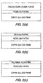
- Figs. 5(a), 5(b) and 5(c) shows varying lead frames and their coatings.
- Figs. 5(a), 5(b) and 5(c) all show a lead frame bottom layer of copper and a middle layer of nickel plating.
- the top layer of plating (which provides the solderability surface contact area) differs for each-in 5(a) the top layer plating is of tin/lead solder plating, in 5(b) the top layer is of gold plating, in 5(c) the top layer is of palladium plating.
- Using a coating of gold on nickel whereby the coating of gold is 2 micro-inches or less is a preferred embodiment. Using any of these aforementioned combinations is contemplated.
- a method of making a lead finish incorporating mechanically flattening the plated coating of metal leads This may be accomplished by mechanical means such as rolling, stamping, peening, coining, forging.
Landscapes
- Lead Frames For Integrated Circuits (AREA)
- Connections Effected By Soldering, Adhesion, Or Permanent Deformation (AREA)
- Shaping Metal By Deep-Drawing, Or The Like (AREA)
- Electroplating Methods And Accessories (AREA)
- Coating With Molten Metal (AREA)
- Other Surface Treatments For Metallic Materials (AREA)
- Wire Bonding (AREA)
Applications Claiming Priority (2)
| Application Number | Priority Date | Filing Date | Title |
|---|---|---|---|
| US343845 | 1999-06-30 | ||
| US09/343,845 US7174626B2 (en) | 1999-06-30 | 1999-06-30 | Method of manufacturing a plated electronic termination |
Publications (2)
| Publication Number | Publication Date |
|---|---|
| EP1065711A2 true EP1065711A2 (de) | 2001-01-03 |
| EP1065711A3 EP1065711A3 (de) | 2001-11-07 |
Family
ID=23347929
Family Applications (1)
| Application Number | Title | Priority Date | Filing Date |
|---|---|---|---|
| EP00109592A Withdrawn EP1065711A3 (de) | 1999-06-30 | 2000-05-05 | Verfahren zur Herstellung eines plattierten elektronischen Leiteranschluss |
Country Status (5)
| Country | Link |
|---|---|
| US (1) | US7174626B2 (de) |
| EP (1) | EP1065711A3 (de) |
| JP (1) | JP2001060649A (de) |
| KR (1) | KR20010049673A (de) |
| TW (1) | TW469544B (de) |
Cited By (2)
| Publication number | Priority date | Publication date | Assignee | Title |
|---|---|---|---|---|
| US7174626B2 (en) * | 1999-06-30 | 2007-02-13 | Intersil Americas, Inc. | Method of manufacturing a plated electronic termination |
| EP4312250A1 (de) * | 2022-07-28 | 2024-01-31 | STMicroelectronics S.r.l. | Verfahren zur herstellung von halbleiterbauelementen, entsprechendes substrat und halbleiterbauelement |
Families Citing this family (5)
| Publication number | Priority date | Publication date | Assignee | Title |
|---|---|---|---|---|
| CN1299547C (zh) * | 2000-07-12 | 2007-02-07 | 罗姆股份有限公司 | 导体间的连接结构及其连接方法 |
| US7309909B2 (en) * | 2005-09-21 | 2007-12-18 | Texas Instruments Incorporated | Leadframes for improved moisture reliability of semiconductor devices |
| CN101295695A (zh) * | 2007-04-29 | 2008-10-29 | 飞思卡尔半导体(中国)有限公司 | 具有焊料流动控制的引线框架 |
| JP5079605B2 (ja) * | 2008-06-30 | 2012-11-21 | 株式会社オートネットワーク技術研究所 | 圧着端子及び端子付電線並びにこれらの製造方法 |
| DE102018213639A1 (de) * | 2018-08-14 | 2020-02-20 | Te Connectivity Germany Gmbh | Verfahren zum Anbringen wenigstens eines insbesondere stiftförmigen Kontaktelements auf einer Leiterbahn einer Leiterplatte, Stiftleiste zur Anbringung auf einer Leiterplatte, Verbindungsanordnung |
Family Cites Families (36)
| Publication number | Priority date | Publication date | Assignee | Title |
|---|---|---|---|---|
| DE2444892C3 (de) * | 1974-09-19 | 1982-03-18 | Siemens AG, 1000 Berlin und 8000 München | Verfahren zur Herstellung von streifenförmigen Anschlußelementen |
| US4055062A (en) | 1975-07-15 | 1977-10-25 | Allegheny Ludlum Industries, Inc. | Process for manufacturing strip lead frames |
| US4089733A (en) * | 1975-09-12 | 1978-05-16 | Amp Incorporated | Method of forming complex shaped metal-plastic composite lead frames for IC packaging |
| US4214120A (en) * | 1978-10-27 | 1980-07-22 | Western Electric Company, Inc. | Electronic device package having solder leads and methods of assembling the package |
| JPS57133655A (en) * | 1981-02-10 | 1982-08-18 | Pioneer Electronic Corp | Lead frame |
| JPS59172253A (ja) * | 1983-03-18 | 1984-09-28 | Mitsubishi Electric Corp | 半導体装置 |
| JPS60225455A (ja) | 1984-04-24 | 1985-11-09 | Kobe Steel Ltd | リ−ドフレ−ム |
| JPS6148951A (ja) | 1984-08-16 | 1986-03-10 | Toshiba Corp | 半導体装置 |
| JPS61234554A (ja) | 1985-04-11 | 1986-10-18 | Mitsubishi Electric Corp | 半導体用リ−ドフレ−ムの製造方法 |
| JPS6372895A (ja) | 1986-09-17 | 1988-04-02 | Nippon Mining Co Ltd | 電子・電気機器用部品の製造方法 |
| JPS63306648A (ja) | 1987-06-08 | 1988-12-14 | Shinko Electric Ind Co Ltd | 半導体装置用リ−ドフレ−ムとその製造方法 |
| US5059455A (en) * | 1988-03-08 | 1991-10-22 | Cyclops Corporation | Method for galvanizing perforated steel sheet |
| US5258331A (en) * | 1989-10-20 | 1993-11-02 | Texas Instruments Incorporated | Method of manufacturing resin-encapsulated semiconductor device package using photoresist or pre-peg lead frame dam bars |
| JPH03230556A (ja) * | 1990-02-06 | 1991-10-14 | Matsushita Electron Corp | 半導体装置用リードフレーム |
| JP2580059B2 (ja) * | 1990-03-23 | 1997-02-12 | シャープ株式会社 | 固体撮像素子およびその製造方法 |
| US5235743A (en) * | 1990-07-11 | 1993-08-17 | Yazaki Corporation | Method of manufacturing a pair of terminals having a low friction material on a mating surface to facilitate connection of the terminals |
| JPH04268055A (ja) * | 1991-02-22 | 1992-09-24 | Yamaha Corp | リードフレーム用銅合金の製造方法 |
| US5151846A (en) * | 1991-08-23 | 1992-09-29 | General Instrument Corp. | Surface mountable rectifier and method for fabricating same |
| US5218229A (en) * | 1991-08-30 | 1993-06-08 | Micron Technology, Inc. | Inset die lead frame configuration lead frame for a semiconductor device having means for improved busing and die-lead frame attachment |
| US5274911A (en) * | 1991-10-21 | 1994-01-04 | American Shizuki Corporation | Electronic components with leads partly solder coated |
| JPH05121142A (ja) * | 1991-10-31 | 1993-05-18 | Yazaki Corp | 基板用端子の製造方法 |
| JPH05315511A (ja) | 1991-12-25 | 1993-11-26 | Nikko Kinzoku Kk | リードフレーム材およびその製造方法 |
| US5256598A (en) * | 1992-04-15 | 1993-10-26 | Micron Technology, Inc. | Shrink accommodating lead frame |
| US5307562A (en) * | 1992-11-06 | 1994-05-03 | The Whitaker Corporation | Method for making contact |
| WO1994013015A1 (fr) * | 1992-11-24 | 1994-06-09 | Hitachi Construction Machinery Co., Ltd. | Procede de production d'un cadre de montage |
| JP3443870B2 (ja) | 1993-04-09 | 2003-09-08 | イビデン株式会社 | プリント配線板及びその製造方法 |
| JP2837064B2 (ja) | 1993-05-25 | 1998-12-14 | ローム株式会社 | ボンディングパッド面の圧印加工方法 |
| US5360991A (en) | 1993-07-29 | 1994-11-01 | At&T Bell Laboratories | Integrated circuit devices with solderable lead frame |
| US5548160A (en) * | 1994-11-14 | 1996-08-20 | Micron Technology, Inc. | Method and structure for attaching a semiconductor die to a lead frame |
| JP3097470B2 (ja) * | 1994-11-15 | 2000-10-10 | 日立電線株式会社 | 半導体装置用リードフレームの製造方法及びその装置 |
| JPH0992763A (ja) * | 1995-09-22 | 1997-04-04 | Hitachi Cable Ltd | リードフレームの打抜き加工方法 |
| EP0795918A3 (de) * | 1996-03-12 | 2000-08-23 | Lucent Technologies Inc. | Bleisäurebatterie mit Elektrodenstruktur und Verfahren zur Herstellung |
| US6336973B1 (en) * | 1997-08-05 | 2002-01-08 | Micron Technology, Inc. | Apparatus and method for modifying the configuration of an exposed surface of a viscous fluid |
| US5840598A (en) * | 1997-08-14 | 1998-11-24 | Micron Technology, Inc. | LOC semiconductor assembled with room temperature adhesive |
| US6194777B1 (en) * | 1998-06-27 | 2001-02-27 | Texas Instruments Incorporated | Leadframes with selective palladium plating |
| US7174626B2 (en) * | 1999-06-30 | 2007-02-13 | Intersil Americas, Inc. | Method of manufacturing a plated electronic termination |
-
1999
- 1999-06-30 US US09/343,845 patent/US7174626B2/en not_active Expired - Fee Related
-
2000
- 2000-05-05 EP EP00109592A patent/EP1065711A3/de not_active Withdrawn
- 2000-06-19 TW TW089112005A patent/TW469544B/zh not_active IP Right Cessation
- 2000-06-28 JP JP2000193852A patent/JP2001060649A/ja active Pending
- 2000-06-30 KR KR1020000036929A patent/KR20010049673A/ko not_active Withdrawn
Cited By (2)
| Publication number | Priority date | Publication date | Assignee | Title |
|---|---|---|---|---|
| US7174626B2 (en) * | 1999-06-30 | 2007-02-13 | Intersil Americas, Inc. | Method of manufacturing a plated electronic termination |
| EP4312250A1 (de) * | 2022-07-28 | 2024-01-31 | STMicroelectronics S.r.l. | Verfahren zur herstellung von halbleiterbauelementen, entsprechendes substrat und halbleiterbauelement |
Also Published As
| Publication number | Publication date |
|---|---|
| TW469544B (en) | 2001-12-21 |
| US7174626B2 (en) | 2007-02-13 |
| JP2001060649A (ja) | 2001-03-06 |
| KR20010049673A (ko) | 2001-06-15 |
| EP1065711A3 (de) | 2001-11-07 |
| US20020029473A1 (en) | 2002-03-14 |
Similar Documents
| Publication | Publication Date | Title |
|---|---|---|
| KR100239406B1 (ko) | 표면 실장형 반도체 패키지 및 그 제조 방법 | |
| US5041901A (en) | Lead frame and semiconductor device using the same | |
| KR100371567B1 (ko) | Ag 선도금을 이용한 반도체 패키지용 리드프레임 | |
| KR100379835B1 (ko) | 반도체패키지및그제조방법 | |
| US6661087B2 (en) | Lead frame and flip chip semiconductor package with the same | |
| US5650667A (en) | Process of forming conductive bumps on the electrodes of semiconductor chips using lapping and the bumps thereby created | |
| JP2001230360A (ja) | 半導体集積回路装置およびその製造方法 | |
| JPH11354705A (ja) | 半導体装置及び半導体装置の製造方法 | |
| JPH1140723A (ja) | 集積回路パッケージのリードフレーム及びその製造方法 | |
| US20050133573A1 (en) | Solder contact reworking using a flux plate and sequeegee | |
| US5531860A (en) | Structure and method for providing a lead frame with enhanced solder wetting leads | |
| US7174626B2 (en) | Method of manufacturing a plated electronic termination | |
| US5023697A (en) | Semiconductor device with copper wire ball bonding | |
| US5314842A (en) | Resin-sealed type semiconductor device and method for manufacturing the same | |
| KR100275381B1 (ko) | 반도체 패키지용 리드프레임 및 리드프레임도금방법 | |
| US5338704A (en) | Semiconductor device and method of manufacturing the same | |
| US6365965B1 (en) | Power semiconductor module with terminals having holes for better adhesion | |
| US5935719A (en) | Lead-free, nickel-free and cyanide-free plating finish for semiconductor leadframes | |
| KR20000008347A (ko) | 플립칩bga 패키지 제조방법 | |
| KR200179419Y1 (ko) | 반도체패키지 | |
| JP2658528B2 (ja) | 半導体装置の外部導出端子 | |
| JPH04103154A (ja) | 半導体装置及びその製造方法及びその実装方法 | |
| KR100503038B1 (ko) | 반도체 팩키지용 리드 프레임 | |
| JP2837052B2 (ja) | 電子部品 | |
| JP3540249B2 (ja) | 半導体デバイスパッケージの外部リードを外部電極に接続する方法 |
Legal Events
| Date | Code | Title | Description |
|---|---|---|---|
| PUAI | Public reference made under article 153(3) epc to a published international application that has entered the european phase |
Free format text: ORIGINAL CODE: 0009012 |
|
| AK | Designated contracting states |
Kind code of ref document: A2 Designated state(s): AT BE CH CY DE DK ES FI FR GB GR IE IT LI LU MC NL PT SE Kind code of ref document: A2 Designated state(s): CH DE FR GB IT LI SE |
|
| AX | Request for extension of the european patent |
Free format text: AL;LT;LV;MK;RO;SI |
|
| PUAL | Search report despatched |
Free format text: ORIGINAL CODE: 0009013 |
|
| AK | Designated contracting states |
Kind code of ref document: A3 Designated state(s): AT BE CH CY DE DK ES FI FR GB GR IE IT LI LU MC NL PT SE |
|
| AX | Request for extension of the european patent |
Free format text: AL;LT;LV;MK;RO;SI |
|
| 17P | Request for examination filed |
Effective date: 20020319 |
|
| AKX | Designation fees paid |
Free format text: CH DE FR GB IT LI SE |
|
| 17Q | First examination report despatched |
Effective date: 20031031 |
|
| STAA | Information on the status of an ep patent application or granted ep patent |
Free format text: STATUS: THE APPLICATION IS DEEMED TO BE WITHDRAWN |
|
| 18D | Application deemed to be withdrawn |
Effective date: 20051201 |