EP1067606A2 - Détecteur de rayonnement - Google Patents
Détecteur de rayonnement Download PDFInfo
- Publication number
- EP1067606A2 EP1067606A2 EP00108384A EP00108384A EP1067606A2 EP 1067606 A2 EP1067606 A2 EP 1067606A2 EP 00108384 A EP00108384 A EP 00108384A EP 00108384 A EP00108384 A EP 00108384A EP 1067606 A2 EP1067606 A2 EP 1067606A2
- Authority
- EP
- European Patent Office
- Prior art keywords
- read
- elements
- charges
- adjustment
- switching elements
- Prior art date
- Legal status (The legal status is an assumption and is not a legal conclusion. Google has not performed a legal analysis and makes no representation as to the accuracy of the status listed.)
- Granted
Links
Images









Classifications
-
- H—ELECTRICITY
- H04—ELECTRIC COMMUNICATION TECHNIQUE
- H04N—PICTORIAL COMMUNICATION, e.g. TELEVISION
- H04N25/00—Circuitry of solid-state image sensors [SSIS]; Control thereof
- H04N25/70—SSIS architectures; Circuits associated therewith
- H04N25/76—Addressed sensors, e.g. MOS or CMOS sensors
-
- H—ELECTRICITY
- H04—ELECTRIC COMMUNICATION TECHNIQUE
- H04N—PICTORIAL COMMUNICATION, e.g. TELEVISION
- H04N25/00—Circuitry of solid-state image sensors [SSIS]; Control thereof
- H04N25/60—Noise processing, e.g. detecting, correcting, reducing or removing noise
- H04N25/67—Noise processing, e.g. detecting, correcting, reducing or removing noise applied to fixed-pattern noise, e.g. non-uniformity of response
- H04N25/671—Noise processing, e.g. detecting, correcting, reducing or removing noise applied to fixed-pattern noise, e.g. non-uniformity of response for non-uniformity detection or correction
-
- H—ELECTRICITY
- H04—ELECTRIC COMMUNICATION TECHNIQUE
- H04N—PICTORIAL COMMUNICATION, e.g. TELEVISION
- H04N25/00—Circuitry of solid-state image sensors [SSIS]; Control thereof
- H04N25/60—Noise processing, e.g. detecting, correcting, reducing or removing noise
- H04N25/67—Noise processing, e.g. detecting, correcting, reducing or removing noise applied to fixed-pattern noise, e.g. non-uniformity of response
- H04N25/671—Noise processing, e.g. detecting, correcting, reducing or removing noise applied to fixed-pattern noise, e.g. non-uniformity of response for non-uniformity detection or correction
- H04N25/673—Noise processing, e.g. detecting, correcting, reducing or removing noise applied to fixed-pattern noise, e.g. non-uniformity of response for non-uniformity detection or correction by using reference sources
-
- H—ELECTRICITY
- H04—ELECTRIC COMMUNICATION TECHNIQUE
- H04N—PICTORIAL COMMUNICATION, e.g. TELEVISION
- H04N25/00—Circuitry of solid-state image sensors [SSIS]; Control thereof
- H04N25/60—Noise processing, e.g. detecting, correcting, reducing or removing noise
- H04N25/68—Noise processing, e.g. detecting, correcting, reducing or removing noise applied to defects
-
- H—ELECTRICITY
- H10—SEMICONDUCTOR DEVICES; ELECTRIC SOLID-STATE DEVICES NOT OTHERWISE PROVIDED FOR
- H10F—INORGANIC SEMICONDUCTOR DEVICES SENSITIVE TO INFRARED RADIATION, LIGHT, ELECTROMAGNETIC RADIATION OF SHORTER WAVELENGTH OR CORPUSCULAR RADIATION
- H10F39/00—Integrated devices, or assemblies of multiple devices, comprising at least one element covered by group H10F30/00, e.g. radiation detectors comprising photodiode arrays
- H10F39/10—Integrated devices
- H10F39/12—Image sensors
- H10F39/18—Complementary metal-oxide-semiconductor [CMOS] image sensors; Photodiode array image sensors
- H10F39/189—X-ray, gamma-ray or corpuscular radiation imagers
Definitions
- the present invention relates to a radiation detector using a thin-film transistor (TFT) as a read switching element.
- TFT thin-film transistor
- a radiation detector that uses a TFT as a switching element for each pixel is formed by repeating processes for forming a thin film on one surface of a glass substrate, patterning the thin film by etching, forming another thin film to overlap the etched pattern, and patterning the latter thin film.
- FIG. 1 shows the arrangement of a conventional radiation detector.
- the radiation detector has a plurality of pixels arrayed in a matrix.
- Each pixel 203 is constructed by a photoelectric conversion element 102 which can directly convert incoming radiation (e.g., X-rays) into a charge and is formed of selenium, a capacitor 103 for storing the generated charge, and a signal read TFT 101.
- a charge stored in the capacitor 103 of each pixel is read to an integrating circuit 112 via the TFT 101 and a signal line 105.
- a gate driver 108 turns on/off each TFT 101 by changing the potential on a vertical select line 106.
- an offset voltage ⁇ Vout is generated by the TFT 101.
- the integrating circuit 112 uses a capacitor 110 having a small capacitance Cout due to a weak detection signal, and the signal voltage must therefore be amplified.
- the offset voltage ⁇ Vout is also amplified considerably together with the signal voltage.
- the amplified offset voltage ⁇ Vout practically narrows down the dynamic range of the integrating circuit 112. Also, the amplified offset voltage ⁇ Vout saturates the integrating circuit 112. These factors cause an S/N ratio drop.
- the radiation detector comprises a plurality of charge conversion elements which are laid out in a matrix and convert incoming radiation into charges, a plurality of capacitors for storing the charges generated by the charge conversion elements, and charge read elements for reading the charges stored in the capacitors. Signals other than signals originated to charges stored in the capacitors, which are produced upon, e.g., turning on/off the charge read elements are canceled by adjustment means, thus improving the S/N ratio.
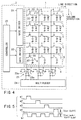
- FIG. 4 is a circuit diagram showing the arrangement of a radiation detector according to the first embodiment of the present invention.
- the radiation detector of the first embodiment comprises an X-ray detection section 1 for detecting incoming radiation, e.g., X-rays, and a read circuit section 2 for reading a signal corresponding to the X-ray intensity detected by the X-ray detection section 1.
- the X-ray detection section 1 has a plurality of pixels 1 which are disposed in a two-dimensional matrix, signal lines 4 for reading signals from the pixels 3, vertical select lines 5 for selecting pixels 3 from which signals are to be read, an adjustment block 6 for adjusting signals output from the pixels 3 to reduce an offset in an integrating circuit (to be described later), and an adjustment block control line 7.
- Each pixel 3 is constructed by a photoelectric conversion element 31 for converting incoming radiation into a charge in an amount corresponding to its intensity, a capacitor 32 for storing the charge generated by the photoelectric conversion element 31, and a thin-film transistor (to be referred to as a read TFT hereinafter) 33 for reading a signal.
- a photoelectric conversion element 31 for converting incoming radiation into a charge in an amount corresponding to its intensity
- a capacitor 32 for storing the charge generated by the photoelectric conversion element 31
- a thin-film transistor to be referred to as a read TFT hereinafter
- the photoelectric conversion element 31 selenium that directly converts X-rays into a charge is used.
- One terminal of the capacitor 32 is connected to ground.
- a terminal 31a of the photoelectric conversion element 31 is maintained at a predetermined potential.
- the element 31 may be a type that indirectly converts X-rays into a charge.
- the element 31 has a scintillator converting X-rays into light and a photodiode converting the light into a charge.
- the adjustment block 6 consists of a plurality of dummy pixels 9.
- the plurality of dummy pixels 9 are respectively connected to the plurality of signal lines 4.
- Each dummy pixel 9 is constructed by an adjustment thin-film transistor (to be referred to as an adjustment TFT hereinafter) 61 and capacitor 62.
- an adjustment TFT an adjustment thin-film transistor
- each dummy pixel 9 unlike the pixel 3 no photoelectric conversion element is present or a photoelectric conversion element, if present, is not electrically connected to the adjustment TFT 61. For this reason, each dummy pixel 9 generates only an offset upon switching of the TFT without generating any signal charge.
- the plurality of adjustment TFTs 61 are commonly connected to the control line 7.
- the adjustment TFTs 61 are formed together with the read TFTs 33 by the same process as the read TFTs 33, and the capacitors 62 are formed together with the capacitors 32 for storing signal charges by the same process as the capacitors 32.
- the adjustment TFTs 61 have approximately the same characteristics as the read TFTs 33.
- the capacitors 62 have approximately the same capacitance as the capacitors 32 for storing signal charges.
- the read circuit section 2 has a gate driver 21 for selectively applying a voltage to the vertical select lines 5 to simultaneously turn on/off the plurality of read TFTs 33, a gate driver 22 for applying a voltage to the control lines 7 to simultaneously turn on/off the plurality of adjustment TFTs 61, integrating circuits 23 for integrating charges read via the read TFTs 33, a multiplexer 24 for sequentially selecting signals amplified by the integrating circuits 23, and a controller 25 for controlling the respective building components such as the gate drivers 21 and 22, multiplexer 24, and the like of the read circuit section 2.
- Each integrating circuit 23 has an amplifier 23a for amplifying a signal read via the read TFT 33, and an integrating capacitor 23b.
- the controller 25 controls the gate driver 21 to selectively apply an ON voltage to the vertical select lines 5.
- Read TFTs 33 connected to a vertical select line 5 which is applied with the ON voltage are simultaneously turned on. When read TFTs 33 are ON, signal charges stored in corresponding capacitors 32 are read onto corresponding signal lines 4.
- the controller 25 controls the gate driver 21 to selectively apply an OFF voltage to the vertical select lines 5.
- Read TFTs 33 connected to a vertical select line 5 which is applied with the OFF voltage are simultaneously turned off. When read TFTs 33 are turned off, the read of signal charges from the capacitors 32 stops.
- the controller 25 controls the gate driver 22 so that the adjustment TFTs 61 are turned on/off 180° out of phase with the read TFTs 33. That is, when the ON voltage is applied to a given vertical select line 5, the OFF voltage is applied to the control line 7 in synchronism with that ON voltage; when the OFF voltage is applied to a given vertical select line 5, the ON voltage is applied to the control line 7 in synchronism with that OFF voltage.
- the controller 25 supplies a reset signal to a reset control line 8 during a period other than a period including the OFF period of the adjustment TFTs 61, thus resetting the integrating circuits 23.
- the gate driver 21 switches the voltages of control signals a1, a2, a3, a4, ... respectively corresponding to the plurality of vertical select line 5 to an ON voltage in turn.
- the read TFTs 33 are sequentially turned on in units of lines.
- the gate driver 22 switches the voltage of a control signal b1 of the control line 7 to an OFF voltage in synchronism with the voltage switching timings of the control signals a1, a2, a3, a4, ....
- the amplitude of the control signal b1 is set to be substantially equivalent to that of the control signal a1 (a2, a3, a4).
- the gate driver 22 applies an OFF voltage to the adjustment block control line 7 connected to the gates of the adjustment TFTs 61 to turn them off under the control of the controller 25.
- the gate driver 21 applies an ON voltage to the first vertical select line 5 to turn on the read TFTs 33 of the pixels 3 connected to that vertical select line 5.
- the gate driver 21 applies an ON voltage to the first vertical select line 5 to turn on the read TFTs 33 of the pixels 3 connected to that vertical select line 5.
- the gate driver 21 switches, e.g., the control signal a1 to an OFF voltage and, at substantially the same time, the gate driver 22 applies an ON voltage as the control signal b1 to turn on the adjustment TFTs 61.
- the controller 25 supplies a reset signal c1 to the reset control line 8 to reset the integrating circuits 23 during periods before and after the predetermined read time.
- capacitors 91 and 92 as an electrically equivalent circuit are respectively formed between the gate of each read TFT 33 and the signal line 4, and between the gate of each adjustment TFT 61 and the signal line 4, as shown in FIG. 7.
- an output waveform d1 from each integrating amplifier 23a drops by an offset ⁇ Vout ⁇ sub across the adjustment TFT 61, since the adjustment TFT 61 is disconnected from the signal line 4 when the control signal b1 changes from ON to OFF.
- each read TFT 33 is connected to the signal line 4, and the output waveform d1 rises by an offset ⁇ Vout across that read TFT 33, which is substantially equal to the offset ⁇ Vout ⁇ sub, and further rises by a detection signal Vout in accordance with a predetermined time constant.
- each adjustment TFT 61 is connected to the signal line 4, the output waveform d1 rises by the offset ⁇ Vout ⁇ sub, and the controller 25 then supplies a reset signal c1 to the reset control line 8 to reset the output waveform d1 to zero level.
- each read TFT is driven to be turned on once during a vertical scan period, while the adjustment TFT is driven to be turned on once during a horizontal scan period.
- the adjustment TFTs 61 and the read TFTs 33 of the respective pixels operate 180° out of phase with each other, their offset voltage cancel each other. As a result, an offset voltage produced upon switching can be practically reduced. Therefore, upon detecting a weak signal in, e.g., fluoroscopy, since a signal can be sufficiently amplified without wasting the dynamic range of each integrating circuit 23, the S/N ratio also improves.
- the conventional manufacturing technique can be used in array design, the detector can be easily manufactured without adding any new processes.
- FIG. 8 is a timing chart for explaining the operation of a radiation detector according to the second embodiment.
- the second embodiment is different from the aforementioned first embodiment in that two vertical select lines 5 are simultaneously turned on to simultaneously read signal charges from a pair of neighboring pixels 3 in the column direction.
- FIG. 9 is a circuit diagram of a radiation detector according to the third embodiment of the present invention
- FIG. 10 is a timing chart for explaining the operation of the radiation detector shown in FIG. 9.
- a characteristic feature of the third embodiment lies in that two dummy pixels 9 are connected to each of a plurality of signal lines 4.
- the radiation detector of the third embodiment comprises an X-ray detection section 1A and read circuit section 2A.
- the X-ray detection section 1A has a plurality of pixels 3, a plurality of signal lines 4, a plurality of vertical select lines 5, adjustment block 6A, and adjustment block control lines 7 for controlling the adjustment block 6A.
- Each pixel 3 has a photoelectric conversion element 31, capacitor 32, and read TFT 33.
- the adjustment block 6A has a plurality of dummy pixels 9. Two dummy pixels 9 are connected to each signal line 4. More specifically, two lines of adjustment TFTs 61 are connected parallel to each other, and the adjustment block control lines 7 are connected to the adjustment TFTS 61 of these lines.
- the read circuit section 2A has a gate driver 21A, gate driver 22A, integrating circuits 23 each having an integrating amplifier 23a and integrating capacitor 23b, multiplexer 24, and controller 25A.
- the gate driver 21A supplies control signals a5 (a6, a7, a8) to the read TFTs 33 connected to the first to fourth lines via the vertical select lines 5 to sequentially turn them on/off
- the gate driver 22A supplies control signals b2 (b3) to the adjustment TFTs 61 connected to the respective lines via the adjustment block control lines 7 to turn on/off the adjustment TFTs 61 in correspondence with the ON/OFF states of the read TFTs 33.
- the gate driver 22A sets OFF voltages as the control signals b2 and b3 to be sent on the two adjustment block control lines 7, and at substantially the same time, the gate driver 21A sets ON voltages as the control signals a5 and a6 to be sent on two, e.g., first and second, vertical select lines 5.
- the gate driver 21A switches the control signals a5 and a6 to OFF voltages, the gate driver 22A switches the control signals b2 and b3 to ON voltage at substantially the same time, and the controller 25A resets the integrating circuits 23.
- the gate driver 22A switches the control signals b2 and b3 to OFF voltages again, and the gate driver 21A switches the control signals a7 and a8 to be sent on two, i.e., third and fourth, vertical select lines 5 to ON voltages, thereby reading signals of these lines.
- the gate driver 22A switches the control signals b2 and b3 to OFF voltages again, and the gate driver 21A switches the control signals a7 and a8 to be sent on two, i.e., third and fourth, vertical select lines 5 to ON voltages, thereby reading signals of these lines.
- the gate ON voltage Von and gate OFF voltage Voff to be applied to the gate of each read TFT 33 respectively become equal to the gate ON voltage Von ⁇ sub and gate OFF voltage Voff ⁇ sub to be applied to the gate of each adjustment TFT 61.
- these sets of gate ON and OFF voltages have equal differences.
- FIG. 11 is a timing chart for explaining the operation of a radiation detector according to the fourth embodiment of the present invention.
- the fourth embodiment is different from the third embodiment mentioned above in that a vertical select line to be driven is selected one by one.
- the gate driver 21A supplies control signals a9 (a10, a11, a12) to the read TFTs 33 connected to the first to fourth lines via corresponding vertical select lines 5 to sequentially turn them on/off
- the gate driver 22A supplies control signals b4 (b5) to the adjustment TFTs 61 of the respective lines via the adjustment block control lines 7 to turn on/off the adjustment TFTs 61 in correspondence with the ON/OFF states of the read TFTs 33.
- the gate driver 22A sets an OFF voltage as the control signal b4 to be sent on the first adjustment block control line 7 and, at substantially the same time, the gate driver 21A sets an ON voltage as the control signal a9 to be sent on, e.g., the first vertical select line 5.
- the gate driver 21A switches the control signal a9 to an OFF voltage
- the gate driver 22A switches the control signal b4 to an ON voltage at substantially the same time
- the controller 25A resets the integrating circuits 23.
- the gate driver 22 maintains the control signal b4 as an OFF voltage and switches the control signal b5 to an OFF voltage in turn and, at substantially the same time, the gate driver 21A switches the control signal a10 to be sent on the second vertical select line 5 to an ON voltage, thus reading signals of this line.
- control signal b4 is switched to an OFF voltage and the control signal all to be sent on the third vertical select line 5 are switched to an ON voltage to read charges from the pixels of that line.
- control signal b5 is switched to an OFF voltage and the control signal a12 to be sent on the fourth vertical select line 5 are switched to an ON voltage to read charges from the pixels of that line.
- the gate driver 22A alternately switches the control signals b4 and b5 to OFF voltages in correspondence with the charge read timings from the pixels of the individual lines. By repeating the aforementioned operations, one image is read.
- the time required between the ON and OFF timings of the adjustment TFT 61 is several ⁇ sec, while the driving method of the fourth embodiment shown in FIG. 11 requires several ten ⁇ sec.
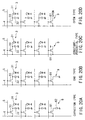
- FIG. 12 is a timing chart for explaining the operation of a radiation detector according to the fifth embodiment of the present invention.
- the fifth embodiment is different from the aforementioned fourth embodiment in that the OFF period of the adjustment TFTs 61 of one line is set to include the read time of the read TFTs 33 for two lines, and the adjustment TFTs 61 of the two lines are alternately turned on/off. Since other arrangements are the same as those in the fourth embodiment, a detailed description thereof will be omitted.
- the gate driver 21A supplies control signals a13 (a14, a15, a16) to the read TFTs 33 connected to the first to fourth lines via corresponding vertical select lines 5 to sequentially turn them on/off
- the gate driver 22A supplies control signals b6 (b7) to the adjustment TFTs 61 of the respective lines via the adjustment block control lines 7 to turn on/off the adjustment TFTs 61 in correspondence with the ON/OFF states of the read TFTs 33.
- the gate driver 22A sets an OFF voltage as the control signal b6 to be sent on the first adjustment block control line 7 and, at substantially the same time, the gate driver 21A sets an ON voltage as the control signal a13 to be sent on, e.g., the first vertical select line 5.
- the gate driver 21A switches the control signal a13 to an OFF voltage
- the gate driver 22A maintains the control signal b6 to be the OFF voltage and switches the control signal b7 to an ON voltage at substantially the same time
- the controller 25A resets the integrating circuits 23.
- the gate driver 22A maintains the control signal b6 to be the OFF voltage and switches the control signal b7 to an OFF voltage and, at substantially the same time, the gate driver 21A switches the control signal a14 to be sent on the second vertical select line 5 to an ON voltage, thus reading signals of this line.
- the gate driver 22A maintains the control signal b7 to be the OFF voltage and switches the control signal b6 to an OFF voltage and, at substantially the same time, the gate driver 21A switches the control signal a15 to be sent on the third vertical select line 5 to an ON voltage, thus reading signals of this line.
- the gate driver 22A maintains the control signal b6 to be the OFF voltage and switches the control signal b7 to an OFF voltage and, at substantially the same time, the gate driver 21A switches the control signal a16 to be sent on the fourth vertical select line 5 to an ON voltage, thus reading signals of this line.
- the gate driver 22A alternately sets OFF voltages as the control signals b6 and b7 in correspondence with the charge read timings of the pixels connected to the respective lines. By repeating the aforementioned operations, one image is read.
- the capacitances Cgs and Cgs ⁇ sub of the capacitors 91 and 92 are equal to each other.
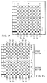
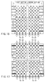
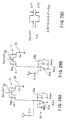
- a capacitor 62 is connected to each adjustment TFT 61, as shown in FIGS. 1 and 13A.
- one terminal of the adjustment TFT 61 may be connected to ground.
- one terminal of the adjustment TFT 61 may be maintained at a constant potential.
- one terminal of the adjustment TFT 61 may be open.
- the detector is driven to simultaneously turn on two vertical select lines 5 to read two pixels at the same time.
- three or more (n) vertical select lines 5 may be turned on at the same time to read n pixels simultaneously.
- the detector is driven to simultaneously turn on two vertical select lines to read two pixels at the same time.
- the detector may be driven to simultaneously turn on n vertical select lines. In this case, voltages are applied so that the difference between the gate ON and OFF voltages applied to the gate of each adjustment TFT becomes n times.
- the influence of offset voltages produced upon switching of the read TFTs 32 is minimized by adjusting the gate ON voltage Von and gate OFF voltage Voff to be supplied to the gate of each adjustment TFT 61.
- the adjustment TFTs of two lines are alternately turned on/off to select the vertical select lines one by one.
- the adjustment block control line 7 connected to the gates of the adjustment TFTs connected to one line may be kept OFF, and the adjustment TFTs of the other line may be driven in the same manner as in the first embodiment, thereby selecting the vertical select lines one by one.
- each adjustment TFT 61 which is opposite to the signal line 4, is connected to the capacitor, but may be open (see FIG. 13D).
- the adjustment TFT 61 may be connected to ground or a constant potential, or may be open without connecting anything), in place of the capacitor as in the first embodiment (see FIGS. 13A to 13D).
- an array of a plurality of pixels 3 and a dummy pixel 9 is designed to form one section.
- an array of a plurality of pixels 3 and dummy pixel 9 is designed to form a plurality of sections.
- two or four sections are formed.
- signals may be read from the two, up and down directions, or the vertical select lines may be driven from the two, right and left directions. Since signals on the vertical select lines 5 suffer differences in the way they become blunt in units of sections, the adjustment block control lines 7 must be independently controlled in units of sections. Also, a plurality of adjustment controllers may be connected to a single signal line 4.
- the dummy pixel (adjustment block) 9 which is similar to a normal pixel is connected to the adjustment block control line 7.
- a characteristic feature of the dummy pixel 9 is that it does not store any signal charge. When any signal charge is stored in this dummy pixel 9, an offset of the TFT in each pixel 3 cannot be normally canceled. For this reason, the dummy pixel 9 has no photoelectric conversion element or a photoelectric conversion element is not connected to the TFT if it has a photoelectric conversion element.
- the adjustment TFT preferably has the same structure as the read TFT, and a structure in which capacitances that are involved in generation of charge injection as a cause of an offset, i.e., the capacitance between the signal line 4 and vertical select line 5 and the capacitance between the signal line 4 and adjustment block control line 7 are equal to each other (FIGS. 20A to 20D).
- the pixel capacitance of the dummy pixel 9 some choices are available: the TFT of the dummy pixel has a pixel capacitance; the TFT is connected to a constant potential; the TFT has an open terminal; and so forth (FIG. 20D).
- the signals on the vertical select lines 5 and those on the adjustment block control lines 7 in the individual sections must be adjusted. This adjustment is implemented by controlling the ON/OFF switching timing, time constant, amplitude, and voltage value. Ideally, the time constants and timings of the signals on the vertical select lines 5 and adjustment block control lines 7 should match, but it is difficult to match them perfectly. Also, correction must be done in units of signals on a plurality of vertical select lines 5 and at least one adjustment block control line 7, and it is hard to match the timing and time constant with those of signals on all the vertical select lines 6 using a predetermined adjustment block control line 7, in consideration of variations of the vertical select lines 5. In practice, the signals need only be adjusted not to be saturated in the subsequent circuits such as integrating circuits and the like. In this case, the output value of each integrating circuit has a peak in a transient state, and the signals need only be adjusted so that the peak does not reach saturation.
- the amplitude of the signal on each adjustment block control line 7 varies depending on the number of vertical select lines 5 to be turned on at the same time, and the associated capacitance.
- the associated capacitance is that between the vertical select line 5 and signal line 4.
- Cgs be this capacitance
- Cgs ⁇ sub be the capacitance between the adjustment block control line 7 and signal line 4
- Von and Voff be the ON and OFF voltages of the vertical select line 5
- Von ⁇ sub and Voff ⁇ sub be the ON and OFF voltages of the adjustment block control line 7.
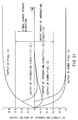
- the integrating circuit If no signal is stored in a given pixel 3, the integrating circuit generates nearly zero output. When a signal charge is stored in only one direction, and the integrating circuit can generate both positive and negative outputs, nearly half the range is used, i.e., the dynamic range is wasted. Hence, the ON and OFF voltages of the adjustment block control line 7 are adjusted to generate a charge having a polarity opposite to that of a signal charge, thus fully utilizing the dynamic range of the integrating circuit (FIG. 22).
- the ON and OFF voltages Von ⁇ sub, Voff ⁇ sub of the adjustment block control line 7 are shifted to Von ⁇ sub', Voff ⁇ sub' on the basis of shifting voltage ⁇ Von ⁇ off ⁇ sub.
- ⁇ Von ⁇ sub' - Voff ⁇ sub' ⁇ Von ⁇ sub - Voff ⁇ sub + ⁇ Von ⁇ off ⁇ sub
- the shifting voltage ⁇ Von ⁇ off ⁇ sub is set on the basis of the capacitance Cint of the integrating circuit, the offset voltage ⁇ V, and the Cgs ⁇ sub.
- ⁇ V ⁇ Cint ⁇ Von ⁇ off ⁇ sub ⁇ Cgs sub
- the amplitude can be determined by the above relation.
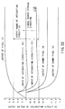
- the ON/OFF voltage values of the adjustment block control line 7 even the ON voltage can be set to be sufficiently small so that the adjustment control TFT can always operate in the OFF region (a region with a small leakage current: ⁇ V better in FIG. 23). With this control, the influence of the interior of the dummy pixel 9 connected to the adjustment block control line 7 can be minimized.
- the gate driver that applies signals to the vertical select lines 5 suffers variations, or the distances from the pixels to the integrating circuits are different, the offset cannot often be satisfactorily corrected by the adjustment block control line 7 that is simply repetitively turned on/off. In such case, when the voltage of the adjustment control line 7 is adjusted in units of vertical select lines, slight variations can also be corrected.
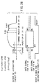
- a memory 26 for holding driving information (time constants, timings) of the adjustment block control line 7 in units of vertical select lines 5 is provided, and voltages corresponding to the stored information must be generated under the control of the controller 25.
- the output waveform is sampled to extract signal components from the output of each integrating circuit.
- the sampling method the following two methods are available.
- the output waveform is sampled at two timings, i.e., a timing (S/H0) immediately before the read TFT is turned on and a timing (S/H1) immediately before the read TFT is turned off, and their difference is output.
- a timing (S/H0) immediately before the read TFT is turned on and a timing (S/H1) immediately before the read TFT is turned off and their difference is output.
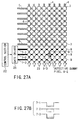
- the output waveform is sampled at two timings, i.e., a timing (S/H0) immediately before the read TFT is turned on, and a timing (S/H2) after the read TFT is turned off, and their difference is output (as a signal), as shown in FIG. 26.
- a timing (S/H0) immediately before the read TFT is turned on and a timing (S/H2) after the read TFT is turned off, and their difference is output (as a signal), as shown in FIG. 26.
- the signal charge transfer time from each pixel becomes short, but since ON/OFF operations of the read TFT are included, charge injection by the read TFT is canceled by its own ON/OFF operations, thus canceling variations of the individual read TFTs.
- the integrating capacitor of each integrating circuit is small, the signal is saturated when the read TFT is turned on. Saturation caused by charge injection can be avoided by driving the adjustment TFT. That is, temporal saturation can be canceled by those of the vertical select lines 5 and adjustment block control line 7, and variations due to individual differences can be canceled by charge injections of the read and adjustment TFTs by respectively turning on/off those TFTs. In this manner, any in-plane distribution can be suppressed.
- one section includes a plurality of adjustment block control lines 7, if some of (not all) those adjustment block control lines 7 include any defective pixels and defective lines, such control lines 7 are not used, and the remaining adjustment block control lines 7 compensate for imperfect canceling of charge injection.
- the amplitudes of the adjustment block control lines 7 used are amplified. If an adjustment block control line 7 including some defective pixel is used, the signal line 4 corresponding to the defective pixel is not normally corrected, and appears as a defective line in an image. That is, by inhibiting such defective adjustment block control line 7 from being used, the influence on the image can be minimized.
- a method of canceling charge injection by directly inputting a charge to the input terminal of the integrating circuit is available.
- one terminal of a capacitor is connected to the input terminal of the integrating circuit, and the voltage at the other terminal of the capacitor is changed, thereby inputting a charge.
- a method of changing the voltage a method of supplying a constant pulse signal is known. As in the above case, when the timing, time constant, and amplitude are changed in units of pixels, more accurate correction can be achieved. In such case, a memory for saving pixel information and a driver for generating signals in accordance with saved information are required.
- FIG. 29 shows the arrangement of an X-ray diagnosis apparatus to which the radiation detector is applied.
- a radiation detector 301 is disposed on a side opposite to an X-ray generation source 303 for generating X-rays to sandwich a bed 302 on which a patient lies down therebetween.
- the X-ray generation source 303 and radiation detector 301 are held by a C-arm stand 310 to be able to arbitrarily change the angle with respect to the patient.
- the angle is controlled by a system control unit 304.
- the system control unit 304 is connected to the inputting device 309 to input the fluoroscopy/shot selecting command.
- the system control unit 304 controls X-ray radiation conditions and image acquisition conditions of the detector 301 in accordance with the input command.
- a display 307 displays images acquired by the radiation detector 301, and those processed by an image processing unit 306.
- An image storing unit 308 stores images acquired by the radiation detector 301, and those processed by the image processing unit 306.
- the system control unit 304 supplies a control signal for synchronizing the X-ray generation sequence of the X-ray generation source 303 with the image acquisition sequence of the radiation detector 301 to the X-ray generation source 303 and radiation detector 301. Also, the system control unit 304 selects the relationship between the driving speed and resolution in accordance with the input fluoroscopy/shot selecting command, and supplies control signals for setting the number of vertical select lines 5 to be simultaneously turned on, the number of control lines 7 to be simultaneously turned on, the driving voltage of each vertical select line 5, and that of each control line 7 to the controller 22 of the radiation detector 301.
- the number of vertical select lines 5 simultaneously turned on, the number of control lines 7 simultaneously turned on, the driving voltage of each vertical select line 5, and the driving voltage of each control line 7 may be input by the input device 309.
- These control signals can be either signals for directly determining the voltages and the numbers of lines to be driven, and signals for indirectly determining them by selecting a driving mode of the detector 301. Note that the indirect control signals are converted into direct signals by the controller 25 in the detector 301.
- optimal offset cancel functions in units of various driving modes can be provided to the detector 301, and images that the operator wants can be acquired.
Landscapes
- Engineering & Computer Science (AREA)
- Multimedia (AREA)
- Signal Processing (AREA)
- Measurement Of Radiation (AREA)
- Solid State Image Pick-Up Elements (AREA)
- Transforming Light Signals Into Electric Signals (AREA)
- Facsimile Heads (AREA)
- Apparatus For Radiation Diagnosis (AREA)
- Closed-Circuit Television Systems (AREA)
- Light Receiving Elements (AREA)
Applications Claiming Priority (4)
| Application Number | Priority Date | Filing Date | Title |
|---|---|---|---|
| JP16021399 | 1999-06-07 | ||
| JP16021399 | 1999-06-07 | ||
| JP2000108099A JP2001056382A (ja) | 1999-06-07 | 2000-04-10 | 放射線検出器及び放射線診断装置 |
| JP2000108099 | 2000-04-10 |
Publications (3)
| Publication Number | Publication Date |
|---|---|
| EP1067606A2 true EP1067606A2 (fr) | 2001-01-10 |
| EP1067606A3 EP1067606A3 (fr) | 2002-06-05 |
| EP1067606B1 EP1067606B1 (fr) | 2012-07-04 |
Family
ID=26486769
Family Applications (1)
| Application Number | Title | Priority Date | Filing Date |
|---|---|---|---|
| EP00108384A Expired - Lifetime EP1067606B1 (fr) | 1999-06-07 | 2000-04-17 | Détecteur de rayonnement |
Country Status (4)
| Country | Link |
|---|---|
| US (1) | US6696687B1 (fr) |
| EP (1) | EP1067606B1 (fr) |
| JP (1) | JP2001056382A (fr) |
| CN (1) | CN1183390C (fr) |
Cited By (5)
| Publication number | Priority date | Publication date | Assignee | Title |
|---|---|---|---|---|
| EP1378200A1 (fr) * | 2002-06-26 | 2004-01-07 | Kabushiki Kaisha Toshiba | Appareil radiodiagnostique |
| EP1378942A1 (fr) * | 2002-07-05 | 2004-01-07 | Kabushiki Kaisha Toshiba | Détecteur de radiation avec correction du réglage |
| EP1850582A1 (fr) | 2006-04-27 | 2007-10-31 | Canon Kabushiki Kaisha | Appareil d'imagerie, appareil d'imagerie à radiation et système d'imagerie à radiation |
| CN105284104A (zh) * | 2013-06-11 | 2016-01-27 | 浜松光子学株式会社 | 固体摄像装置 |
| EP4177643A4 (fr) * | 2020-07-01 | 2024-03-27 | Canon Electron Tubes & Devices Co., Ltd. | Détecteur de rayonnements |
Families Citing this family (42)
| Publication number | Priority date | Publication date | Assignee | Title |
|---|---|---|---|---|
| JP2002151669A (ja) * | 2000-11-14 | 2002-05-24 | Toshiba Corp | X線撮像装置 |
| JP4723767B2 (ja) * | 2001-09-13 | 2011-07-13 | 株式会社東芝 | X線画像診断装置 |
| US6989538B2 (en) * | 2003-07-22 | 2006-01-24 | General Electric Co. | Method of reducing recovery time in an x-ray detector |
| US7550732B2 (en) * | 2004-09-30 | 2009-06-23 | Fujifilm Corporation | Radiation image detector |
| US7302039B2 (en) * | 2005-02-24 | 2007-11-27 | Canon Kabushiki Kaisha | Radiography apparatus, radiography system, and control method thereof |
| JP4773768B2 (ja) * | 2005-08-16 | 2011-09-14 | キヤノン株式会社 | 放射線撮像装置、その制御方法及び放射線撮像システム |
| JPWO2008012897A1 (ja) * | 2006-07-27 | 2009-12-17 | 株式会社島津製作所 | 光または放射線撮像装置 |
| JP5406473B2 (ja) | 2007-07-19 | 2014-02-05 | キヤノン株式会社 | 放射線検出装置 |
| JP4949964B2 (ja) * | 2007-08-10 | 2012-06-13 | 富士フイルム株式会社 | 放射線画像検出器 |
| JP5171431B2 (ja) * | 2008-06-26 | 2013-03-27 | 株式会社ジャパンディスプレイウェスト | 光電変換装置、放射線撮像装置及び放射線検出装置 |
| US9545239B2 (en) * | 2008-07-28 | 2017-01-17 | Orthosoft Inc. | X-ray detection device for C-arm tracker and method |
| WO2010058369A2 (fr) * | 2008-11-24 | 2010-05-27 | Philips Intellectual Property & Standards Gmbh | Détecteur de rayons x |
| WO2011055277A2 (fr) * | 2009-11-03 | 2011-05-12 | Koninklijke Philips Electronics N.V. | Unité de détection servant à détecter un rayonnement électromagnétique |
| JP5335006B2 (ja) * | 2010-02-26 | 2013-11-06 | 三菱電機株式会社 | 赤外線固体撮像素子 |
| CN102792184B (zh) * | 2010-03-09 | 2014-10-29 | 株式会社岛津制作所 | 二维阵列x射线检测器的检查方法 |
| JP4779054B1 (ja) | 2010-03-31 | 2011-09-21 | 富士フイルム株式会社 | 固体撮像素子及び撮像装置 |
| JP2012090032A (ja) * | 2010-10-19 | 2012-05-10 | Toshiba Corp | ラインアーチファクト検出器及びその検出方法 |
| JP2012130406A (ja) * | 2010-12-20 | 2012-07-12 | Shimadzu Corp | 二次元画像撮影装置 |
| JP5676503B2 (ja) | 2011-02-01 | 2015-02-25 | 富士フイルム株式会社 | 放射線画像撮影装置、放射線画像撮影装置の制御プログラム、及び放射線画像撮影装置の制御方法 |
| JP6021344B2 (ja) * | 2011-05-12 | 2016-11-09 | キヤノン株式会社 | 固体撮像装置、固体撮像装置の駆動方法、固体撮像システム |
| JP5847472B2 (ja) * | 2011-07-20 | 2016-01-20 | キヤノン株式会社 | 検出装置及び検出システム |
| JP5583191B2 (ja) * | 2011-11-25 | 2014-09-03 | 富士フイルム株式会社 | 放射線画像検出装置およびその作動方法 |
| TWI488500B (zh) * | 2011-12-23 | 2015-06-11 | Ind Tech Res Inst | X射線主動式畫素感測器讀取電路與讀取方法 |
| WO2013133136A1 (fr) * | 2012-03-09 | 2013-09-12 | 富士フイルム株式会社 | Dispositif de radiographie, système de radiographie, procédé de commande de dispositif de radiographie et programme de commande de dispositif de radiographie |
| KR20130104563A (ko) * | 2012-03-14 | 2013-09-25 | 삼성디스플레이 주식회사 | 유기 발광 표시 장치의 어레이 시험 장치 및 시험 방법, 및 유기 발광 표시 장치의 제조 방법 |
| JP6174849B2 (ja) * | 2012-08-10 | 2017-08-02 | キヤノン株式会社 | 放射線撮像装置及び放射線撮像システム |
| JP2014081358A (ja) * | 2012-09-27 | 2014-05-08 | Fujifilm Corp | 放射線画像検出装置 |
| WO2014070719A1 (fr) * | 2012-10-30 | 2014-05-08 | Carestream Health, Inc. | Compensation d'injection de charge pour détecteurs radiographiques numériques |
| DE102013205461A1 (de) * | 2013-03-27 | 2014-10-16 | Siemens Aktiengesellschaft | Detektoreinheit |
| US9264639B2 (en) | 2014-02-07 | 2016-02-16 | Rambus Inc. | Feedthrough-compensated image sensor |
| JP6404661B2 (ja) * | 2014-09-29 | 2018-10-10 | 東芝電子管デバイス株式会社 | 放射線検出器用アレイ基板、および放射線検出器 |
| JP6512909B2 (ja) * | 2015-04-09 | 2019-05-15 | キヤノン株式会社 | 放射線撮像装置および放射線撮像システム |
| US10306168B2 (en) * | 2015-05-04 | 2019-05-28 | Semiconductor Energy Laboratory Co., Ltd. | Semiconductor device, imaging system, and electronic device |
| TWI713367B (zh) * | 2015-07-07 | 2020-12-11 | 日商半導體能源研究所股份有限公司 | 成像裝置及其運作方法 |
| US10209374B2 (en) * | 2015-07-13 | 2019-02-19 | Sharp Kabushiki Kaisha | Radiation detector |
| JP7624387B2 (ja) * | 2019-04-08 | 2025-01-30 | ソニーセミコンダクタソリューションズ株式会社 | センサチップ及び電子機器 |
| KR102831446B1 (ko) * | 2019-09-17 | 2025-07-09 | 에스케이하이닉스 주식회사 | 이미지 센싱 장치 |
| TWI785342B (zh) * | 2020-06-11 | 2022-12-01 | 睿生光電股份有限公司 | 輻射偵測裝置 |
| CN113805221B (zh) * | 2020-06-11 | 2024-09-27 | 睿生光电股份有限公司 | 辐射检测装置 |
| CN118647893A (zh) * | 2022-02-09 | 2024-09-13 | 国立大学法人静冈大学 | 距离测量装置及距离测量方法 |
| JP2024061977A (ja) | 2022-10-24 | 2024-05-09 | キヤノン株式会社 | 放射線撮像装置及び放射線撮像装置の制御方法 |
| CN115855271B (zh) * | 2023-02-22 | 2023-05-23 | 昆明钍晶科技有限公司 | 一种具有大电荷处理能力的读出电路及红外热成像仪 |
Family Cites Families (24)
| Publication number | Priority date | Publication date | Assignee | Title |
|---|---|---|---|---|
| US3949162A (en) * | 1974-02-25 | 1976-04-06 | Actron Industries, Inc. | Detector array fixed-pattern noise compensation |
| FR2593987B1 (fr) * | 1986-01-24 | 1989-08-04 | Thomson Csf | Dispositif photosensible a l'etat solide |
| JPS637082A (ja) * | 1986-06-27 | 1988-01-12 | Nikon Corp | アドレス方式のイメ−ジセンサの制御方法 |
| JPS6328167A (ja) * | 1986-07-22 | 1988-02-05 | Fuji Xerox Co Ltd | イメ−ジセンサの駆動装置 |
| JPS63181370A (ja) * | 1987-01-22 | 1988-07-26 | Tokyo Electric Co Ltd | 原稿読取り装置 |
| JPH01109975A (ja) * | 1987-10-23 | 1989-04-26 | Nikon Corp | イメージセンサの読出回路 |
| JPH01185066A (ja) * | 1988-01-19 | 1989-07-24 | Sanyo Electric Co Ltd | リニアイメージセンサ及びリニアイメージセンサによる画像読取方式 |
| JPH01276887A (ja) * | 1988-04-27 | 1989-11-07 | Fuji Xerox Co Ltd | 画像読取装置 |
| JP2803098B2 (ja) * | 1988-08-09 | 1998-09-24 | 富士ゼロックス株式会社 | 画像読取装置 |
| JPH0728861B2 (ja) * | 1989-01-09 | 1995-04-05 | 株式会社東芝 | X線ct装置 |
| DE4002431A1 (de) * | 1990-01-27 | 1991-08-01 | Philips Patentverwaltung | Sensormatrix |
| JPH06105069A (ja) * | 1992-09-17 | 1994-04-15 | Kanegafuchi Chem Ind Co Ltd | 画像読取方法及びその装置 |
| JPH06113136A (ja) * | 1992-09-30 | 1994-04-22 | Fuji Xerox Co Ltd | 画像読取装置及びその画像読取方法 |
| US5319206A (en) * | 1992-12-16 | 1994-06-07 | E. I. Du Pont De Nemours And Company | Method and apparatus for acquiring an X-ray image using a solid state device |
| DE4426451C2 (de) * | 1994-07-26 | 1998-07-16 | Siemens Ag | Röntgendiagnostikeinrichtungen mit einem Festkörperbildwandler |
| JPH0946597A (ja) * | 1995-07-31 | 1997-02-14 | Sony Corp | 固体撮像装置およびその駆動方法 |
| US5818898A (en) * | 1995-11-07 | 1998-10-06 | Kabushiki Kaisha Toshiba | X-ray imaging apparatus using X-ray planar detector |
| JP3415348B2 (ja) * | 1995-11-07 | 2003-06-09 | 東芝医用システムエンジニアリング株式会社 | X線撮像装置 |
| US5648660A (en) * | 1996-01-05 | 1997-07-15 | Sterling Diagnostic Imaging, Inc. | Method and apparatus for reducing noise in a radiation capture device |
| GB2318473B (en) * | 1996-10-17 | 2000-11-29 | Sony Corp | Solid state imaging device,signal processing method and camera |
| JP4088986B2 (ja) * | 1997-07-30 | 2008-05-21 | 株式会社島津製作所 | 2次元放射線検出器 |
| JPH1187681A (ja) * | 1997-09-04 | 1999-03-30 | Shimadzu Corp | フラット・パネル形センサ |
| JP3027569B2 (ja) * | 1998-04-14 | 2000-04-04 | 松下電子工業株式会社 | 増幅型固体撮像装置、その駆動方法及び物理量分布検知半導体装置 |
| JP3618232B2 (ja) * | 1998-09-17 | 2005-02-09 | シャープ株式会社 | 固体撮像装置のクランプ回路 |
-
2000
- 2000-04-10 JP JP2000108099A patent/JP2001056382A/ja active Pending
- 2000-04-17 EP EP00108384A patent/EP1067606B1/fr not_active Expired - Lifetime
- 2000-04-18 US US09/550,800 patent/US6696687B1/en not_active Expired - Lifetime
- 2000-06-06 CN CNB001179764A patent/CN1183390C/zh not_active Expired - Fee Related
Cited By (12)
| Publication number | Priority date | Publication date | Assignee | Title |
|---|---|---|---|---|
| EP1378200A1 (fr) * | 2002-06-26 | 2004-01-07 | Kabushiki Kaisha Toshiba | Appareil radiodiagnostique |
| EP1525847A1 (fr) * | 2002-06-26 | 2005-04-27 | Kabushiki Kaisha Toshiba | Appareil radiodiagnostique |
| EP1378942A1 (fr) * | 2002-07-05 | 2004-01-07 | Kabushiki Kaisha Toshiba | Détecteur de radiation avec correction du réglage |
| US7223980B2 (en) * | 2002-07-05 | 2007-05-29 | Kabushiki Kaisha Toshiba | Radiation detector that adjusts offset component |
| EP1850582A1 (fr) | 2006-04-27 | 2007-10-31 | Canon Kabushiki Kaisha | Appareil d'imagerie, appareil d'imagerie à radiation et système d'imagerie à radiation |
| US7573041B2 (en) | 2006-04-27 | 2009-08-11 | Canon Kabushiki Kaisha | Imaging apparatus, radiation imaging apparatus, and radiation imaging system |
| US7791034B2 (en) | 2006-04-27 | 2010-09-07 | Canon Kabushiki Kaisha | Imaging apparatus, radiation imaging apparatus, and radiation imaging system |
| CN105284104A (zh) * | 2013-06-11 | 2016-01-27 | 浜松光子学株式会社 | 固体摄像装置 |
| EP3010227A4 (fr) * | 2013-06-11 | 2017-02-15 | Hamamatsu Photonics K.K. | Dispositif d'imagerie à semiconducteurs |
| US10090341B2 (en) | 2013-06-11 | 2018-10-02 | Hamamatsu Photonics K.K. | Solid-state imaging device |
| US10685991B2 (en) | 2013-06-11 | 2020-06-16 | Hamamatsu Photonics K.K. | Solid-state imaging device |
| EP4177643A4 (fr) * | 2020-07-01 | 2024-03-27 | Canon Electron Tubes & Devices Co., Ltd. | Détecteur de rayonnements |
Also Published As
| Publication number | Publication date |
|---|---|
| CN1276535A (zh) | 2000-12-13 |
| EP1067606B1 (fr) | 2012-07-04 |
| JP2001056382A (ja) | 2001-02-27 |
| US6696687B1 (en) | 2004-02-24 |
| EP1067606A3 (fr) | 2002-06-05 |
| CN1183390C (zh) | 2005-01-05 |
Similar Documents
| Publication | Publication Date | Title |
|---|---|---|
| EP1067606B1 (fr) | Détecteur de rayonnement | |
| KR101916504B1 (ko) | 방사선 촬상 장치 및 방사선 검지 시스템 | |
| US7087880B2 (en) | Photosensitive device and method for controlling same | |
| US6583398B2 (en) | Image sensor | |
| US8809760B2 (en) | Imaging apparatus, imaging system, method of controlling the apparatus and the system, and program | |
| TW390096B (en) | Physical quantity distribution detection semiconductor device and its driving method | |
| US9172951B2 (en) | Test circuit for testing signal receiving unit, image pickup apparatus, method of testing signal receiving unit, and method of testing image pickup apparatus | |
| US7223980B2 (en) | Radiation detector that adjusts offset component | |
| US8818068B2 (en) | Imaging apparatus, imaging system, method of controlling the apparatus and the system, and program | |
| US8203111B2 (en) | CMOS image sensor pixel with an NMOS charge amplifier | |
| US9197824B2 (en) | Image pickup unit, method of driving image pickup unit, and image pickup display system | |
| KR102065807B1 (ko) | 디지털 방사선 촬영 검출기들을 위한 전하 주입 보상 | |
| WO2011027538A1 (fr) | Appareil de réalisation d'image, système de réalisation d'image, procédé de commande de l'appareil et du système, et programme | |
| JP2008233379A (ja) | 液晶表示装置 | |
| US7915594B2 (en) | X-ray detector and method of driving the same | |
| JPH11502995A (ja) | マルチプレクサ回路 | |
| US20050194624A1 (en) | Photoelectric conversion device and method of driving the same | |
| JP2002199282A (ja) | 光電変換装置、及びその駆動方法 | |
| US6888969B1 (en) | Method and apparatus for preventing image artifacts | |
| KR20200076328A (ko) | 디지털 엑스레이 검출장치 및 그의 구동방법 | |
| JP2010246129A (ja) | 放射線検出器 | |
| JP4646997B2 (ja) | 光電変換装置の駆動方法 | |
| JP5784086B2 (ja) | 撮像装置及び撮像システム、それらの制御方法及びそのプログラム | |
| US6677997B1 (en) | Amplifying solid-state imaging device, and method for driving the same | |
| JP4339151B2 (ja) | 光電変換装置 |
Legal Events
| Date | Code | Title | Description |
|---|---|---|---|
| PUAI | Public reference made under article 153(3) epc to a published international application that has entered the european phase |
Free format text: ORIGINAL CODE: 0009012 |
|
| 17P | Request for examination filed |
Effective date: 20000417 |
|
| AK | Designated contracting states |
Kind code of ref document: A2 Designated state(s): AT BE CH CY DE DK ES FI FR GB GR IE IT LI LU MC NL PT SE |
|
| AX | Request for extension of the european patent |
Free format text: AL;LT;LV;MK;RO;SI |
|
| PUAL | Search report despatched |
Free format text: ORIGINAL CODE: 0009013 |
|
| AK | Designated contracting states |
Kind code of ref document: A3 Designated state(s): AT BE CH CY DE DK ES FI FR GB GR IE IT LI LU MC NL PT SE |
|
| AX | Request for extension of the european patent |
Free format text: AL;LT;LV;MK;RO;SI |
|
| RIC1 | Information provided on ipc code assigned before grant |
Free format text: 7H 01L 27/146 A, 7H 04N 3/15 B, 7H 04N 5/217 B |
|
| AKX | Designation fees paid |
Designated state(s): DE FR NL |
|
| 17Q | First examination report despatched |
Effective date: 20050527 |
|
| REG | Reference to a national code |
Ref country code: DE Ref legal event code: R079 Ref document number: 60047307 Country of ref document: DE Free format text: PREVIOUS MAIN CLASS: H01L0027146000 Ipc: H04N0005361000 |
|
| GRAP | Despatch of communication of intention to grant a patent |
Free format text: ORIGINAL CODE: EPIDOSNIGR1 |
|
| RIC1 | Information provided on ipc code assigned before grant |
Ipc: H04N 5/361 20110101AFI20120102BHEP Ipc: H01L 27/146 20060101ALI20120102BHEP |
|
| GRAS | Grant fee paid |
Free format text: ORIGINAL CODE: EPIDOSNIGR3 |
|
| GRAA | (expected) grant |
Free format text: ORIGINAL CODE: 0009210 |
|
| RIN1 | Information on inventor provided before grant (corrected) |
Inventor name: SAKAGUCHI, TAKUYA Inventor name: NAGAI, SEIICHIRO Inventor name: HONDA, MICHITAKA Inventor name: TANAKA, MANABU Inventor name: TOMISAKI, TAKAYUKI |
|
| AK | Designated contracting states |
Kind code of ref document: B1 Designated state(s): DE FR NL |
|
| RAP1 | Party data changed (applicant data changed or rights of an application transferred) |
Owner name: KABUSHIKI KAISHA TOSHIBA |
|
| REG | Reference to a national code |
Ref country code: DE Ref legal event code: R081 Ref document number: 60047307 Country of ref document: DE Owner name: TOSHIBA MEDICAL SYSTEMS CORPORATION, OTAWARA-S, JP Free format text: FORMER OWNER: KABUSHIKI KAISHA TOSHIBA, KAWASAKI, KANAGAWA, JP |
|
| REG | Reference to a national code |
Ref country code: DE Ref legal event code: R096 Ref document number: 60047307 Country of ref document: DE Effective date: 20120823 |
|
| REG | Reference to a national code |
Ref country code: NL Ref legal event code: T3 |
|
| PLBE | No opposition filed within time limit |
Free format text: ORIGINAL CODE: 0009261 |
|
| STAA | Information on the status of an ep patent application or granted ep patent |
Free format text: STATUS: NO OPPOSITION FILED WITHIN TIME LIMIT |
|
| 26N | No opposition filed |
Effective date: 20130405 |
|
| REG | Reference to a national code |
Ref country code: DE Ref legal event code: R097 Ref document number: 60047307 Country of ref document: DE Effective date: 20130405 |
|
| REG | Reference to a national code |
Ref country code: FR Ref legal event code: PLFP Year of fee payment: 17 |
|
| PGFP | Annual fee paid to national office [announced via postgrant information from national office to epo] |
Ref country code: FR Payment date: 20160309 Year of fee payment: 17 |
|
| PGFP | Annual fee paid to national office [announced via postgrant information from national office to epo] |
Ref country code: NL Payment date: 20160411 Year of fee payment: 17 |
|
| PGFP | Annual fee paid to national office [announced via postgrant information from national office to epo] |
Ref country code: DE Payment date: 20160412 Year of fee payment: 17 |
|
| REG | Reference to a national code |
Ref country code: NL Ref legal event code: PD Owner name: TOSHIBA MEDICAL SYSTEMS CORPORATION; JP Free format text: DETAILS ASSIGNMENT: VERANDERING VAN EIGENAAR(S), OVERDRACHT; FORMER OWNER NAME: KABUSHIKI KAISHA TOSHIBA Effective date: 20160627 |
|
| REG | Reference to a national code |
Ref country code: FR Ref legal event code: TP Owner name: TOSHIBA MEDICAL SYSTEMS CORPORATION, JP Effective date: 20160830 |
|
| REG | Reference to a national code |
Ref country code: DE Ref legal event code: R081 Ref document number: 60047307 Country of ref document: DE Owner name: TOSHIBA MEDICAL SYSTEMS CORPORATION, OTAWARA-S, JP Free format text: FORMER OWNER: KABUSHIKI KAISHA TOSHIBA, TOKYO, JP Ref country code: DE Ref legal event code: R082 Ref document number: 60047307 Country of ref document: DE Representative=s name: KRAMER BARSKE SCHMIDTCHEN PATENTANWAELTE PARTG, DE |
|
| REG | Reference to a national code |
Ref country code: DE Ref legal event code: R119 Ref document number: 60047307 Country of ref document: DE |
|
| REG | Reference to a national code |
Ref country code: NL Ref legal event code: MM Effective date: 20170501 |
|
| REG | Reference to a national code |
Ref country code: FR Ref legal event code: ST Effective date: 20171229 |
|
| PG25 | Lapsed in a contracting state [announced via postgrant information from national office to epo] |
Ref country code: DE Free format text: LAPSE BECAUSE OF NON-PAYMENT OF DUE FEES Effective date: 20171103 Ref country code: NL Free format text: LAPSE BECAUSE OF NON-PAYMENT OF DUE FEES Effective date: 20170501 Ref country code: FR Free format text: LAPSE BECAUSE OF NON-PAYMENT OF DUE FEES Effective date: 20170502 |