EP1067779A2 - Dispositif de prise de vue - Google Patents
Dispositif de prise de vue Download PDFInfo
- Publication number
- EP1067779A2 EP1067779A2 EP00305472A EP00305472A EP1067779A2 EP 1067779 A2 EP1067779 A2 EP 1067779A2 EP 00305472 A EP00305472 A EP 00305472A EP 00305472 A EP00305472 A EP 00305472A EP 1067779 A2 EP1067779 A2 EP 1067779A2
- Authority
- EP
- European Patent Office
- Prior art keywords
- image pickup
- image
- pickup apparatus
- light
- filter
- Prior art date
- Legal status (The legal status is an assumption and is not a legal conclusion. Google has not performed a legal analysis and makes no representation as to the accuracy of the status listed.)
- Withdrawn
Links
- 230000003287 optical effect Effects 0.000 claims description 77
- 230000005540 biological transmission Effects 0.000 claims description 43
- 239000011521 glass Substances 0.000 claims description 13
- 230000008859 change Effects 0.000 claims description 11
- 238000012937 correction Methods 0.000 claims description 7
- 238000005520 cutting process Methods 0.000 claims description 5
- 239000000463 material Substances 0.000 claims description 5
- 230000005855 radiation Effects 0.000 claims description 5
- 229920005989 resin Polymers 0.000 claims description 2
- 239000011347 resin Substances 0.000 claims description 2
- 238000012545 processing Methods 0.000 description 68
- 230000003595 spectral effect Effects 0.000 description 30
- 238000003384 imaging method Methods 0.000 description 17
- 238000009826 distribution Methods 0.000 description 13
- 238000000034 method Methods 0.000 description 9
- 230000004075 alteration Effects 0.000 description 7
- 238000001514 detection method Methods 0.000 description 7
- 210000001747 pupil Anatomy 0.000 description 7
- -1 rare-earth metal ions Chemical class 0.000 description 7
- 229910052727 yttrium Inorganic materials 0.000 description 6
- 230000006835 compression Effects 0.000 description 5
- 238000007906 compression Methods 0.000 description 5
- 230000003247 decreasing effect Effects 0.000 description 5
- 239000004973 liquid crystal related substance Substances 0.000 description 5
- 238000005516 engineering process Methods 0.000 description 4
- 238000009825 accumulation Methods 0.000 description 3
- 230000008901 benefit Effects 0.000 description 3
- 238000006243 chemical reaction Methods 0.000 description 3
- 150000002500 ions Chemical class 0.000 description 3
- 230000004044 response Effects 0.000 description 3
- 238000000926 separation method Methods 0.000 description 3
- 239000010409 thin film Substances 0.000 description 3
- 229910052779 Neodymium Inorganic materials 0.000 description 2
- 239000003086 colorant Substances 0.000 description 2
- 238000010586 diagram Methods 0.000 description 2
- 239000006185 dispersion Substances 0.000 description 2
- 238000002224 dissection Methods 0.000 description 2
- 230000006870 function Effects 0.000 description 2
- 230000012447 hatching Effects 0.000 description 2
- 238000012986 modification Methods 0.000 description 2
- 230000004048 modification Effects 0.000 description 2
- 230000002093 peripheral effect Effects 0.000 description 2
- 229910052761 rare earth metal Inorganic materials 0.000 description 2
- 238000005316 response function Methods 0.000 description 2
- 238000004544 sputter deposition Methods 0.000 description 2
- 238000007740 vapor deposition Methods 0.000 description 2
- VYZAMTAEIAYCRO-UHFFFAOYSA-N Chromium Chemical compound [Cr] VYZAMTAEIAYCRO-UHFFFAOYSA-N 0.000 description 1
- 229910052691 Erbium Inorganic materials 0.000 description 1
- 229910052689 Holmium Inorganic materials 0.000 description 1
- 229910052777 Praseodymium Inorganic materials 0.000 description 1
- 230000009471 action Effects 0.000 description 1
- 230000002547 anomalous effect Effects 0.000 description 1
- 229910001179 chromel Inorganic materials 0.000 description 1
- 229910052804 chromium Inorganic materials 0.000 description 1
- 239000011651 chromium Substances 0.000 description 1
- 230000000295 complement effect Effects 0.000 description 1
- 238000010276 construction Methods 0.000 description 1
- 230000000881 depressing effect Effects 0.000 description 1
- 238000001914 filtration Methods 0.000 description 1
- 229910001026 inconel Inorganic materials 0.000 description 1
- 238000001746 injection moulding Methods 0.000 description 1
- 238000004519 manufacturing process Methods 0.000 description 1
- 239000011159 matrix material Substances 0.000 description 1
- 230000007246 mechanism Effects 0.000 description 1
- 238000002844 melting Methods 0.000 description 1
- 229910021645 metal ion Inorganic materials 0.000 description 1
- 238000000465 moulding Methods 0.000 description 1
- 238000010606 normalization Methods 0.000 description 1
- 238000005457 optimization Methods 0.000 description 1
- 239000005365 phosphate glass Substances 0.000 description 1
- 238000003825 pressing Methods 0.000 description 1
- 238000001454 recorded image Methods 0.000 description 1
- 239000004065 semiconductor Substances 0.000 description 1
- 229920003002 synthetic resin Polymers 0.000 description 1
- 239000000057 synthetic resin Substances 0.000 description 1
- 230000009466 transformation Effects 0.000 description 1
Images




Classifications
-
- H—ELECTRICITY
- H04—ELECTRIC COMMUNICATION TECHNIQUE
- H04N—PICTORIAL COMMUNICATION, e.g. TELEVISION
- H04N23/00—Cameras or camera modules comprising electronic image sensors; Control thereof
- H04N23/50—Constructional details
- H04N23/55—Optical parts specially adapted for electronic image sensors; Mounting thereof
-
- H—ELECTRICITY
- H04—ELECTRIC COMMUNICATION TECHNIQUE
- H04N—PICTORIAL COMMUNICATION, e.g. TELEVISION
- H04N23/00—Cameras or camera modules comprising electronic image sensors; Control thereof
- H04N23/80—Camera processing pipelines; Components thereof
- H04N23/84—Camera processing pipelines; Components thereof for processing colour signals
- H04N23/843—Demosaicing, e.g. interpolating colour pixel values
-
- H—ELECTRICITY
- H04—ELECTRIC COMMUNICATION TECHNIQUE
- H04N—PICTORIAL COMMUNICATION, e.g. TELEVISION
- H04N25/00—Circuitry of solid-state image sensors [SSIS]; Control thereof
- H04N25/10—Circuitry of solid-state image sensors [SSIS]; Control thereof for transforming different wavelengths into image signals
- H04N25/11—Arrangement of colour filter arrays [CFA]; Filter mosaics
- H04N25/13—Arrangement of colour filter arrays [CFA]; Filter mosaics characterised by the spectral characteristics of the filter elements
- H04N25/135—Arrangement of colour filter arrays [CFA]; Filter mosaics characterised by the spectral characteristics of the filter elements based on four or more different wavelength filter elements
- H04N25/136—Arrangement of colour filter arrays [CFA]; Filter mosaics characterised by the spectral characteristics of the filter elements based on four or more different wavelength filter elements using complementary colours
-
- H—ELECTRICITY
- H04—ELECTRIC COMMUNICATION TECHNIQUE
- H04N—PICTORIAL COMMUNICATION, e.g. TELEVISION
- H04N25/00—Circuitry of solid-state image sensors [SSIS]; Control thereof
- H04N25/40—Extracting pixel data from image sensors by controlling scanning circuits, e.g. by modifying the number of pixels sampled or to be sampled
- H04N25/41—Extracting pixel data from a plurality of image sensors simultaneously picking up an image, e.g. for increasing the field of view by combining the outputs of a plurality of sensors
-
- H—ELECTRICITY
- H04—ELECTRIC COMMUNICATION TECHNIQUE
- H04N—PICTORIAL COMMUNICATION, e.g. TELEVISION
- H04N25/00—Circuitry of solid-state image sensors [SSIS]; Control thereof
- H04N25/60—Noise processing, e.g. detecting, correcting, reducing or removing noise
- H04N25/61—Noise processing, e.g. detecting, correcting, reducing or removing noise the noise originating only from the lens unit, e.g. flare, shading, vignetting or "cos4"
- H04N25/615—Noise processing, e.g. detecting, correcting, reducing or removing noise the noise originating only from the lens unit, e.g. flare, shading, vignetting or "cos4" involving a transfer function modelling the optical system, e.g. optical transfer function [OTF], phase transfer function [PhTF] or modulation transfer function [MTF]
- H04N25/6153—Noise processing, e.g. detecting, correcting, reducing or removing noise the noise originating only from the lens unit, e.g. flare, shading, vignetting or "cos4" involving a transfer function modelling the optical system, e.g. optical transfer function [OTF], phase transfer function [PhTF] or modulation transfer function [MTF] for colour signals
-
- H—ELECTRICITY
- H10—SEMICONDUCTOR DEVICES; ELECTRIC SOLID-STATE DEVICES NOT OTHERWISE PROVIDED FOR
- H10F—INORGANIC SEMICONDUCTOR DEVICES SENSITIVE TO INFRARED RADIATION, LIGHT, ELECTROMAGNETIC RADIATION OF SHORTER WAVELENGTH OR CORPUSCULAR RADIATION
- H10F39/00—Integrated devices, or assemblies of multiple devices, comprising at least one element covered by group H10F30/00, e.g. radiation detectors comprising photodiode arrays
- H10F39/80—Constructional details of image sensors
- H10F39/806—Optical elements or arrangements associated with the image sensors
- H10F39/8063—Microlenses
Definitions
- the present invention relates to an image pickup apparatus such as a video camera, capable of picking up a dynamic image or a still image.
- a digital color camera in response to depressing of a RELEASE button, an image in a field is exposed to a solid-state image pickup element such as a CCD or a CMOS sensor for a desired time period, image signal obtained by this, representing a still image of one picture is converted into digital signal and is subject to a predetermined processing such as the YC processing, and image signal in a predetermined format are obtained.
- Digital image signal representing the picked-up image is recorded in a semiconductor memory on a picture basis. The recorded image signal is read whenever necessary to be reproduced as a signal capable of being displayed or printed, and is outputted to a monitor or the like to be displayed.
- Japanese Patent Application Laid-open No. 7-123418 discloses that an object image on an estimated imaging plane is reimaged by a plurality of reimaging optical systems, with the respective object images being picked up through optical filters having different spectral transmission factor characteristics. This is suitable for obtaining a color image with high resolution using image pickup elements of a limited number of pixels.
- the above structure has a disadvantage that color misalignment of an object image is caused which depends on the imaging state of the object. This is caused because the light beams of the plurality of reimaging optical systems are separated on the pupil of an objective lens. It also has a disadvantage that the camera has to become larger in order to reimage an image of an object.
- an image pickup apparatus comprising a plurality of openings for taking in external light at different positions, a filter for extracting from external light taken in from the plurality of openings, predetermined wavelength components of object light correspondingly to the plurality of openings, respectively, and a plurality of image pickup portions for receiving the predetermined wavelength components extracted by the filter correspondingly to the plurality of openings.
- the image pickup apparatus of the present invention is small-sized, has a short image pickup optical path, and yet can obtain a desired color image.
- Figs. 17A, 17B, and 17C illustrate the overall structure of a digital color camera according to a first embodiment of the present invention.
- Figs. 17A, 17C, and 17B are a front view, a rear view, and a sectional view taken along the line 17B-17B in the rear view of Fig. 17C, respectively.
- reference numeral 1 denotes a camera body.
- An illuminating light intake window 2 formed of a white diffusing plate is positioned at the back of a color liquid crystal monitor 4.
- Reference numerals 5 and 6 denote a main switch and a RELEASE button, respectively.
- Reference numerals 7, 8, and 9 are switches for a user to set the state of the camera.
- the reference numeral 9 denotes a PLAY button.
- a reference numeral 13 denotes a display of the remaining number of recordable pictures.
- Object light which is incident into a prism 12 from a viewfinder front frame 3 is projected from a viewfinder eyepiece window 11.
- Reference numerals 10 and 14 denote an image pickup system and a connection terminal for connecting to an external computer or the like to transmit and receive data, respectively.
- Fig. 14 is a block diagram of the signal processing system.
- This camera is a single plate type digital color camera using a solid-state image pickup element 120 such as a CCD or a CMOS sensor.
- Image signals representing a dynamic image or a still image are obtained by driving the solid-state image pickup element 120 continuously or only once.
- the solid-state image pickup element 120 is an image pickup device of the type which converts exposed light into electric signals with regard to the respective pixels, stores respective charges according to the light amount, and reads the respective charges.
- Fig. 14 only shows portions which are directly relevant to the present invention, and illustration and description of portions which are not directly relevant to the present invention are omitted.
- the image pickup apparatus has the image pickup system 10, an image processing system 20 as an image processing means, a recording and reproduction system 30, and a control system 40.
- the image pickup system 10 includes therein an objective lens 100, a diaphragm 110, and the solid-state image pickup element 120
- the image processing system 20 includes therein an A/D converter 500, an RGB image processing circuit 210, and a YC processing circuit 230
- the recording and reproduction system 30 includes therein a recording processing circuit 300 and a reproduction processing circuit 310
- the control system 40 includes therein a system control unit 400, an operation detection circuit 410, and a drive circuit 420 of the solid-state image pickup element.
- the image pickup system 10 is an optical processing system for imaging light incident from an object through the diaphragm 110 and the objective lens 100, on an image pickup plane of the solid-state image pickup element.
- the light transmission factor of the objective lens 100 is adjusted to expose a subject image of an appropriate light amount to the solid-state image pickup element 120.
- an image pickup device such as a CCD and a CMOS sensor is applied as the solid-state image pickup element 120.
- Fig. 1 is a detailed view of the image pickup system 10.
- the diaphragm 110 has three circular openings 110a, 110b, and 110c as shown in Fig. 3.
- Object light which enters a light incidence plane 100e of the objective lens 100 from the openings are projected from three lens portions 100a, 100b, and 100c of the objective lens 100 to form three object images on the image pickup plane of the solid-state image pickup element 120.
- the diaphragm 110, the light incidence plane 100e, and the image pickup plane of the solid-state image pickup element 120 are in parallel with one another.
- the curvature of the image plane can be made less.
- the light incidence plane 100e of the objective lens 100 is a plane here, the light incidence plane 100e may be formed of three spherical surfaces or three rotation-symmetry nonspherical surfaces.
- the three lens portions 100a, 100b, and 100c have circular spherical surface portions as shown in Fig. 5 showing the objective lens 100 viewed from the side where light is projected.
- An infrared radiation cutting filter having a low transmission factor with regard to the wavelength range of 670 nm and more is formed on the spherical surface portions while a light-shielding layer is formed on a plane portion 100d shown with hatching.
- the objective optical system is formed with the objective lens 100 and the diaphragm 110, while the three lens portions 100a, 100b, and 100c are the imaging system.
- the manufacturing is easy with using glass molding in case the objective lens 100 is made of glass and with using injection molding in case the objective lens 100 is made of resin.
- Fig. 2 is a front view of the solid-state image pickup element 120.
- the solid-state image pickup element 120 is provided with three image pickup regions 120a, 120b, and 120c corresponding to the formed three object images.
- Each of the image pickup regions 120a, 12b, and 120c are sized to be 2.24 mm ⁇ 1.68 mm with the arrangement of 800 ⁇ 600 pixels having the vertical and horizontal pitch of 2.8 pm.
- the size of the whole image pickup regions is 2.24 mm ⁇ 5.04 mm.
- the diagonal size of each of the image pickup regions is 2.80 mm.
- image circles 51a, 51b, and 51c within which an object image is formed are circular, the sizes of which circles are determined by the size of the openings of the diaphragm and the spherical surface portions on the projection side of the objective lens 100.
- hatched portions 52a, 52b, and 52c sandwiched between the diaphragm 110 and the objective lens 100 are optical filters formed on the light incidence plane 100e of the objective lens 100.
- the optical filters 52a, 52b, and 52c are formed in regions which completely include the diaphragm openings 110a, 110b, and 110c, respectively.
- the optical filter 52a has spectral transmission factor characteristics shown as G in Fig. 6 which mainly transmit green
- the optical filter 52b has spectral transmission factor characteristics shown as R which mainly transmit red
- the optical filter 52c has spectral transmission factor characteristics shown as B which mainly transmit blue, and thus, these are primary color filters.
- the object images formed in the image circles 51a, 51b, and 51c are of green light component, red light component, and blue light component, respectively.
- optical filters 53a, 53b, and 53c are formed on the three image pickup regions 120a, 120b, and 120c, respectively, of the solid-state image pickup element 120.
- Their spectral transmission factor characteristics are equivalent to the ones shown in Fig. 6. More specifically, the image pickup regions 120a, 120b, and 120c are sensitive to green light (G), red light (R), and blue light (B), respectively.
- the combination of the pupil and the image pickup region is selected according to the wavelength range. More specifically, object light which goes through the diaphragm opening 110a is mainly photoelectrically converted in the image pickup region 120a, object light which goes through the diaphragm opening 110b is mainly photoelectrically converted in the image pickup region 120b, and object light which goes through the diaphragm opening 110c is mainly photoelectrically converted in the image pickup region 120c.
- the image pickup regions 120a, 120b, and 120c output a G image, an R image, and a B image, respectively.
- the color purity can be enhanced. This is because, by using the same kind of optical filters twice, the buildup of the transmission factor characteristics becomes steeper and the red color (R) and the blue color (B) do not overlap each other.
- the transmission factors of the optical filters 52a, 52b, and 52c or of the optical filters 53a, 53b, and 53c are preferably set so as to provide appropriate signal levels in the respective image pickup regions in the same accumulation time.
- a color image is formed based on the selective photoelectric conversion output obtained from the plurality of images by the plurality of image pickup regions of the solid-state image pickup element 120, respectively.
- the signal processing is carried out using a G image signal including this wavelength, as the reference image signal.
- the size of the object image is 1/ ⁇ 3 times, and thus, the focal length of the objective lens is about 1/ ⁇ 3 times, which is quite advantageous in thinning the camera.
- the selectivity of the object image is given by the product of the spectral transmission factor characteristics of the optical filter 52a and the spectral transmission factor characteristics of the optical filter 53b, and by the product of the spectral transmission factor characteristics of the optical filter 52b and the spectral transmission factor characteristics of the optical filter 53a, the cross talk of the R image signal and the G image signal does not become zero although it is small.
- the objective lens 100 is further provided with characteristics to lower the transmission factor of the wavelength range of the portion where R and G overlap each other. This can be carried out by using optical filtering technology implemented by a color purity correction filter.
- the color purity correction filter is an optical filter formed of a base material made of a transparent synthetic resin or glass having a predetermined amount of rare-earth metal ions contained therein.
- the rare-earth metal ions one or more selected among neodymium ions, praseodymium ions, erbium ions, holmium ions are used. However, it is preferable that at least neodymium ions are used as indispensable ions. It is to be noted that trivalence ions are generally used as these ions.
- the content of the metal ions is selected in a range of normally 0.01 to 40 mass parts, preferably 0.04 to 30 mass parts relative to 100 mass parts of the base material of the objective lens 100.
- the color purity correction filter has characteristics to selectively absorb light in a predetermined wavelength range between the peak wavelengths of the color components of R, G, and B to decrease the amount of transmission thereof. This action almost eliminates cross talk due to the overlap of the image circle 51b of the red light and the image pickup region 120a for photoelectrically converting the green light and the overlap of the image circle 51a of the green light and the image pickup region 120b for photoelectrically converting the red light.
- the objective lens 100 is also provided with photochromic characteristics which is a phenomenon to be darkened by light and to be reversibly achromatized when the irradiation of light is stopped. This is for, since the accumulation time control range of the solid-state image pickup element 120 is limited, suppressing the amount of light reaching the solid-state image pickup element when the field is extremely bright, thereby enlarging the recordable intensity range.
- photochromic glass for example, photochromic glass of phosphate glass made by Chance-Pilkington which has been put to practical use for spectacles (Product name: Reactolite Rapide) may be used.
- Fig. 8 is a graph showing the spectral transmission factor characteristics of a photochromic glass used as the objective lens 100.
- a solid line shows the characteristics after exposure to sunlight for 20 minutes while a broken line shows the characteristics with no exposure to sunlight.
- the screen size of each of the image pickup regions 120a, 120b, and 120c is 2.24 mm ⁇ 1.68 mm as described in the above, since the pixel pitch is 2.8 ⁇ m and the number of the pixels are 800 ⁇ 600.
- the diagonal screen size of each of the image pickup regions is 2.80 mm.
- the image pickup angle 6 of a small-sized camera is about 70° in the diagonal direction, the camera is most convenient.
- the focal length is 2.0 mm in this case, since it is determined by the diagonal size of the screen.
- the lens portions 100a, 100b, and 100c are optimized for the peak wavelengths of 530 nm, 620 nm, and 450 nm of the lights which go through the RGB optical filters, respectively to make equal the magnifications of the respective images.
- This can be paraxially materialized by making equal the distance from the positions of the principal points of the respective lens portions to the solid-state image pickup element.
- the indexes of refraction at the wavelengths of 530 nm, 620 nm, and 450 nm are about 1.503, 1.499, and 1.509, respectively. If all the radii r of the spherical surfaces of the lens portions 100a, 100b, and 100c equal -1.0 mm, the focal lengths at the respective wavelengths are, by the equation (2), as follows:
- the allowable circle of confusion is 3.0 ⁇ m and further suppose that the f-number of the objective lens is F5.6, the depth of focus represented as the product of the two is 16.8 pm. It can be seen that the difference 0.039 mm between the focal length in case of 620 nm and the focal length in case of 450 nm already exceeds this. More specifically, though the paraxial image magnifications are the same, depending on the color of the subject, the subject may be out of focus. Since the spectral transmission factor of an object normally ranges over a wide wavelength range, it is quite rare that a sharp image in focus can be obtained.
- the radii r of the spherical surfaces of the lens portions 100a, 100b, and 100c are optimized with regard to the respective representative wavelengths. More specifically, here, no achromatism for removing the chromatic aberration over the whole visible region is not carried out and designs for the wavelengths are applied to the respective lenses.
- the heights of the vertices of the lens portions 100a, 100b, and 100c are slightly adjusted, and then, both the sharpness and the image magnification are ideal. Further, non-spherical surfaces are used for the respective lens portions to satisfactorily correct the curvature of the image plane. With regard to the distortion of the image, it can be corrected in the signal processing to be carried out later.
- the objective lens 100 is required to have high contrast image dissection up to the spatial frequency range as high as the pixel pitch.
- the image pickup system 10 takes in three object images with regard to the three wavelength ranges, and thus, compared with an image pickup system provided with a mosaic optical filter such as of the Baiyer arrangement having the same number of pixels, as described in the above, the focal length is about 1/ ⁇ 3 times to attain the same image pickup angle. Therefore, it is necessary to materialize high contrast image dissection of higher spatial frequency component.
- the optimization with regard to the respective wavelengths of the lens portions described in the above is a technology for suppressing the chromatic aberration for the purpose of materializing this.
- one is to increase the degree of freedom in designing by, for example, increasing the number of lenses forming the system, by making the lenses nonspherical, using anomalous dispersion glass, or by complexly using diffraction optical elements; and the other is to make narrower the imaging light beam.
- the former method that is, increase of the degree of freedom in designing is, though the focal length is 1/ ⁇ 3 times, toward complexity of the structure of the objective optical system, which goes against thinning of the image pickup apparatus, and thus, is inappropriate.
- the latter method that is, use of a narrower light beam conforms to a thin image pickup apparatus.
- the response function referred to as OTF presents gradual monotone decrease in the low frequency component, and after that, becomes slightly negative, and then, becomes slightly positive.
- the response function presents steep decrease in the low frequency component, and after that, becomes temporarily negative, and then, becomes positive again.
- the state where the OTF is negative indicates occurrence of spurious resolution. This corresponds to an actual state where reversal of negative/positive occurs, that is, a portion which should be white is black while a portion which should be black is white. It makes it clear that a natural image can be obtained by making narrower the imaging light beam.
- the diffraction stripes can be decreased by adding to the objective lens a filter which is transparent at the center and becomes darker toward the periphery.
- This method is referred to as apodization, which is described in detail on pages 172 to 174 of "Kogaku Gijutsu Handbook Zohoban (Handbook of Optical Technology, Enlarged Edition)" (1975, Asakura Shoten).
- Fig. 9 is a graph showing the transmission factor distribution of transmission factor distribution type filters provided on the light incidence plane 100e of the objective lens 100 so as to face the diaphragm openings 110a, 110b, and 110c.
- the transmission factor distribution type filters are denoted as 54a, 54b, and 54c in Fig. 1.
- the positions where the transmission factor is the highest correspond to the centers of the diaphragm openings 110a, 110b, and 110c while the positions where the transmission factor is zero correspond to the periphery of the openings 110a, 110b, and 110c, respectively, of the diaphragm.
- the transmission factor is distributed so as to be the highest at the centers of the diaphragm openings and so as to monotonically decrease toward the periphery.
- Such a transmission factor distribution type filter is formed by forming a thin film of Inconel, Chromel, chromium or the like by vapor deposition or sputtering on the light incidence side of the objective lens 100.
- the characteristics shown in Fig. 9 can be obtained by making the thin film the thinnest at the center and the thickest on the periphery. It is to be noted that, in forming such a thin film, the position of a mask used in the vapor deposition or sputtering is continuously controlled.
- the transmission factor distribution type filters 54a, 54b, and 54c are formed on the objective lens here, the structure may be that they are formed on a glass plate and are arranged on the light incidence side or the light projection side of the objective lens 100.
- Fig. 11 is a graph showing the intensity distribution in an image.
- a broken line a shows a case where the transmission factor is constant over the whole diaphragm opening
- a solid line b shows a case where the transmission factor is decreased from the center of the diaphragm opening toward the periphery.
- each of the image pickup regions is sized to be 2.24 mm ⁇ 1.68 mm, and the image pickup regions are arranged adjacent to each other with their long sides being in contact with each other. Therefore, the center to center distance of adjoining image pickup regions is 1.68 mm.
- signal processing is carried out on the assumption that the center of an object image is the center of the image pickup region.
- the interval between the lens portions 100a and 100b and between the lens portions 100b and 100c is set to be 1.6783 mm.
- arrows 55a, 55b, and 55c denote imaging systems having positive power by the three lens portions 100a, 100b, and 100c of the objective lens 100, respectively
- rectangles 56a, 56b, and 56c denote the ranges of the image pickup regions 120a, 120b, and 120c, respectively
- L1, L2, and L3 are optical axes of the imaging systems 55a, 55b, and 55c, respectively.
- the light incidence surface of the objective lens 100 is a plane and the lens portions 100a, 100b, and 100c to be the light projection surface are spherical surfaces, perpendiculars from the respective centers of the spheres to the light incidence plane 100e are the optical axes.
- images of an object at infinity are formed at the same intervals as that of the lens portions 100a, 100b, and 100c, and thus, the interval between the G object image and the R object image and the interval between the R object image and the B object image are 1.6783 mm, which is a little smaller than the center-to-center distance of the image pickup regions of 1.68 mm.
- the difference AY is 0.0017 mm, i.e., 1.7 ⁇ m.
- the G object image which has the highest luminosity factor being as the reference object image
- the difference ⁇ Y is doubled and is 3.4 ⁇ m.
- ⁇ S 0.26 ⁇ 10 -5
- ⁇ T 20[°C]
- ⁇ L 1.2 ⁇ 10 -5
- ⁇ Z is calculated at 0.00032 [mm]. This is the variation in the interval between the G object image and the R object image and the variation in the interval between the R object image and the B object image.
- the temperature range where the camera is used is 0 to 40°C
- the deviation ⁇ T from the reference temperature of 20°C is 20°C.
- ⁇ Z ⁇ 2 is smaller than 1/2 of the pixel pitch, there is practically no problem.
- the coefficient of linear expansion ⁇ S of the solid-state image pickup element 120 is as small as about 0.26 ⁇ 10 -5 , it is necessary to select the coefficient of linear expansion ⁇ L of the objective lens 100 so as to satisfy the following expression (5): 2 ⁇ A ⁇ ( ⁇ L - 0.26 ⁇ 10 -5 ) ⁇ 20 ⁇ 1/2 P wherein A is either the interval between the G image and the R image or the interval between the R image and the B image and P is the pixel pitch.
- pixel shift is used where, by shifting relatively the image pickup regions 120a, 120b, and 120c of the solid-state image pickup element by 1/2 pixel, the resolution is made higher with a small number of pixels.
- the amount of the shift of 1/2 pixel is set with regard to the virtual object distance of 2 m.
- the image pickup region 120b for outputting the R image signals and the image pickup region 120c for outputting the B image signals are arranged so as to be shifted by 1/2 pixel both in the horizontal direction and in the vertical direction with respect to the image pickup region 120a for outputting the G image signals.
- This pixel shift may be materialized by making the lens portions 100b and 100c of the objective lens 100 slightly offset with respect to the lens portion 100a, or may be materialized by making the image pickup regions 120b and 120c of the solid-state image pickup element 120 slightly offset with respect to the image pickup region 120a.
- an optical low-pass filter for suppressing aliasing is necessary.
- pixels provided with the respective optical filters can be densely arranged, and, as a result, the influence of the aliasing is small, and thus, a high definition image can be obtained without the need for the optical low-pass filter. This makes it possible to miniaturize the image pickup system and to substantially lower the cost.
- an image pickup device having 1,800 pixels in its lengthwise direction and 800 pixels in its breadthwise direction, i.e., having 1,440,000 pixels in total is effectively applied to the solid-state image pickup element 120.
- Optical filters of the three primary colors that is, red (R), green (G), and blue (B), are arranged on its front surface in predetermined regions respectively.
- image signals read from the solid-state image pickup element 120 are supplied to the A/D converter 500 of the image processing system 20.
- the A/D converter 500 is, for example, a signal converting circuit for converting the signals into digital signals of, for example, ten bits according to the amplitude of the signal of each pixel and for outputting the converted signals. Then, the image signal processing is carried out in digital processing.
- the image processing system 20 has a signal processing circuit for obtaining image signals of a desired format from R, G, and B digital signals, and converts for converting R, G, and B color signals into YC signals expressed by a luminance signal Y and chrominance signals (R-Y) and (B-Y) or the like.
- the RGB image processing circuit 210 is a signal processing circuit for processing the pixel signals of the 1800 x 800 pixels received from the solid-state image pickup element 120 through the A/D converter 500, and has a white balance circuit, a gamma control circuit, and an interpolation circuit for making the resolution higher by interpolation.
- the YC processing circuit 230 is a signal processing circuit for generating a luminance signal Y and chrominance signals R-Y and B-Y.
- the YC processing circuit 230 is formed of a high luminance signal generating circuit for generating high luminance signal YH, a low luminance signal generating circuit for generating a low luminance signal YL, and a chrominance signal generating circuit for generating chrominance signals R-Y and B-Y.
- a luminance signal Y is formed by compositing a high luminance signal YH and a low luminance signal YL.
- the RGB image processing circuit 210 is now described in detail.
- RGB signals outputted through the A/D converter 500 with regard to the R, G, and B regions, respectively, are first subject to predetermined white balance adjustment in the white balance circuit in the RGB image processing circuit 210, and then are subject to predetermined gamma control in the gamma control circuit.
- the interpolation circuit in the RGB image processing circuit 210 generates by interpolation, image signals having the resolution which is four times as much as that of the 600 ⁇ 800 pixels, converts the image signals from the solid-state image pickup element 120 into signals having high definition image quality, and supplies them to the high luminance signal generating circuit, the low luminance signal generating circuit, and the chrominance signal generating circuit at the subsequent stage.
- the interpolation processing is as follows.
- a G image signal which is a reference image signal from the image pickup region 120a is subject to interpolation according to the following equations (6) to (9):
- G2i2j Gij
- G2i(2j+1) Gij ⁇ 1/2 + Gi(j+1) ⁇ 1/2
- G(2i+1)2j Gij ⁇ 1/2 + G(i+1)j ⁇ 1/2
- G(2i+1)(2j+1) Gij ⁇ 1/4 + Gi(j+1) ⁇ 1/4+ G(i+1)j ⁇ 1/4 + G(i+1)(j+1) ⁇ 1/4
- 16 G elements are generated from each four G pixels, and thus the G image signals of 600 ⁇ 800 pixels from the image pickup region 120a are converted into 1200 ⁇ 1600 pixels.
- R image signals from the image pickup region 120b corresponding to the respective positions of the G image signals calculated using the above equations (6) to (9) are subject to interpolation according to the following equations (10) to (13):
- R2i2j R(i-1)(j-1) ⁇ 1/4 + R(i-1)j ⁇ 1/4+ Ri(j-1) ⁇ 1/4 + Rij ⁇ 1/4
- R2i(2j+1) R(i-1)j ⁇ 1/2 + Rij ⁇ 1/2
- R(2i+1)2j Ri(j-1) ⁇ 1/2 + Rij ⁇ 1/2
- R(2i+1)(2j+1) Rij-1) ⁇ 1/2 + Rij ⁇ 1/2
- R(2i+1)(2j+1) Rij
- the original output of the ij address is applied to the (2i+1)(2j+1) address as indicated by the equation (13).
- B image signals from the image pickup region 120c corresponding to the respective positions of the G image signals calculated using the above equations (6) to (9) are subject to interpolation according to the following equations (14) to (17):
- B2i2j B(i-1)(j-1) ⁇ 1/4 + B(i-1)j ⁇ 1/4+ Bi(j-1) ⁇ 1/4 + Bij ⁇ 1/4
- B2i(2j+1) B(i-1) ⁇ j1/2 + Bij ⁇ 1/2
- the R, G, and B signals of 600 ⁇ 800 pixels from the image pickup regions 120a, 120b, and 120c are converted into R, G, and B signals of 1200 ⁇ 1600 pixels having high definition image quality, respectively.
- the high luminance signal generating circuit in the YC processing circuit 230 is a publicly known signal forming circuit for forming a high luminance signal YH from a color signal having the highest spatial frequency component among color component signals.
- the low luminance signal generating circuit is a publicly known signal forming circuit for forming luminance signal YL of low frequency from a signal containing all the color components of R, G, and B.
- the chrominance signal generating circuit is a publicly known arithmetic circuit for calculating chrominance signals R-Y and B-Y from highly definition RGB signals.
- the recording and reproduction system 30 is a processing system for outputting image signals to the memory and outputting image signals to the liquid crystal monitor 4, and includes a recording processing circuit 300 for writing and reading image signals in and from the memory and a reproduction processing circuit 310 for reproducing image signals read from the memory as output to the monitor. More specifically, the recording processing circuit 300 includes a compressing and expanding circuit for compressing YC signals representing a still image or a dynamic image according to a predetermined compression format and for expanding the compressed data when it is read from the memory.
- the compressing and expanding circuit includes a frame memory for signal processing and the like. YC signals from the image processing system 20 are stored on a frame basis, the signals are read on a plurality of block basis, and the signals are compression encoded.
- the compression encoding is carried out by, for example, two-dimensional orthogonal transformation, normalization, and encoding according to Huffman method on the block basis.
- the reproduction processing circuit 310 is a circuit for carrying out matrix conversion of the luminance signal Y and the chrominance signals R-Y and B-Y into, for example, RGB signals. Signals converted by the reproduction processing circuit 310 are outputted to the liquid crystal monitor 4. Thus, a visible image is displayed and reproduced.
- control system 40 includes control circuits for controlling, in response to external operation, the image pickup system 10, the image processing system 20, and the recording and reproduction system 30, respectively. It detects depression of the RELEASE button 6 to control driving of the solid-state image pickup element 120, operation of the RGB image processing circuit 210, compression processing of the recording processing circuit 300, and the like. More specifically, the control system 40 includes an operation detection circuit 410 for detecting the operation of the RELEASE button 6, a system control unit 400 for controlling the respective portions in response to the detection signal and generating and outputting timing signals when an image is picked up and the like, and a drive circuit 420 for the solid-state image pickup element 120, which, under control of the system control unit 400, generates drive signals for driving the solid-state image pickup element 120.
- Figs. 14 and 17A to 17C operation of the image pickup apparatus according to the present embodiment is described with reference to Figs. 14 and 17A to 17C.
- the main switch 5 when the main switch 5 is turned on, power source voltage is supplied to the respective portions and then they become operable. Then, it is determined whether an image signal can be recorded or not in the memory.
- the number of recordable pictures is displayed on the display area 13 for the remaining number of pictures in a liquid crystal monitor 4 according to the remaining capacity. An operator sees the display and, if a picture is recordable, directs the camera to the field and presses down the RELEASE button 6.
- the exposure time is calculated.
- the operation detection circuit 410 transmits the detection signal to the system control unit 400.
- the exposure time calculated in advance is counted.
- a timing signal is supplied to the drive circuit 420.
- the drive circuit 420 generates horizontal and vertical drive signals to sequentially read each of the exposed 1600 x 800 pixels in the horizontal direction and in the vertical direction.
- the read signals of respective pixels are converted by the A/D converter 500 into digital signals of a predetermined number of bits to be sequentially supplied to the RGB image processing circuit 210 of the image processing system 20.
- the RGB image processing circuit 210 carries out interpolation to quadruple the pixel resolution after white balance adjustment and gamma control, and supplies the signals to the YC processing circuit 230.
- the high luminance signal generating circuit generates high luminance signal YH with regard to the respective RGB pixels, and similarly, the low luminance signal generating circuit generates low luminance signal YL.
- the calculated high luminance signal YH is outputted to an adder through a low-pass filter.
- the low luminance signal YL is, after subtraction of the high luminance signal YH, outputted to the adder through the low pass filter.
- the difference YL-YH between a high luminance signal and a low luminance signal is added to obtain an luminance signal Y.
- the chrominance signal generating circuit generates and outputs chrominance signals R-Y and B-Y. Components of the outputted chrominance signals R-Y and B-Y, which come through the low-pass filter, are supplied to the recording processing circuit 300.
- the recording processing circuit 300 receives the YC signals, compress the respective luminance signal Y and chrominance signals R-Y and B-Y with a predetermined still image compression method, and records them sequentially in the memory.
- the PLAY button 9 When a still image or a dynamic image is reproduced from image signals stored in the memory, the PLAY button 9 is pressed down. Then, the operation detection circuit 410 detects this operation to supply a detection signal to the system control unit 400, which makes the recording processing circuit 300 driven.
- the driven recording processing circuit 300 reads the recorded content from the memory to display images on the liquid crystal monitor 4. The operator selects the desired image by pressing down a SELECT button or the like.
- Fig. 18 is a detailed view of an image pickup system 890.
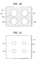
- the diaphragm 810 has four circular openings 810a, 810b, 810c, and 810d as shown in Fig. 21.
- Object light which enters a light incidence plane 800e of an objective lens 800 from the openings are projected from four lens portions 800a, 800b, 800c, and 800d of the objective lens 800 to form four object images on the image pickup plane of a solid-state image pickup element 820.
- the diaphragm 810, the light incidence plane 800e, and the image pickup plane of the solid-state image pickup element 820 are in parallel with one another.
- the light incidence plane 800e of the objective lens 800 is a plane here, the light incidence plane 800e may be formed as four spherical surfaces or four rotation-symmetry rotation-symmetry nonspherical surfaces.
- the four lens portions 800a, 800b, 800c, and 800d have circular spherical surface portions as shown in Fig. 20 showing the objective lens 800 viewed from the side where light is projected.
- An infrared radiation cutting filter having a low transmission factor with regard to the wavelength range of 670 nm and more is formed on the spherical surface portions while a light-shielding layer is formed on a plane portion 800f shown with hatching.
- the objective optical system is formed with the objective lens 800 and the diaphragm 810, while the four lens portions 800a, 800b, 800c, and 800d are the imaging system.
- Fig. 22 is a front view of the solid-state image pickup element 820.
- the solid-state image pickup element 820 is provided with four image pickup regions 820a, 820b, 820c, and 820d corresponding to the formed four object images.
- Each of the image pickup regions 820a, 820b, 820c, and 820d is sized to be 2.24 mm x 1.68 mm with the arrangement of 800 x 600 pixels having the vertical and horizontal pitch of 2.8 ⁇ m.
- the size of the whole image pickup regions is 4.78 mm x 3.36 mm, including an image pickup region separator of 0.3 mm in the middle.
- the diagonal size of each of the image pickup regions is 2.80 mm.
- image circles 851a, 851b, 851c, and 851d within which an object image is formed are circular the sizes of which are determined based on the openings of the diaphragm and the size of the spherical surface portions on the projection side of the objective lens 800.
- the image circles 851a, 851b, 851c, and 851d overlap one another.
- hatched portions 852a and 852b sandwiched between the diaphragm 810 and the objective lens 800 are optical filters formed on the light incidence plane 800e of the objective lens 800.
- the optical filters 852a, 852b, 852c, and 852d are formed in regions which completely include the diaphragm openings 810a, 810b, 810c, and 810d, respectively.
- the optical filters 852a and 852d have spectral transmission factor characteristics shown as G in Fig. 6 which mainly transmit green, the optical filter 852b has spectral transmission factor characteristics shown as R which mainly transmit red, and the optical filter 852c has spectral transmission factor characteristics shown as B which mainly transmit blue, and thus, these are primary color filters.
- the object images formed in the image circles 851a and 851d are of green light component, the object image formed in the image circle 851b is of red light component, and the object image formed in the image circle 851c is of blue light component.
- optical filters 853a, 853b, 853c, and 853d are formed on the four image pickup regions 820a, 820b, 820c, and 820d, respectively, of the solid-state image pickup element 820.
- Their spectral transmission factor characteristics are equivalent to the ones shown in Fig. 6. More specifically, the image pickup regions 820a and 820d are sensitive to green light (G), the image pickup region 820b is sensitive to red light (R), and the image pickup region 820c is sensitive to blue light (B).
- the combination of the pupil and the image pickup region is selected according to the wavelength range.
- object light which goes through the diaphragm opening 810a is mainly photoelectrically converted in the image pickup region 820a
- object light which goes through the diaphragm opening 810b is mainly photoelectrically converted in the image pickup region 820b
- object light which goes through the diaphragm opening 810c is mainly photoelectrically converted in the image pickup region 820c
- object light which goes through the diaphragm opening 810d is mainly photoelectrically converted in the image pickup region 820d.
- the image pickup regions 820a and 820d output G images
- the image pickup region 820b outputs an R image
- the image pickup region 820c outputs a B image, respectively.
- the color purity can be enhanced.
- the separator between the image pickup regions is provided for the purpose of preventing overlap of the image circles in the image pickup regions 820a and 820d, since both of them obtain G image signals.
- a color image is formed based on the photoelectric conversion output of one of the plurality of images obtained in the plurality of image pickup regions of the solid-state image pickup element 820.
- the signal processing is carried out with a G image signal including this wavelength being as the reference image signal. Since a G object image is formed both in the image pickup region 820a and in the image pickup region 820d, the number of pixels of the G object image is twice as much as that of the R object image or the B object image, and thus, a particularly high definition image can be obtained in the wavelength range having the highest luminosity factor.
- pixel shift is used where, by shifting relatively the image pickup regions 820a and 820d of the solid-state image pickup element by 1/2 pixel, the resolution is made higher with a small number of pixels.
- the amount of the shift of 1/2 pixel is set with regard to the virtual object distance 2 m.
- This pixel shift may be materialized by making the lens portion 800d of the objective lens 800 slightly offset with respect to the lens portion 800a, or may be materialized by making the image pickup region 820d of the solid-state image pickup element 820 slightly offset with respect to the image pickup region 820a.
- each of the image pickup regions is sized to be 2.24 mm ⁇ 1.68 mm, and each two of them are arranged adjacent to each other with their longer sides being in contact with each other. The two pairs are in parallel with each other with the separator of 0.3 mm therebetween. Therefore, the center-to-center distance of adjoining image pickup regions is 1.68 mm in the vertical direction and 2.54 mm in the horizontal direction.
- the distance between image pickup regions is longest with regard to the image pickup regions 820a and 820d, and with regard to the image pickup regions 820b and 820c, which are positioned obliquely with respect to each other. This longest distance is 3.045 mm in both cases.
- the YC processing circuit 230 In the YC processing circuit 230 to be described later, signal processing is carried out on the assumption that the center of an object image is the center of the image pickup region.
- the image pickup regions 820a and 820d in case of that object images with the virtual object distance 2 m are to be formed on the image pickup portion so as to keep the interval of 3.045 mm which is the same as the interval between the image pickup regions, as shown in Fig. 23, the interval between the lens portions 800a and 800d of the objective lens 800 is set to be 3.0420 mm.
- arrows 855a and 855d denote imaging systems having positive power by the lens portions 800a and 800d of the objective lens 800, respectively
- rectangles 856a and 856d denote the ranges of the image pickup regions 820a and 820d, respectively
- L801 and L802 are optical axes of the imaging systems 855a and 855d, respectively. Since the light incidence surface 800e of the objective lens 800 is a plane and the lens portions 800a and 800d which are the light projection surface are spherical surfaces, perpendiculars from the respective centers of the spheres to the light incidence plane are the optical axes.
- ⁇ Y is 3.0 ⁇ m and thus, color misalignment by this amount is caused with regard to an image at infinity. Therefore, two problems have to be considered: fluctuation in the interval between the G object images, and misalignment of the R object image and the B object image.
- the spectral luminous efficiency is high with regard to a G object image and thus the G object image can be recognizable even with slight decrease in its resolution
- the fluctuation in the interval between the G object images is-considered. If such the interval is allowable, it can be understood that the misalignment of the R object image and the B object image causes no problem.
- optical filters used for the color separation are primary color filters of red, green, and blue.
- the present invention is also applicable to a case where these filters are replaced by complementary color filters of cyan, magenta, and yellow.
- an object image having the highest luminosity factor (green) is used as a reference to describe change in the intervals between the object image having the highest luminosity factor and object images having other luminosity factors (other colors), which caused by change in the distance to the object.
- the present invention is also applicable to a case where an object image having the highest luminosity factor (green) is not used as the reference.
Landscapes
- Engineering & Computer Science (AREA)
- Multimedia (AREA)
- Signal Processing (AREA)
- Physics & Mathematics (AREA)
- Spectroscopy & Molecular Physics (AREA)
- Color Television Image Signal Generators (AREA)
- Endoscopes (AREA)
Applications Claiming Priority (2)
| Application Number | Priority Date | Filing Date | Title |
|---|---|---|---|
| JP18566199 | 1999-06-30 | ||
| JP18566199 | 1999-06-30 |
Publications (2)
| Publication Number | Publication Date |
|---|---|
| EP1067779A2 true EP1067779A2 (fr) | 2001-01-10 |
| EP1067779A3 EP1067779A3 (fr) | 2002-11-27 |
Family
ID=16174668
Family Applications (1)
| Application Number | Title | Priority Date | Filing Date |
|---|---|---|---|
| EP00305472A Withdrawn EP1067779A3 (fr) | 1999-06-30 | 2000-06-29 | Dispositif de prise de vue |
Country Status (2)
| Country | Link |
|---|---|
| US (1) | US6859229B1 (fr) |
| EP (1) | EP1067779A3 (fr) |
Cited By (10)
| Publication number | Priority date | Publication date | Assignee | Title |
|---|---|---|---|---|
| US6635941B2 (en) | 2001-03-21 | 2003-10-21 | Canon Kabushiki Kaisha | Structure of semiconductor device with improved reliability |
| FR2880958A1 (fr) * | 2005-01-19 | 2006-07-21 | Dxo Labs Sa | Procede d'amelioration de la nettete d'au moins une couleur d'une image numerique |
| US7110034B2 (en) | 2001-08-31 | 2006-09-19 | Canon Kabushiki Kaisha | Image pickup apparatus containing light adjustment portion with reflection of a portion of light onto adjacent pixels |
| WO2006095110A3 (fr) * | 2005-03-07 | 2006-11-02 | Dxo Labs | Procédé pour commander une action, notamment une modification de netteté, à partir d'une image numérique en couleurs |
| US7329856B2 (en) | 2004-08-24 | 2008-02-12 | Micron Technology, Inc. | Image sensor having integrated infrared-filtering optical device and related method |
| CN1677217B (zh) * | 2004-03-31 | 2010-08-25 | 松下电器产业株式会社 | 摄像装置及摄像用光检测装置 |
| EP2315448A1 (fr) * | 2004-01-26 | 2011-04-27 | Tessera North America, Inc. | Appareil photo mince a resolution subpixellaire |
| US8049806B2 (en) | 2004-09-27 | 2011-11-01 | Digitaloptics Corporation East | Thin camera and associated methods |
| KR101185881B1 (ko) | 2006-07-17 | 2012-09-25 | 디지털옵틱스 코포레이션 이스트 | 카메라 시스템 및 관련 방법들 |
| US8953087B2 (en) | 2004-04-08 | 2015-02-10 | Flir Systems Trading Belgium Bvba | Camera system and associated methods |
Families Citing this family (22)
| Publication number | Priority date | Publication date | Assignee | Title |
|---|---|---|---|---|
| US7834923B2 (en) * | 2003-03-13 | 2010-11-16 | Hewlett-Packard Development Company, L.P. | Apparatus and method for producing and storing multiple video streams |
| FI20031816A0 (fi) * | 2003-12-11 | 2003-12-11 | Nokia Corp | Menetelmä ja laite kuvan luomiseksi |
| US20050128509A1 (en) * | 2003-12-11 | 2005-06-16 | Timo Tokkonen | Image creating method and imaging device |
| TWI275830B (en) * | 2004-02-25 | 2007-03-11 | Synge Technology Corpation | Lens for chromatic aberration compensating |
| US7158181B2 (en) * | 2004-05-04 | 2007-01-02 | Andrew G. Cartlidge | System and methods for increasing fill-factor on pixelated sensor arrays |
| US7738026B2 (en) * | 2005-05-02 | 2010-06-15 | Andrew G. Cartlidge | Increasing fill-factor on pixelated sensors |
| US7911516B2 (en) * | 2004-09-27 | 2011-03-22 | Panasonic Corporation | Camera module and electronic apparatus provided with it |
| US7483065B2 (en) * | 2004-12-15 | 2009-01-27 | Aptina Imaging Corporation | Multi-lens imaging systems and methods using optical filters having mosaic patterns |
| WO2006068129A1 (fr) * | 2004-12-22 | 2006-06-29 | Matsushita Electric Industrial Co., Ltd. | Dispositif d’imagerie et procédé de fabrication idoine |
| US20070102622A1 (en) | 2005-07-01 | 2007-05-10 | Olsen Richard I | Apparatus for multiple camera devices and method of operating same |
| CN101533202B (zh) * | 2005-07-26 | 2011-04-13 | 松下电器产业株式会社 | 复眼方式的摄像装置 |
| US20080165257A1 (en) * | 2007-01-05 | 2008-07-10 | Micron Technology, Inc. | Configurable pixel array system and method |
| US8101903B2 (en) | 2007-01-23 | 2012-01-24 | Micron Technology, Inc. | Method, apparatus and system providing holographic layer as micro-lens and color filter array in an imager |
| US7812869B2 (en) * | 2007-05-11 | 2010-10-12 | Aptina Imaging Corporation | Configurable pixel array system and method |
| US20110141336A1 (en) * | 2009-12-11 | 2011-06-16 | Apple Inc. | Photochromatic coating for controlling lens flare |
| JP2011216701A (ja) * | 2010-03-31 | 2011-10-27 | Sony Corp | 固体撮像装置及び電子機器 |
| JP5582935B2 (ja) * | 2010-09-22 | 2014-09-03 | 富士フイルム株式会社 | 撮像モジュール |
| US20120241600A1 (en) * | 2011-03-24 | 2012-09-27 | Centera Photonics Inc. | Optical electrical module |
| US11009788B2 (en) | 2011-09-09 | 2021-05-18 | Centera Photonics Inc. | Method for manufacturing optical electrical module and substrate of an optical electrical module |
| US9581772B2 (en) | 2011-09-09 | 2017-02-28 | Centera Photonics Inc. | Optical electrical module used for optical communication |
| US9408527B2 (en) * | 2012-11-01 | 2016-08-09 | Karl Storz Imaging, Inc. | Solid state variable direction of view endoscope with rotatable wide-angle field for maximal image performance |
| US12250437B2 (en) * | 2020-04-03 | 2025-03-11 | Rockwell Collins, Inc. | Color night vision system and method |
Citations (2)
| Publication number | Priority date | Publication date | Assignee | Title |
|---|---|---|---|---|
| US3304435A (en) * | 1963-07-18 | 1967-02-14 | Donald W Norwood | Photometric device having greater response to a preferential central portion of a scene |
| US5777674A (en) * | 1994-04-11 | 1998-07-07 | Canon Kabushiki Kaisha | Four color separation optical device |
Family Cites Families (28)
| Publication number | Priority date | Publication date | Assignee | Title |
|---|---|---|---|---|
| US4028725A (en) | 1976-04-21 | 1977-06-07 | Grumman Aerospace Corporation | High-resolution vision system |
| JPS60241277A (ja) | 1984-05-15 | 1985-11-30 | Sharp Corp | 半導体装置 |
| JPS6116580A (ja) | 1984-07-03 | 1986-01-24 | Matsushita Electronics Corp | 光検知半導体装置 |
| JPS62109376A (ja) | 1985-11-08 | 1987-05-20 | Nissan Motor Co Ltd | 受光用半導体装置 |
| US4724354A (en) | 1986-05-05 | 1988-02-09 | Eol3 Company, Inc. | Image intensifier for producing a color image having a color separation filter sequentially passing visible blue light and its second order wavelengths, visible green light and its second order wavelengths, and visible red light |
| JPS6344624A (ja) | 1986-08-12 | 1988-02-25 | Fuji Photo Film Co Ltd | 液晶デバイス |
| US4873572A (en) | 1987-02-27 | 1989-10-10 | Olympus Optical Co., Ltd. | Electronic endoscope apparatus |
| JPH01150372A (ja) | 1987-12-07 | 1989-06-13 | Mitsubishi Electric Corp | フオトセンサ |
| JPH01248542A (ja) | 1988-03-29 | 1989-10-04 | Nec Corp | 固体受光装置 |
| US5262819A (en) | 1989-07-07 | 1993-11-16 | Canon Kabushiki Kaisha | Compact focus detecting device suitable for incorporation into an optical apparatus |
| JPH03286566A (ja) | 1990-04-03 | 1991-12-17 | Toshiba Corp | 固体撮像素子の製造方法 |
| GB9125954D0 (en) | 1991-12-06 | 1992-02-05 | Vlsi Vision Ltd | Electronic camera |
| US5255088A (en) * | 1992-01-29 | 1993-10-19 | Arc Machines, Inc. | System and process for video monitoring a welding operation |
| JP3203904B2 (ja) | 1993-09-10 | 2001-09-04 | キヤノン株式会社 | 撮像装置 |
| DE69426586T2 (de) * | 1993-09-23 | 2001-05-31 | Sharp K.K., Osaka | Integrierte elektrooptische Flüssigkristallvorrichtung und Verfahren zu seiner Verwendung |
| JP3397397B2 (ja) | 1993-10-22 | 2003-04-14 | キヤノン株式会社 | 撮像装置 |
| US5694165A (en) | 1993-10-22 | 1997-12-02 | Canon Kabushiki Kaisha | High definition image taking apparatus having plural image sensors |
| JP3066944B2 (ja) | 1993-12-27 | 2000-07-17 | キヤノン株式会社 | 光電変換装置、その駆動方法及びそれを有するシステム |
| JPH0846877A (ja) * | 1994-04-08 | 1996-02-16 | Hewlett Packard Co <Hp> | イメージ測定装置 |
| US5940126A (en) | 1994-10-25 | 1999-08-17 | Kabushiki Kaisha Toshiba | Multiple image video camera apparatus |
| US6560018B1 (en) | 1994-10-27 | 2003-05-06 | Massachusetts Institute Of Technology | Illumination system for transmissive light valve displays |
| US6388709B1 (en) | 1995-04-21 | 2002-05-14 | Canon Kabushiki Kaisha | Image sensing apparatus with optical modulation elements having transmission characteristics controllable by pixel |
| JP3498775B2 (ja) | 1995-05-31 | 2004-02-16 | ソニー株式会社 | 撮像装置 |
| US6122009A (en) | 1995-05-31 | 2000-09-19 | Sony Corporation | Image pickup apparatus fabrication method thereof image pickup adaptor apparatus signal processing apparatus signal processing method thereof information processing apparatus and information processing method |
| JP3713321B2 (ja) | 1995-12-19 | 2005-11-09 | オリンパス株式会社 | カラー画像記録再生システム及び画像カラー画像記録再生方法 |
| JPH09294269A (ja) | 1996-04-25 | 1997-11-11 | Kureha Chem Ind Co Ltd | カラー撮像装置 |
| US6137535A (en) | 1996-11-04 | 2000-10-24 | Eastman Kodak Company | Compact digital camera with segmented fields of view |
| JP3290091B2 (ja) * | 1997-03-31 | 2002-06-10 | シャープ株式会社 | 投影型画像表示装置 |
-
2000
- 2000-06-28 US US09/604,745 patent/US6859229B1/en not_active Expired - Lifetime
- 2000-06-29 EP EP00305472A patent/EP1067779A3/fr not_active Withdrawn
Patent Citations (2)
| Publication number | Priority date | Publication date | Assignee | Title |
|---|---|---|---|---|
| US3304435A (en) * | 1963-07-18 | 1967-02-14 | Donald W Norwood | Photometric device having greater response to a preferential central portion of a scene |
| US5777674A (en) * | 1994-04-11 | 1998-07-07 | Canon Kabushiki Kaisha | Four color separation optical device |
Cited By (15)
| Publication number | Priority date | Publication date | Assignee | Title |
|---|---|---|---|---|
| EP1244151A3 (fr) * | 2001-03-21 | 2007-10-10 | Canon Kabushiki Kaisha | Dispositif semi-conducteur et son procédé de fabrication |
| US6893941B2 (en) | 2001-03-21 | 2005-05-17 | Canon Kabushiki Kaisha | Semiconductor device and its manufacture method |
| US6635941B2 (en) | 2001-03-21 | 2003-10-21 | Canon Kabushiki Kaisha | Structure of semiconductor device with improved reliability |
| US7110034B2 (en) | 2001-08-31 | 2006-09-19 | Canon Kabushiki Kaisha | Image pickup apparatus containing light adjustment portion with reflection of a portion of light onto adjacent pixels |
| EP2315448A1 (fr) * | 2004-01-26 | 2011-04-27 | Tessera North America, Inc. | Appareil photo mince a resolution subpixellaire |
| CN1677217B (zh) * | 2004-03-31 | 2010-08-25 | 松下电器产业株式会社 | 摄像装置及摄像用光检测装置 |
| US8953087B2 (en) | 2004-04-08 | 2015-02-10 | Flir Systems Trading Belgium Bvba | Camera system and associated methods |
| US7329856B2 (en) | 2004-08-24 | 2008-02-12 | Micron Technology, Inc. | Image sensor having integrated infrared-filtering optical device and related method |
| DE102005016564B4 (de) * | 2004-08-24 | 2011-06-22 | Aptina Imaging Corp., Cayman Islands | Bildsensor mit integrierter elektrischer optischer Vorrichtung |
| US8049806B2 (en) | 2004-09-27 | 2011-11-01 | Digitaloptics Corporation East | Thin camera and associated methods |
| FR2880958A1 (fr) * | 2005-01-19 | 2006-07-21 | Dxo Labs Sa | Procede d'amelioration de la nettete d'au moins une couleur d'une image numerique |
| WO2006095110A3 (fr) * | 2005-03-07 | 2006-11-02 | Dxo Labs | Procédé pour commander une action, notamment une modification de netteté, à partir d'une image numérique en couleurs |
| US7920172B2 (en) | 2005-03-07 | 2011-04-05 | Dxo Labs | Method of controlling an action, such as a sharpness modification, using a colour digital image |
| US8212889B2 (en) | 2005-03-07 | 2012-07-03 | Dxo Labs | Method for activating a function, namely an alteration of sharpness, using a colour digital image |
| KR101185881B1 (ko) | 2006-07-17 | 2012-09-25 | 디지털옵틱스 코포레이션 이스트 | 카메라 시스템 및 관련 방법들 |
Also Published As
| Publication number | Publication date |
|---|---|
| US6859229B1 (en) | 2005-02-22 |
| EP1067779A3 (fr) | 2002-11-27 |
Similar Documents
| Publication | Publication Date | Title |
|---|---|---|
| US6859229B1 (en) | Image pickup apparatus | |
| US6882368B1 (en) | Image pickup apparatus | |
| US6833873B1 (en) | Image pickup apparatus | |
| US20020089596A1 (en) | Image sensing apparatus | |
| US6980248B1 (en) | Image pickup apparatus | |
| US7847843B2 (en) | Image sensing apparatus and its control method, control program, and storage medium for correcting position deviation of images | |
| US7367537B2 (en) | Color-image pickup device in which an R picture signal is relatively enhanced with distance from center of light-reception area | |
| US7110034B2 (en) | Image pickup apparatus containing light adjustment portion with reflection of a portion of light onto adjacent pixels | |
| KR100553056B1 (ko) | 촬상장치 | |
| US7112779B2 (en) | Optical apparatus and beam splitter | |
| JP2002135796A (ja) | 撮像装置 | |
| JP3703424B2 (ja) | 撮像装置及びその制御方法及び制御プログラム及び記憶媒体 | |
| KR20030069885A (ko) | 촬상장치 | |
| US6885404B1 (en) | Image pickup apparatus | |
| EP1653257B1 (fr) | Appareil de capture d'images | |
| EP0618470A1 (fr) | Système optique de prise de vues | |
| JP3397758B2 (ja) | 撮像装置 | |
| JP3397754B2 (ja) | 撮像装置 | |
| JP4083355B2 (ja) | 撮像装置 | |
| JP3397755B2 (ja) | 撮像装置 | |
| US20070052833A1 (en) | Variable magnification optical system and image-taking apparatus | |
| JP2002158913A (ja) | 撮像装置及び撮像方法 | |
| JP3397757B2 (ja) | 撮像装置 | |
| JP3397756B2 (ja) | 撮像装置 | |
| US7474349B2 (en) | Image-taking apparatus |
Legal Events
| Date | Code | Title | Description |
|---|---|---|---|
| PUAI | Public reference made under article 153(3) epc to a published international application that has entered the european phase |
Free format text: ORIGINAL CODE: 0009012 |
|
| AK | Designated contracting states |
Kind code of ref document: A2 Designated state(s): AT BE CH CY DE DK ES FI FR GB GR IE IT LI LU MC NL PT SE |
|
| AX | Request for extension of the european patent |
Free format text: AL;LT;LV;MK;RO;SI |
|
| PUAL | Search report despatched |
Free format text: ORIGINAL CODE: 0009013 |
|
| AK | Designated contracting states |
Kind code of ref document: A3 Designated state(s): AT BE CH CY DE DK ES FI FR GB GR IE IT LI LU MC NL PT SE |
|
| AX | Request for extension of the european patent |
Free format text: AL;LT;LV;MK;RO;SI |
|
| 17P | Request for examination filed |
Effective date: 20030411 |
|
| AKX | Designation fees paid |
Designated state(s): DE FR GB |
|
| 17Q | First examination report despatched |
Effective date: 20040311 |
|
| STAA | Information on the status of an ep patent application or granted ep patent |
Free format text: STATUS: THE APPLICATION IS DEEMED TO BE WITHDRAWN |
|
| 18D | Application deemed to be withdrawn |
Effective date: 20060302 |