EP1073120A2 - Procédé de fabrication d'une mémoire NROM - Google Patents
Procédé de fabrication d'une mémoire NROM Download PDFInfo
- Publication number
- EP1073120A2 EP1073120A2 EP00305940A EP00305940A EP1073120A2 EP 1073120 A2 EP1073120 A2 EP 1073120A2 EP 00305940 A EP00305940 A EP 00305940A EP 00305940 A EP00305940 A EP 00305940A EP 1073120 A2 EP1073120 A2 EP 1073120A2
- Authority
- EP
- European Patent Office
- Prior art keywords
- layer
- oxide
- nitride
- ono
- chip
- Prior art date
- Legal status (The legal status is an assumption and is not a legal conclusion. Google has not performed a legal analysis and makes no representation as to the accuracy of the status listed.)
- Withdrawn
Links
Images

Classifications
-
- H—ELECTRICITY
- H10—SEMICONDUCTOR DEVICES; ELECTRIC SOLID-STATE DEVICES NOT OTHERWISE PROVIDED FOR
- H10B—ELECTRONIC MEMORY DEVICES
- H10B43/00—EEPROM devices comprising charge-trapping gate insulators
- H10B43/30—EEPROM devices comprising charge-trapping gate insulators characterised by the memory core region
-
- H—ELECTRICITY
- H10—SEMICONDUCTOR DEVICES; ELECTRIC SOLID-STATE DEVICES NOT OTHERWISE PROVIDED FOR
- H10B—ELECTRONIC MEMORY DEVICES
- H10B41/00—Electrically erasable-and-programmable ROM [EEPROM] devices comprising floating gates
-
- H—ELECTRICITY
- H10—SEMICONDUCTOR DEVICES; ELECTRIC SOLID-STATE DEVICES NOT OTHERWISE PROVIDED FOR
- H10B—ELECTRONIC MEMORY DEVICES
- H10B69/00—Erasable-and-programmable ROM [EPROM] devices not provided for in groups H10B41/00 - H10B63/00, e.g. ultraviolet erasable-and-programmable ROM [UVEPROM] devices
-
- H—ELECTRICITY
- H10—SEMICONDUCTOR DEVICES; ELECTRIC SOLID-STATE DEVICES NOT OTHERWISE PROVIDED FOR
- H10D—INORGANIC ELECTRIC SEMICONDUCTOR DEVICES
- H10D30/00—Field-effect transistors [FET]
- H10D30/60—Insulated-gate field-effect transistors [IGFET]
- H10D30/69—IGFETs having charge trapping gate insulators, e.g. MNOS transistors
-
- H—ELECTRICITY
- H10—SEMICONDUCTOR DEVICES; ELECTRIC SOLID-STATE DEVICES NOT OTHERWISE PROVIDED FOR
- H10D—INORGANIC ELECTRIC SEMICONDUCTOR DEVICES
- H10D64/00—Electrodes of devices having potential barriers
- H10D64/01—Manufacture or treatment
- H10D64/031—Manufacture or treatment of data-storage electrodes
- H10D64/037—Manufacture or treatment of data-storage electrodes comprising charge-trapping insulators
-
- H—ELECTRICITY
- H10—SEMICONDUCTOR DEVICES; ELECTRIC SOLID-STATE DEVICES NOT OTHERWISE PROVIDED FOR
- H10P—GENERIC PROCESSES OR APPARATUS FOR THE MANUFACTURE OR TREATMENT OF DEVICES COVERED BY CLASS H10
- H10P14/00—Formation of materials, e.g. in the shape of layers or pillars
- H10P14/60—Formation of materials, e.g. in the shape of layers or pillars of insulating materials
- H10P14/61—Formation of materials, e.g. in the shape of layers or pillars of insulating materials using masks
-
- H—ELECTRICITY
- H10—SEMICONDUCTOR DEVICES; ELECTRIC SOLID-STATE DEVICES NOT OTHERWISE PROVIDED FOR
- H10P—GENERIC PROCESSES OR APPARATUS FOR THE MANUFACTURE OR TREATMENT OF DEVICES COVERED BY CLASS H10
- H10P14/00—Formation of materials, e.g. in the shape of layers or pillars
- H10P14/60—Formation of materials, e.g. in the shape of layers or pillars of insulating materials
- H10P14/63—Formation of materials, e.g. in the shape of layers or pillars of insulating materials characterised by the formation processes
- H10P14/6326—Deposition processes
- H10P14/6328—Deposition from the gas or vapour phase
- H10P14/6334—Deposition from the gas or vapour phase using decomposition or reaction of gaseous or vapour phase compounds, i.e. chemical vapour deposition
-
- H—ELECTRICITY
- H10—SEMICONDUCTOR DEVICES; ELECTRIC SOLID-STATE DEVICES NOT OTHERWISE PROVIDED FOR
- H10P—GENERIC PROCESSES OR APPARATUS FOR THE MANUFACTURE OR TREATMENT OF DEVICES COVERED BY CLASS H10
- H10P14/00—Formation of materials, e.g. in the shape of layers or pillars
- H10P14/60—Formation of materials, e.g. in the shape of layers or pillars of insulating materials
- H10P14/66—Formation of materials, e.g. in the shape of layers or pillars of insulating materials characterised by the type of materials
- H10P14/662—Laminate layers, e.g. stacks of alternating high-k metal oxides
-
- Y—GENERAL TAGGING OF NEW TECHNOLOGICAL DEVELOPMENTS; GENERAL TAGGING OF CROSS-SECTIONAL TECHNOLOGIES SPANNING OVER SEVERAL SECTIONS OF THE IPC; TECHNICAL SUBJECTS COVERED BY FORMER USPC CROSS-REFERENCE ART COLLECTIONS [XRACs] AND DIGESTS
- Y10—TECHNICAL SUBJECTS COVERED BY FORMER USPC
- Y10S—TECHNICAL SUBJECTS COVERED BY FORMER USPC CROSS-REFERENCE ART COLLECTIONS [XRACs] AND DIGESTS
- Y10S438/00—Semiconductor device manufacturing: process
- Y10S438/954—Making oxide-nitride-oxide device
Definitions
- the present invention relates generally to methods of fabrication of nitride read only memory (NROM) cells and arrays.
- NROM nitride read only memory
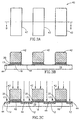
- Fig. 1 illustrates a typical prior art NROM cell.
- This cell includes a substrate 10 in which are implanted a source 12 and a drain 14 and on top of which lies an oxide-nitride-oxide (ONO) structure 16 having a layer of nitride 17 sandwiched between two oxide layers 18 and 20.
- ONO oxide-nitride-oxide
- Nitride section 17 provides the charge retention mechanism for programming the memory cell. Specifically, when programming voltages are provided to source 12, drain 14 and gate conductor 22, electrons flow towards drain 14. According to the hot electron injection phenomenon, some hot electrons penetrate through the lower section of silicon oxide 18, especially if section 18 is thin, and are then collected in nitride section 17. As is known in the art, nitride section 17 retains the received charge, labeled 24, in a concentrated area adjacent drain 14. Concentrated charge 24 significantly raises the threshold of the portion of the channel of the memory cell under charge 24 to be higher than the threshold of the remaining portion of the channel 15.
- the raised threshold of the cell does not permit the cell to be placed into a conductive state during reading of the cell. If concentrated charge 24 is not present, the read voltage on gate conductor 22 can overcome the much lower threshold and accordingly, channel 15 becomes inverted and hence, conductive.
- the threshold voltage Vth of NROM cells is generally very sensitive to the voltages V drain and Vgate provided on the drain 14 and on the gate 22, respectively. Furthermore, US 5,768,192 selects the voltages Vdrain and Vgate in order to ensure that the charge trapped in a portion of the nitride layer 17 remains localized in that portion.
- Read only memory cells including a nitride layer in the gate dielectric (NROM) are described, inter alia, in US patents 5,168,334 to Mitchell et al. and 4,173,766 to Hayes.
- Mitchell et al. describe two processes to produce the NROM cells.
- bit lines are first created in the substrate, after which the surface is oxidized. Following the oxidation, the ONO layers are added over the entire array. Polysilicon word lines are then deposited in rows over the ONO layers.
- an oxide layer typically under high temperature
- the already present bit lines will diffuse to the side, an undesirable occurrence which limits the extent to which the cell size can be shrunk.
- the ONO layers are formed over the entire array first, on top of which conductive blocks of polysilicon are formed.
- the bit lines are implanted between the blocks of polysilicon after which the ONO layers are etched away from on top of the bit lines.
- Planarized oxide is then deposited between the polysilicon blocks after which polysilicon word lines are deposited.
- Mitchell et al. utilize a planarized oxide since such can be deposited rather than grown.
- Mitchell et al. cannot grow an oxide over the bit lines since such an oxidation operation would also grow oxide over the polysilicon blocks and the latter must be left with a very clean surface in order to connect with the polysilicon word lines.
- planarized oxide is not a clean oxide nor does it seal around the edges of the ONO sections.
- the planarized oxide adds complexity and cost to the process.
- Hayes et al. describe an NROM cell having only an oxide-nitride (ON) layer.
- the cells in the array are created by forming layers of oxide, nitride and polysilicon (the latter to produce the gate) one after another and then patterning and etching these layers to form the cells.
- the uncapped nitride in each cell does not hold charge well in both the vertical and lateral directions. Due to hole and hot electron conduction within the nitride, the charge to be stored will flow vertically towards the gate covering it unless the nitride is thick and will flow laterally in the nitride in response to lateral electric fields.
- the present invention provides a method of fabricating an oxide-nitride-oxide (ONO) layer as set out Claims 1, 2, 3 and 6, a method for improving the charge retention in a nitride layer of a memory chip as set out in Claim 4 or Claim 5, and a method of fabricating a nitride read only memory (NROM) chip as set out in Claim 7, Claim 12, Claim 16 or Claim 17 of the accompanying claims.
- OEO oxide-nitride-oxide
- a method of fabricating an NROM chip includes the steps of a) creating an oxide-nitride-oxide (ONO) layer on a substrate, b) within a memory portion of the chip, etching the ONO layer into columns and leaving a portion of the bottom oxide in the areas between the columns, c) implanting bit lines between the columns, d) forming bit line oxides on top of the bit lines and e) forming rows of polysilicon or polysilicide perpendicular to and on top of the bit line oxides and ONO columns.
- ONO oxide-nitride-oxide
- the threshold voltage level of the entire chip can be adjusted after which the ONO layer is removed from at least most of a periphery portion of the chip.
- the threshold voltage level of the unmasked portions of the chip is adjusted, after which the ONO layer is removed from the unmasked portions of the chip.
- top oxide layer can be generated via deposition, oxidation or a combination of both.
- a method of fabricating an oxide-nitride-oxide (ONO) layer in a memory cell to retain charge in the nitride layer includes the steps of forming a bottom oxide layer on a substrate, depositing a nitride layer and oxidizing a top oxide layer, thereby causing oxygen to be introduced into the nitride layer.
- ONO oxide-nitride-oxide
- the method includes the steps of forming a bottom oxide layer on a substrate, depositing a nitride layer, oxidizing a portion of a top oxide layer thereby causing oxygen to be introduced into the nitride layer and depositing a remaining portion of the top oxide layer, thereby assisting in controlling the amount of oxygen introduced into the nitride layer.
- the method includes the steps of forming a bottom oxide layer on a substrate, depositing a nitride layer, depositing a portion of a top oxide layer and oxidizing a remaining portion of the top oxide layer, thereby causing oxygen to be introduced into the nitride layer.
- a method for improving the charge retention in a nitride layer of a memory chip includes the steps of depositing a nitride layer and introducing oxygen into the nitride layer.
- the method includes the steps of depositing a nitride layer, controlling the thickness of the deposited nitride layer and introducing oxygen into the nitride layer.
- the method includes the steps of forming a bottom oxide layer on a substrate, depositing a nitride layer at a thickness approximate to the final thickness after fabrication, depositing a portion of a top oxide layer and oxidizing a remaining portion of the top oxide layer, thereby assisting in controlling the introduction of oxygen into the nitride layer.
- Figs. 2, 3A, 3B, 3C, 4, 5, 6A and 6B illustrate the NROM fabrication method of the present invention. Similar reference numerals herein refer to similar elements. It is noted that the present invention covers the fabrication of the entire chip, which includes the NROM memory array portion and the complementary metal oxide semiconductor (CMOS) periphery devices.
- CMOS complementary metal oxide semiconductor
- etching a layer which includes placing photoresist on the layer, placing a mask on the photoresist, etching wherever the mask is not and removing the photoresist, will not be detailed.
- CMOS complementary metal oxide semiconductor
- a screen oxide layer is then grown (not shown) on substrate 10 after which it is removed, typically with a wet etch thereby to remove any residual nitride at the edge of the field.
- a typical thickness of the screen oxide layer is 200 - 400 ⁇
- Substrate 10 is then overlaid with an ONO layer.
- a bottom oxide layer 30 is grown over substrate 10 typically to a thickness of between 50 ⁇ and 150 ⁇ in a low temperature oxidation operation.
- a typical oxidation temperature is about 800°C but it can vary between 750 - 1000°C.
- a preferred thickness of the bottom oxide layer 30 is 80 ⁇ .
- a nitride layer 32 is then deposited over bottom oxide layer 30 to a thickness of between 20 ⁇ and 150 ⁇ where a preferred thickness is as thin as possible, such as 10 ⁇ - 50 ⁇ . Applicant notes that a thin layer of the nitride prohibits lateral movement of the charge retained within the nitride, and hence, it is beneficial to control the thickness of nitride layer 32.
- Top oxide 34 is then produced either through oxidation of the nitride (i.e. growing of the oxide), or by deposition or by a combination thereof. It is noted that top oxide 34 consumes nitride during oxidation, where typically half of the oxide thickness comes from the consumed nitride. Thus, if it is desired to have a top oxide which is 100 ⁇ thick, the nitride layer 32 should be at least 50 ⁇ thicker than the final desired nitride thickness, with this extra nitride being for consumption in the formation of the top oxide layer.
- nitride layer 32 is transformed into nitride section 17, which provides the charge retention mechanism for the memory cell.
- Nitride particularly due to its structure, traps the electrons, which are introduced into nitride section 17.
- Oxygen however, is a better insulator than nitride and helps to minimize the lateral movement of electrons in nitride layer 32. It is thus an important element for effective retention of the charge. It is therefore noted that one of the factors effecting the quality of retention ability of nitride section 17 is the concentration of oxygen within nitride layer 32.
- the oxygen concentration is defined as the percentage of oxygen atoms relative to the nitride atoms, irrespective of the type of molecule in which the oxygen atoms are found. The concentration can range from a low of 10% to a high of 80%.
- nitride layer 32 absorbs too much oxygen and ceases to act as a barrier for oxygen diffusion.
- the oxygen introduced into the oxygen rich nitride layer 32 reaches the silicone oxide layer 18, and become SIO 2 .
- nitride layer 32 in order to produce a nitride section 17 with maximum retention qualities, it is desirable to make nitride layer 32 as thin as possible, with the maximum oxygen concentration, without inducing a run-away situation. Consequently, it is critical to control the fabrication of the ONO structure, and specifically, the manner in which the top oxide 34 is produced.
- the top oxide is typically of a thickness of between 50 ⁇ and 150 ⁇ . Three alternative operations for creating a top oxide 34 of 100 ⁇ are described hereinbelow.
- the first method involves depositing nitride layer 32 of approximately 150-160 ⁇ , growing 120 - 130 ⁇ of top oxide 34, (which includes consuming 60 - 65 ⁇ of nitride layer 32) and removing 20 - 30 ⁇ of oxide layer 34 during cleaning. Since a large portion of nitride layer 32 is consumed, it is difficult to control the amount of oxygen introduced into nitride layer 32. Thus, in order to avoid a possibility of run-away conditions in the nitride layer, it is essential to "leave" a thicker nitride layer. This alternative produces a thicker nitride layer; however it provides for high introduction of oxygen into the nitride and is a simple process to perform.
- the second method involves depositing nitride layer 32 at a thickness of approximately 60 ⁇ , growing a thin layer of oxide layer 34 (approximately 40 ⁇ ) while consuming about 20 ⁇ of nitride, depositing 80-90 ⁇ and removing 20-30 ⁇ during cleaning. Since depositing oxide is a quicker process than growing oxide, this alternative is quicker than the first alternative and it offers marginally better control over the amount of oxygen introduced into nitride layer 32
- the third method involves depositing nitride layer 32 at a thickness close to the preferred final thickness, such as 20 ⁇ , depositing 100 - 110 ⁇ of oxide, growing 2 - 5 ⁇ of oxide and removing 20 - 30 ⁇ of oxide during cleaning.
- the deposited layer acts as a barrier between the growing oxide and nitride layer 32.
- the oxygen is introduced slowly into nitride layer 32.
- This alternative is slower than the previous alternatives; however, it provides a thin nitride layer and a more controlled manner for regulating the introduction of oxygen into the nitride layer.
- the process by which the nitride and top oxide layers are generated depends on the ability of the manufacturing facility to control the thickness and composition of the layers of the ONO structure.
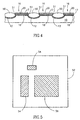
- the next step involves depositing a bit line mask 40 (typically photoresist 42 patterned in a well known manner), whose layout within the memory array portion of the chip is shown in Fig. 3A, to create the bit lines, forming lines of sources and lines of drains.
- Fig. 3B illustrates a portion of the resultant chip within the memory array portion with the photoresist 42 patterned.
- Fig. 3B is a side view (similar to Fig. 2) with the columns 42 of the bit line mask in place. Photoresist columns 42 define the areas where the bit lines are not to be implanted (i.e. the locations of the channels 15 (Fig. 1)).
- the top oxide and nitride layers 32 and 34 are etched away from the areas between columns 42.
- the etch operation is typically a dry etch which might also etch a portion 44 of bottom oxide layer 30 which is between columns 42, leaving portion 44 with a predetermined thickness, such as 50 ⁇
- the etch operation produces oxide sections 18 and 20 and nitride section 17 under each column 42.
- bit lines 12 are implanted (Fig. 3C) in the areas between columns 42.
- a typical implant might be 2 - 4x10 15 /cm2 of Arsenic at 50Kev. It will be appreciated that this is a self-aligned implant in which the bit lines are self-aligned to the ONO structures.
- bit line oxides 50 (Fig. 4) are then thermally grown over the bit lines 12 in an oxidation operation.
- side oxides 51 typically of 30 ⁇ , are grown along the sides of nitride layers 17 to improve data retention within the nitride layers.
- the oxidation typically occurs in the range of 800°C to 950°C but preferably at the lower side of this range to minimize the diffusion of the bit line impurity while maximizing the thickness of the thermal oxide. This lowers the bit line capacitance.
- the oxidation temperature also activates the implanted bit line impurities.
- the typical oxidation process is a low temperature oxidation of about 800°C which, on a P- substrate, normally is continued for a time sufficient to grow the equivalent of 100 ⁇ of thermal oxide.
- top oxide sections 20 will not significantly increase in thickness during the bit line oxidation due to the close presence of nitride sections 18 while oxide layer 44 over the bit lines 12 will increase significantly due to the presence of Arsenic in the bit lines 12.
- the result is that the bit line oxides 50 are typically very thick, such as 500 ⁇ thick, thereby lowering the bit line capacitance.
- bit line oxides 50 separates the creation of bottom oxide sections 18 (and thus, of the entire ONO structure 16) from the creation of bit line oxides 50.
- Bottom oxide sections 18 are created over the entire array as part of creating the ONO structures.
- Bit line oxides 50 are created during the bit line oxidation operation and this oxidation does not significantly affect the oxide layers in the ONO structures.
- bit line oxides 50 are self-aligned to the ONO structures and, since the oxidation operation is at a relatively low temperature, bit lines 12 do not significantly diffuse into substrate 10 during the oxidation operation.
- the ONO layers have been laid down on the entire chip and thus, are present in the periphery.
- the ONO layers can be utilized as thick gate oxides in the portions of the periphery where thicker oxides are needed.
- the present invention provides one gate dielectric using the ONO layers and the second, thinner gate dielectric can be produced in a separate gate oxide production step.
- a single mask 52 can be utilized to mark both the locations 54 of the thick gate oxides as well as to protect the memory array (area 56) while etching and oxidizing the periphery.
- Mask 52 can be utilized in one of two alternative ways.
- a threshold level adjustment implant for the peripheral transistors is performed after mask 52 is laid down and patterned. This provides the periphery with a threshold level different from that of the memory array area 56.
- the threshold level adjustment implant is performed on the entire chip prior to laying down mask 52. In this embodiment, mask 52 serves only to mark the locations where the ONO layers are to be removed.
- the threshold voltage level adjustment is performed. This procedure involves implanting boron through the ONO layers into the portions of the periphery of the chip not covered by mask 52. Typically, there are two adjustment steps, one each for the n-channel and p-channel transistors. It will be appreciated that, in accordance with a preferred embodiment of the present invention, the adjustment implant is performed through the ONO layers since they are not yet capped and thus, do not block the implant operation. It will further be appreciated that, for the threshold adjustment procedure, the to-be-removed ONO layers act as a sacrificial oxide (e.g. an oxide grown for an implant operation and immediately thereafter removed).
- a sacrificial oxide e.g. an oxide grown for an implant operation and immediately thereafter removed.
- the ONO layers on the unmasked portions of the chip are removed. Initially, a dry oxide etch is utilized to remove top oxide 34 and nitride 32 layers after which a wet etch is utilized to remove bottom oxide layer 30. Following removal of mask 52, a gate oxide (not shown) of typically 100 - 150 ⁇ is thermally grown over the entire chip. Due to the presence of nitride in the memory array, the gate oxide step does not significantly affect the thickness of top oxide 20. However, this step creates gate oxides for the transistors in the periphery.
- the gate oxide thickness is thus independent of the thicknesses of the bit line oxide 50 and top oxide 20.
- mask 52 is laid down after the gate and threshold voltage level adjustment procedure is performed.
- the memory array portion of the chip also receives threshold level adjustments.
- the ONO layers on the unmasked portions of the chip are removed, as described hereinabove.
- the ONO layers act as a sacrificial oxide, eliminating the necessity for the additional sacrificial oxide operations.
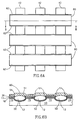
- a polysilicon layer which will create word lines for the memory array portion and will create gates for the periphery transistors, is laid down over the chip.
- a low resistive suicide as is known in the art, can be deposited over the polysilicon layer in order to reduce its resistivity. This creates a "polysilicide" layer.
- a typical total thickness of the polysilicide might be 0.3 - 0.4 ⁇ m.
- the polysilicide or polysilicon layer is then etched using a mask into word lines 60 within the memory array. Typically the word line etch also etches at least the top oxide 20 and the nitride 17 from between the word lines 60. This improves the charge retention of the memory cells by isolating the nitride layers 17 of each transistor.
- Fig. 6B illustrates one row of the resultant memory array in side view.
- the polysilicide or polysilicon layer 60 lies on top of the ONO structures 16 (Fig. 4), thereby forming the gates 22 (Fig. 1) of the NROM cells.
- Bit line oxides 50 are thick enough to isolate neighboring ONO structures 16.
- the memory chip is then finished in the standard ways, including a side wall oxidation step (typically a self-aligned step), a lightly doped drain (Ldd) implant procedure into the CMOS periphery only and a spacer deposition.
- Fig. 6A illustrates the location of the spacers 62 as being along the sidewalls of the polysilicon word lines 60.
- the Ldd typically requires separate masks for the n-channel and p-channel periphery transistors.
- the thicknesses of the various elements of the NROM cell are generally independent of each other.
- the thicknesses of the bottom oxide, nitride and top oxide layers are typically selected as a function of the desired operation of the memory array
- the bit line oxide is independent of the thickness of bottom oxide ONO structure
- the gate oxide of the periphery is independent of the other two oxide (i.e., the bit line oxide and the bottom ONO oxide) thicknesses.
Landscapes
- Non-Volatile Memory (AREA)
- Semiconductor Memories (AREA)
Applications Claiming Priority (2)
| Application Number | Priority Date | Filing Date | Title |
|---|---|---|---|
| US09/365,369 US6297096B1 (en) | 1997-06-11 | 1999-07-30 | NROM fabrication method |
| US365369 | 2003-02-11 |
Publications (2)
| Publication Number | Publication Date |
|---|---|
| EP1073120A2 true EP1073120A2 (fr) | 2001-01-31 |
| EP1073120A3 EP1073120A3 (fr) | 2001-03-07 |
Family
ID=23438603
Family Applications (1)
| Application Number | Title | Priority Date | Filing Date |
|---|---|---|---|
| EP00305940A Withdrawn EP1073120A3 (fr) | 1999-07-30 | 2000-07-13 | Procédé de fabrication d'une mémoire NROM |
Country Status (3)
| Country | Link |
|---|---|
| US (5) | US6297096B1 (fr) |
| EP (1) | EP1073120A3 (fr) |
| JP (1) | JP2001077220A (fr) |
Cited By (26)
| Publication number | Priority date | Publication date | Assignee | Title |
|---|---|---|---|---|
| US6458642B1 (en) * | 2001-10-29 | 2002-10-01 | Macronix International Co., Ltd. | Method of fabricating a sonos device |
| US6490204B2 (en) | 2000-05-04 | 2002-12-03 | Saifun Semiconductors Ltd. | Programming and erasing methods for a reference cell of an NROM array |
| WO2002080235A3 (fr) * | 2001-03-28 | 2003-03-20 | Atmel Corp | Procede de fabrication d'un dielectrique interpoly a capacite elevee |
| US6566699B2 (en) | 1997-07-30 | 2003-05-20 | Saifun Semiconductors Ltd. | Non-volatile electrically erasable and programmable semiconductor memory cell utilizing asymmetrical charge trapping |
| US6584017B2 (en) | 2001-04-05 | 2003-06-24 | Saifun Semiconductors Ltd. | Method for programming a reference cell |
| US6583007B1 (en) | 2001-12-20 | 2003-06-24 | Saifun Semiconductors Ltd. | Reducing secondary injection effects |
| US6614692B2 (en) | 2001-01-18 | 2003-09-02 | Saifun Semiconductors Ltd. | EEPROM array and method for operation thereof |
| US6633499B1 (en) | 1997-12-12 | 2003-10-14 | Saifun Semiconductors Ltd. | Method for reducing voltage drops in symmetric array architectures |
| US6633496B2 (en) | 1997-12-12 | 2003-10-14 | Saifun Semiconductors Ltd. | Symmetric architecture for memory cells having widely spread metal bit lines |
| US6636440B2 (en) | 2001-04-25 | 2003-10-21 | Saifun Semiconductors Ltd. | Method for operation of an EEPROM array, including refresh thereof |
| US6643181B2 (en) | 2001-10-24 | 2003-11-04 | Saifun Semiconductors Ltd. | Method for erasing a memory cell |
| US6677805B2 (en) | 2001-04-05 | 2004-01-13 | Saifun Semiconductors Ltd. | Charge pump stage with body effect minimization |
| US6803279B2 (en) | 1997-06-11 | 2004-10-12 | Saifun Semiconductors Ltd. | NROM fabrication method |
| US6826107B2 (en) | 2002-08-01 | 2004-11-30 | Saifun Semiconductors Ltd. | High voltage insertion in flash memory cards |
| US6829172B2 (en) | 2000-05-04 | 2004-12-07 | Saifun Semiconductors Ltd. | Programming of nonvolatile memory cells |
| US6828625B2 (en) | 2001-11-19 | 2004-12-07 | Saifun Semiconductors Ltd. | Protective layer in memory device and method therefor |
| DE10324550A1 (de) * | 2003-05-30 | 2004-12-30 | Infineon Technologies Ag | Herstellungsverfahren für eine NROM-Halbleiterspeichervorrichtung und entsprechende NROM-Halbleiterspeichervorrichtung |
| US6885585B2 (en) | 2001-12-20 | 2005-04-26 | Saifun Semiconductors Ltd. | NROM NOR array |
| US6897522B2 (en) | 2001-10-31 | 2005-05-24 | Sandisk Corporation | Multi-state non-volatile integrated circuit memory systems that employ dielectric storage elements |
| US6925007B2 (en) | 2001-10-31 | 2005-08-02 | Sandisk Corporation | Multi-state non-volatile integrated circuit memory systems that employ dielectric storage elements |
| US6928001B2 (en) | 2000-12-07 | 2005-08-09 | Saifun Semiconductors Ltd. | Programming and erasing methods for a non-volatile memory cell |
| SG114617A1 (en) * | 2002-06-14 | 2005-09-28 | Infineon Technologies Flash Gm | Integrated memory circuit and method of forming an integrated memory circuit |
| US7116577B2 (en) | 1997-08-01 | 2006-10-03 | Saifun Semiconductors Ltd | Two bit non-volatile electrically erasable and programmable semiconductor memory cell utilizing asymmetrical charge trapping |
| CN100438037C (zh) * | 2001-11-07 | 2008-11-26 | 旺宏电子股份有限公司 | 多阶nrom的存储单元及其操作方法 |
| US7535765B2 (en) | 2004-12-09 | 2009-05-19 | Saifun Semiconductors Ltd. | Non-volatile memory device and method for reading cells |
| US8569824B2 (en) | 2008-01-30 | 2013-10-29 | Panasonic Corporation | Semiconductor device and fabrication method for the same |
Families Citing this family (119)
| Publication number | Priority date | Publication date | Assignee | Title |
|---|---|---|---|---|
| US6430077B1 (en) | 1997-12-12 | 2002-08-06 | Saifun Semiconductors Ltd. | Method for regulating read voltage level at the drain of a cell in a symmetric array |
| TW480678B (en) * | 2001-04-13 | 2002-03-21 | Macronix Int Co Ltd | Method for producing nitride read only memory (NROM) |
| US6514831B1 (en) * | 2001-11-14 | 2003-02-04 | Macronix International Co., Ltd. | Nitride read only memory cell |
| US6482706B1 (en) * | 2001-12-10 | 2002-11-19 | Macronix International Co., Ltd. | Method to scale down device dimension using spacer to confine buried drain implant |
| US6500713B1 (en) | 2001-12-20 | 2002-12-31 | Advanced Micro Devices, Inc. | Method for repairing damage to charge trapping dielectric layer from bit line implantation |
| US6800493B2 (en) * | 2001-12-20 | 2004-10-05 | Macronix International Co., Ltd. | Pre-erase manufacturing method |
| JP4540993B2 (ja) | 2004-01-20 | 2010-09-08 | パナソニック株式会社 | 半導体装置の製造方法 |
| US7309629B2 (en) | 2002-01-02 | 2007-12-18 | Matsushita Electric Industrial Co., Ltd. | Method for fabricating semiconductor device |
| US6700818B2 (en) | 2002-01-31 | 2004-03-02 | Saifun Semiconductors Ltd. | Method for operating a memory device |
| TW544866B (en) * | 2002-05-06 | 2003-08-01 | Macronix Int Co Ltd | Fabrication method for a mask read only memory device |
| SG125143A1 (en) * | 2002-06-21 | 2006-09-29 | Micron Technology Inc | Nrom memory cell, memory array, related devices and methods |
| US6853587B2 (en) * | 2002-06-21 | 2005-02-08 | Micron Technology, Inc. | Vertical NROM having a storage density of 1 bit per 1F2 |
| US6917544B2 (en) | 2002-07-10 | 2005-07-12 | Saifun Semiconductors Ltd. | Multiple use memory chip |
| US7136304B2 (en) | 2002-10-29 | 2006-11-14 | Saifun Semiconductor Ltd | Method, system and circuit for programming a non-volatile memory array |
| US6777762B2 (en) | 2002-11-05 | 2004-08-17 | Macronix International Co., Ltd. | Mask ROM structure having a coding layer between gates and word lines |
| DE10259783A1 (de) * | 2002-12-19 | 2004-07-15 | Infineon Technologies Ag | Verfahren zur Verbesserung der Prozessschrittfolge bei der Herstellung von Halbleiterspeichern |
| US7178004B2 (en) | 2003-01-31 | 2007-02-13 | Yan Polansky | Memory array programming circuit and a method for using the circuit |
| US6803284B2 (en) | 2003-02-10 | 2004-10-12 | Macronix International Co., Ltd. | Method for manufacturing embedded non-volatile memory with two polysilicon layers |
| US6699757B1 (en) | 2003-03-26 | 2004-03-02 | Macronix International Co., Ltd. | Method for manufacturing embedded non-volatile memory with sacrificial layers |
| US7142464B2 (en) | 2003-04-29 | 2006-11-28 | Saifun Semiconductors Ltd. | Apparatus and methods for multi-level sensing in a memory array |
| US6962728B2 (en) * | 2003-05-16 | 2005-11-08 | Macronix International Co., Ltd. | Method for forming ONO top oxide in NROM structure |
| JP2004356207A (ja) | 2003-05-27 | 2004-12-16 | Fujio Masuoka | 半導体記憶装置及びその製造方法 |
| US6869843B2 (en) * | 2003-06-27 | 2005-03-22 | Macronix International Co., Ltd. | Non-volatile memory cell with dielectric spacers along sidewalls of a component stack, and method for forming same |
| US6979857B2 (en) | 2003-07-01 | 2005-12-27 | Micron Technology, Inc. | Apparatus and method for split gate NROM memory |
| US7095075B2 (en) | 2003-07-01 | 2006-08-22 | Micron Technology, Inc. | Apparatus and method for split transistor memory having improved endurance |
| US6873550B2 (en) * | 2003-08-07 | 2005-03-29 | Micron Technology, Inc. | Method for programming and erasing an NROM cell |
| US7085170B2 (en) * | 2003-08-07 | 2006-08-01 | Micron Technology, Ind. | Method for erasing an NROM cell |
| US6977412B2 (en) | 2003-09-05 | 2005-12-20 | Micron Technology, Inc. | Trench corner effect bidirectional flash memory cell |
| US7123532B2 (en) | 2003-09-16 | 2006-10-17 | Saifun Semiconductors Ltd. | Operating array cells with matched reference cells |
| US6830963B1 (en) * | 2003-10-09 | 2004-12-14 | Micron Technology, Inc. | Fully depleted silicon-on-insulator CMOS logic |
| US7184315B2 (en) * | 2003-11-04 | 2007-02-27 | Micron Technology, Inc. | NROM flash memory with self-aligned structural charge separation |
| US6869844B1 (en) * | 2003-11-05 | 2005-03-22 | Advanced Micro Device, Inc. | Method and structure for protecting NROM devices from induced charge damage during device fabrication |
| US7202523B2 (en) * | 2003-11-17 | 2007-04-10 | Micron Technology, Inc. | NROM flash memory devices on ultrathin silicon |
| US7183166B2 (en) * | 2003-11-25 | 2007-02-27 | Macronix International Co., Ltd. | Method for forming oxide on ONO structure |
| US7269072B2 (en) * | 2003-12-16 | 2007-09-11 | Micron Technology, Inc. | NROM memory cell, memory array, related devices and methods |
| US7050330B2 (en) * | 2003-12-16 | 2006-05-23 | Micron Technology, Inc. | Multi-state NROM device |
| US7241654B2 (en) | 2003-12-17 | 2007-07-10 | Micron Technology, Inc. | Vertical NROM NAND flash memory array |
| US7157769B2 (en) * | 2003-12-18 | 2007-01-02 | Micron Technology, Inc. | Flash memory having a high-permittivity tunnel dielectric |
| US7151692B2 (en) * | 2004-01-27 | 2006-12-19 | Macronix International Co., Ltd. | Operation scheme for programming charge trapping non-volatile memory |
| US6937511B2 (en) * | 2004-01-27 | 2005-08-30 | Macronix International Co., Ltd. | Circuit and method for programming charge storage memory cells |
| US6878991B1 (en) | 2004-01-30 | 2005-04-12 | Micron Technology, Inc. | Vertical device 4F2 EEPROM memory |
| US7221018B2 (en) * | 2004-02-10 | 2007-05-22 | Micron Technology, Inc. | NROM flash memory with a high-permittivity gate dielectric |
| US6952366B2 (en) | 2004-02-10 | 2005-10-04 | Micron Technology, Inc. | NROM flash memory cell with integrated DRAM |
| US7075146B2 (en) | 2004-02-24 | 2006-07-11 | Micron Technology, Inc. | 4F2 EEPROM NROM memory arrays with vertical devices |
| US7072217B2 (en) * | 2004-02-24 | 2006-07-04 | Micron Technology, Inc. | Multi-state memory cell with asymmetric charge trapping |
| JP2005268418A (ja) | 2004-03-17 | 2005-09-29 | Fujio Masuoka | 半導体記憶装置及びその製造方法 |
| US7102191B2 (en) * | 2004-03-24 | 2006-09-05 | Micron Technologies, Inc. | Memory device with high dielectric constant gate dielectrics and metal floating gates |
| JP2005277183A (ja) | 2004-03-25 | 2005-10-06 | Sharp Corp | 不揮発性半導体記憶装置及びその製造方法 |
| US20050215074A1 (en) * | 2004-03-26 | 2005-09-29 | Fuja Shone | ONO formation method |
| US7133313B2 (en) * | 2004-04-26 | 2006-11-07 | Macronix International Co., Ltd. | Operation scheme with charge balancing for charge trapping non-volatile memory |
| US7164603B2 (en) * | 2004-04-26 | 2007-01-16 | Yen-Hao Shih | Operation scheme with high work function gate and charge balancing for charge trapping non-volatile memory |
| US7209390B2 (en) * | 2004-04-26 | 2007-04-24 | Macronix International Co., Ltd. | Operation scheme for spectrum shift in charge trapping non-volatile memory |
| US7187590B2 (en) * | 2004-04-26 | 2007-03-06 | Macronix International Co., Ltd. | Method and system for self-convergent erase in charge trapping memory cells |
| US7075828B2 (en) * | 2004-04-26 | 2006-07-11 | Macronix International Co., Intl. | Operation scheme with charge balancing erase for charge trapping non-volatile memory |
| US7274068B2 (en) * | 2004-05-06 | 2007-09-25 | Micron Technology, Inc. | Ballistic direct injection NROM cell on strained silicon structures |
| US7190614B2 (en) * | 2004-06-17 | 2007-03-13 | Macronix International Co., Ltd. | Operation scheme for programming charge trapping non-volatile memory |
| US7317633B2 (en) | 2004-07-06 | 2008-01-08 | Saifun Semiconductors Ltd | Protection of NROM devices from charge damage |
| US7106625B2 (en) * | 2004-07-06 | 2006-09-12 | Macronix International Co, Td | Charge trapping non-volatile memory with two trapping locations per gate, and method for operating same |
| US20060007732A1 (en) * | 2004-07-06 | 2006-01-12 | Macronix International Co., Ltd. | Charge trapping non-volatile memory and method for operating same |
| US7095655B2 (en) | 2004-08-12 | 2006-08-22 | Saifun Semiconductors Ltd. | Dynamic matching of signal path and reference path for sensing |
| JP4370223B2 (ja) | 2004-08-16 | 2009-11-25 | パナソニック株式会社 | 半導体装置の製造方法 |
| WO2006035503A1 (fr) * | 2004-09-29 | 2006-04-06 | Spansion Llc | Dispositif a semi-conducteur et procede de fabrication de dispositif a semi-conducteur |
| US20060076604A1 (en) * | 2004-10-08 | 2006-04-13 | Prinz Erwin J | Virtual ground memory array and method therefor |
| US7518179B2 (en) * | 2004-10-08 | 2009-04-14 | Freescale Semiconductor, Inc. | Virtual ground memory array and method therefor |
| US7064030B2 (en) * | 2004-10-08 | 2006-06-20 | Freescale Semiconductor, Inc. | Method for forming a multi-bit non-volatile memory device |
| US7638850B2 (en) | 2004-10-14 | 2009-12-29 | Saifun Semiconductors Ltd. | Non-volatile memory structure and method of fabrication |
| JP2006120719A (ja) * | 2004-10-19 | 2006-05-11 | Fujitsu Ltd | 不揮発性半導体記憶装置及びその製造方法 |
| JP4242822B2 (ja) | 2004-10-22 | 2009-03-25 | パナソニック株式会社 | 半導体装置の製造方法 |
| US7133317B2 (en) * | 2004-11-19 | 2006-11-07 | Macronix International Co., Ltd. | Method and apparatus for programming nonvolatile memory |
| US20060113586A1 (en) * | 2004-11-29 | 2006-06-01 | Macronix International Co., Ltd. | Charge trapping dielectric structure for non-volatile memory |
| US8482052B2 (en) | 2005-01-03 | 2013-07-09 | Macronix International Co., Ltd. | Silicon on insulator and thin film transistor bandgap engineered split gate memory |
| US7315474B2 (en) | 2005-01-03 | 2008-01-01 | Macronix International Co., Ltd | Non-volatile memory cells, memory arrays including the same and methods of operating cells and arrays |
| US7473589B2 (en) | 2005-12-09 | 2009-01-06 | Macronix International Co., Ltd. | Stacked thin film transistor, non-volatile memory devices and methods for fabricating the same |
| CN1838323A (zh) | 2005-01-19 | 2006-09-27 | 赛芬半导体有限公司 | 可预防固定模式编程的方法 |
| US8053812B2 (en) | 2005-03-17 | 2011-11-08 | Spansion Israel Ltd | Contact in planar NROM technology |
| US7158420B2 (en) * | 2005-04-29 | 2007-01-02 | Macronix International Co., Ltd. | Inversion bit line, charge trapping non-volatile memory and method of operating same |
| US20060281255A1 (en) * | 2005-06-14 | 2006-12-14 | Chun-Jen Chiu | Method for forming a sealed storage non-volative multiple-bit memory cell |
| US7763935B2 (en) * | 2005-06-23 | 2010-07-27 | Macronix International Co., Ltd. | ONO formation of semiconductor memory device and method of fabricating the same |
| EP1746645A3 (fr) | 2005-07-18 | 2009-01-21 | Saifun Semiconductors Ltd. | Matrice de mémoire avec espacement des lignes de mot inférieur aux limites lithographiques et méthode de fabrication |
| US7468299B2 (en) * | 2005-08-04 | 2008-12-23 | Macronix International Co., Ltd. | Non-volatile memory cells and methods of manufacturing the same |
| US7763927B2 (en) * | 2005-12-15 | 2010-07-27 | Macronix International Co., Ltd. | Non-volatile memory device having a nitride-oxide dielectric layer |
| US7668017B2 (en) | 2005-08-17 | 2010-02-23 | Saifun Semiconductors Ltd. | Method of erasing non-volatile memory cells |
| US7704865B2 (en) * | 2005-08-23 | 2010-04-27 | Macronix International Co., Ltd. | Methods of forming charge-trapping dielectric layers for semiconductor memory devices |
| US7221138B2 (en) | 2005-09-27 | 2007-05-22 | Saifun Semiconductors Ltd | Method and apparatus for measuring charge pump output current |
| US7352627B2 (en) | 2006-01-03 | 2008-04-01 | Saifon Semiconductors Ltd. | Method, system, and circuit for operating a non-volatile memory array |
| US7808818B2 (en) | 2006-01-12 | 2010-10-05 | Saifun Semiconductors Ltd. | Secondary injection for NROM |
| US8253452B2 (en) | 2006-02-21 | 2012-08-28 | Spansion Israel Ltd | Circuit and method for powering up an integrated circuit and an integrated circuit utilizing same |
| US7692961B2 (en) | 2006-02-21 | 2010-04-06 | Saifun Semiconductors Ltd. | Method, circuit and device for disturb-control of programming nonvolatile memory cells by hot-hole injection (HHI) and by channel hot-electron (CHE) injection |
| US7760554B2 (en) | 2006-02-21 | 2010-07-20 | Saifun Semiconductors Ltd. | NROM non-volatile memory and mode of operation |
| US7638835B2 (en) | 2006-02-28 | 2009-12-29 | Saifun Semiconductors Ltd. | Double density NROM with nitride strips (DDNS) |
| US7701779B2 (en) | 2006-04-27 | 2010-04-20 | Sajfun Semiconductors Ltd. | Method for programming a reference cell |
| US7907450B2 (en) | 2006-05-08 | 2011-03-15 | Macronix International Co., Ltd. | Methods and apparatus for implementing bit-by-bit erase of a flash memory device |
| US7582526B2 (en) * | 2006-06-02 | 2009-09-01 | Macronix International Co., Ltd. | Method for manufacturing semiconductor device |
| JP2008053553A (ja) | 2006-08-25 | 2008-03-06 | Matsushita Electric Ind Co Ltd | 半導体装置及びその製造方法 |
| US7556999B2 (en) * | 2006-09-12 | 2009-07-07 | Macronix International Co., Ltd. | Method for fabricating non-volatile memory |
| US7605579B2 (en) | 2006-09-18 | 2009-10-20 | Saifun Semiconductors Ltd. | Measuring and controlling current consumption and output current of charge pumps |
| US7811890B2 (en) * | 2006-10-11 | 2010-10-12 | Macronix International Co., Ltd. | Vertical channel transistor structure and manufacturing method thereof |
| US8772858B2 (en) | 2006-10-11 | 2014-07-08 | Macronix International Co., Ltd. | Vertical channel memory and manufacturing method thereof and operating method using the same |
| US8642441B1 (en) * | 2006-12-15 | 2014-02-04 | Spansion Llc | Self-aligned STI with single poly for manufacturing a flash memory device |
| US8223540B2 (en) | 2007-02-02 | 2012-07-17 | Macronix International Co., Ltd. | Method and apparatus for double-sided biasing of nonvolatile memory |
| US8633537B2 (en) | 2007-05-25 | 2014-01-21 | Cypress Semiconductor Corporation | Memory transistor with multiple charge storing layers and a high work function gate electrode |
| US20090179253A1 (en) | 2007-05-25 | 2009-07-16 | Cypress Semiconductor Corporation | Oxide-nitride-oxide stack having multiple oxynitride layers |
| US9299568B2 (en) | 2007-05-25 | 2016-03-29 | Cypress Semiconductor Corporation | SONOS ONO stack scaling |
| US8643124B2 (en) | 2007-05-25 | 2014-02-04 | Cypress Semiconductor Corporation | Oxide-nitride-oxide stack having multiple oxynitride layers |
| US8940645B2 (en) | 2007-05-25 | 2015-01-27 | Cypress Semiconductor Corporation | Radical oxidation process for fabricating a nonvolatile charge trap memory device |
| US8614124B2 (en) * | 2007-05-25 | 2013-12-24 | Cypress Semiconductor Corporation | SONOS ONO stack scaling |
| US9449831B2 (en) | 2007-05-25 | 2016-09-20 | Cypress Semiconductor Corporation | Oxide-nitride-oxide stack having multiple oxynitride layers |
| US7737488B2 (en) | 2007-08-09 | 2010-06-15 | Macronix International Co., Ltd. | Blocking dielectric engineered charge trapping memory cell with high speed erase |
| US9431549B2 (en) | 2007-12-12 | 2016-08-30 | Cypress Semiconductor Corporation | Nonvolatile charge trap memory device having a high dielectric constant blocking region |
| US8198671B2 (en) * | 2009-04-22 | 2012-06-12 | Applied Materials, Inc. | Modification of charge trap silicon nitride with oxygen plasma |
| JP2010263119A (ja) * | 2009-05-08 | 2010-11-18 | Panasonic Corp | 不揮発性半導体記憶装置及びその製造方法 |
| JP2010267732A (ja) * | 2009-05-13 | 2010-11-25 | Panasonic Corp | 不揮発性半導体記憶装置の製造方法 |
| US8471328B2 (en) | 2010-07-26 | 2013-06-25 | United Microelectronics Corp. | Non-volatile memory and manufacturing method thereof |
| US9240405B2 (en) | 2011-04-19 | 2016-01-19 | Macronix International Co., Ltd. | Memory with off-chip controller |
| US8685813B2 (en) | 2012-02-15 | 2014-04-01 | Cypress Semiconductor Corporation | Method of integrating a charge-trapping gate stack into a CMOS flow |
| CN104143553A (zh) * | 2013-05-07 | 2014-11-12 | 旺宏电子股份有限公司 | 记忆元件及其制造方法 |
| US8916432B1 (en) * | 2014-01-21 | 2014-12-23 | Cypress Semiconductor Corporation | Methods to integrate SONOS into CMOS flow |
| US9218978B1 (en) | 2015-03-09 | 2015-12-22 | Cypress Semiconductor Corporation | Method of ONO stack formation |
| JP2019102520A (ja) * | 2017-11-29 | 2019-06-24 | ルネサスエレクトロニクス株式会社 | 半導体装置の製造方法 |
Family Cites Families (69)
| Publication number | Priority date | Publication date | Assignee | Title |
|---|---|---|---|---|
| US596603A (en) * | 1898-01-04 | Butt-adjuster for grain-binders | ||
| US4017888A (en) * | 1975-12-31 | 1977-04-12 | International Business Machines Corporation | Non-volatile metal nitride oxide semiconductor device |
| US4151021A (en) * | 1977-01-26 | 1979-04-24 | Texas Instruments Incorporated | Method of making a high density floating gate electrically programmable ROM |
| US4173791A (en) * | 1977-09-16 | 1979-11-06 | Fairchild Camera And Instrument Corporation | Insulated gate field-effect transistor read-only memory array |
| US4173766A (en) | 1977-09-16 | 1979-11-06 | Fairchild Camera And Instrument Corporation | Insulated gate field-effect transistor read-only memory cell |
| DE2832388C2 (de) | 1978-07-24 | 1986-08-14 | Siemens Ag, 1000 Berlin Und 8000 Muenchen | Verfahren zum Herstellen von MNOS- und MOS-Transistoren in Silizium-Gate-Technologie auf einem Halbleitersubstrat |
| US4360900A (en) * | 1978-11-27 | 1982-11-23 | Texas Instruments Incorporated | Non-volatile semiconductor memory elements |
| DE2923995C2 (de) | 1979-06-13 | 1985-11-07 | Siemens AG, 1000 Berlin und 8000 München | Verfahren zum Herstellen von integrierten MOS-Schaltungen mit MOS-Transistoren und MNOS-Speichertransistoren in Silizium-Gate-Technologie |
| WO1981000790A1 (fr) | 1979-09-13 | 1981-03-19 | Ncr Co | Dispositif de memoire remanente a porte de silicium |
| DE2947350A1 (de) | 1979-11-23 | 1981-05-27 | Siemens AG, 1000 Berlin und 8000 München | Verfahren zum herstellen von mnos-speichertransistoren mit sehr kurzer kanallaenge in silizium-gate-technologie |
| JPS56120166A (en) * | 1980-02-27 | 1981-09-21 | Hitachi Ltd | Semiconductor ic device and manufacture thereof |
| US4521796A (en) * | 1980-12-11 | 1985-06-04 | General Instrument Corporation | Memory implant profile for improved channel shielding in electrically alterable read only memory semiconductor device |
| US4382827A (en) * | 1981-04-27 | 1983-05-10 | Ncr Corporation | Silicon nitride S/D ion implant mask in CMOS device fabrication |
| US4527257A (en) | 1982-08-25 | 1985-07-02 | Westinghouse Electric Corp. | Common memory gate non-volatile transistor memory |
| US4701776A (en) * | 1983-08-29 | 1987-10-20 | Seeq Technology, Inc. | MOS floating gate memory cell and process for fabricating same |
| US4769340A (en) * | 1983-11-28 | 1988-09-06 | Exel Microelectronics, Inc. | Method for making electrically programmable memory device by doping the floating gate by implant |
| US4754314A (en) * | 1984-01-24 | 1988-06-28 | Texas Instruments Incorporated | Split-level CMOS |
| US4743564A (en) * | 1984-12-28 | 1988-05-10 | Kabushiki Kaisha Toshiba | Method for manufacturing a complementary MOS type semiconductor device |
| US4667217A (en) * | 1985-04-19 | 1987-05-19 | Ncr Corporation | Two bit vertically/horizontally integrated memory cell |
| US4742492A (en) * | 1985-09-27 | 1988-05-03 | Texas Instruments Incorporated | EEPROM memory cell having improved breakdown characteristics and driving circuitry therefor |
| US5172336A (en) | 1987-07-06 | 1992-12-15 | Canon Kabushiki Kaisha | Method of transferring Bloch lines |
| US5168334A (en) | 1987-07-31 | 1992-12-01 | Texas Instruments, Incorporated | Non-volatile semiconductor memory |
| US4870470A (en) * | 1987-10-16 | 1989-09-26 | International Business Machines Corporation | Non-volatile memory cell having Si rich silicon nitride charge trapping layer |
| US5159570A (en) | 1987-12-22 | 1992-10-27 | Texas Instruments Incorporated | Four memory state EEPROM |
| US5172338B1 (en) | 1989-04-13 | 1997-07-08 | Sandisk Corp | Multi-state eeprom read and write circuits and techniques |
| US5104819A (en) * | 1989-08-07 | 1992-04-14 | Intel Corporation | Fabrication of interpoly dielctric for EPROM-related technologies |
| US5268590A (en) * | 1989-12-27 | 1993-12-07 | Motorola, Inc. | CMOS device and process |
| US5226502A (en) * | 1990-03-28 | 1993-07-13 | Mazda Motor Corporation | Differential limiter for vehicle |
| US5266502A (en) | 1990-04-03 | 1993-11-30 | Olympus Optical Co., Ltd. | STM memory medium |
| US5424567A (en) * | 1991-05-15 | 1995-06-13 | North American Philips Corporation | Protected programmable transistor with reduced parasitic capacitances and method of fabrication |
| US5514616A (en) * | 1991-08-26 | 1996-05-07 | Lsi Logic Corporation | Depositing and densifying glass to planarize layers in semi-conductor devices based on CMOS structures |
| JPH0575133A (ja) * | 1991-09-11 | 1993-03-26 | Rohm Co Ltd | 不揮発性記憶装置 |
| US5175120A (en) | 1991-10-11 | 1992-12-29 | Micron Technology, Inc. | Method of processing a semiconductor wafer to form an array of nonvolatile memory devices employing floating gate transistors and peripheral area having CMOS transistors |
| JPH05110114A (ja) * | 1991-10-17 | 1993-04-30 | Rohm Co Ltd | 不揮発性半導体記憶素子 |
| JP3358663B2 (ja) | 1991-10-25 | 2002-12-24 | ローム株式会社 | 半導体記憶装置およびその記憶情報読出方法 |
| US5525534A (en) * | 1992-03-13 | 1996-06-11 | Fujitsu Limited | Method of producing a semiconductor device using a reticle having a polygonal shaped hole |
| US5324675A (en) * | 1992-03-31 | 1994-06-28 | Kawasaki Steel Corporation | Method of producing semiconductor devices of a MONOS type |
| EP0597124B1 (fr) | 1992-05-29 | 1998-12-09 | Citizen Watch Co. Ltd. | Procede de fabrication d'un memoire remanente a semi-conducteurs |
| GB9217743D0 (en) | 1992-08-19 | 1992-09-30 | Philips Electronics Uk Ltd | A semiconductor memory device |
| US5436481A (en) | 1993-01-21 | 1995-07-25 | Nippon Steel Corporation | MOS-type semiconductor device and method of making the same |
| US5459083A (en) * | 1993-03-01 | 1995-10-17 | Motorola, Inc. | Method for making BIMOS device having a bipolar transistor and a MOS triggering transistor |
| US5477499A (en) | 1993-10-13 | 1995-12-19 | Advanced Micro Devices, Inc. | Memory architecture for a three volt flash EEPROM |
| US5511020A (en) * | 1993-11-23 | 1996-04-23 | Monolithic System Technology, Inc. | Pseudo-nonvolatile memory incorporating data refresh operation |
| JPH07193151A (ja) | 1993-12-27 | 1995-07-28 | Toshiba Corp | 不揮発性半導体記憶装置及びその記憶方法 |
| KR100331127B1 (ko) | 1994-02-15 | 2002-10-18 | 내셔널 세미콘덕터 코포레이션 | 표준cmos공정용고전압cmos트랜지스터 |
| US5418176A (en) * | 1994-02-17 | 1995-05-23 | United Microelectronics Corporation | Process for producing memory devices having narrow buried N+ lines |
| US5623443A (en) * | 1994-03-11 | 1997-04-22 | Waferscale Integration, Inc. | Scalable EPROM array with thick and thin non-field oxide gate insulators |
| US5467308A (en) * | 1994-04-05 | 1995-11-14 | Motorola Inc. | Cross-point eeprom memory array |
| US5619052A (en) * | 1994-09-29 | 1997-04-08 | Macronix International Co., Ltd. | Interpoly dielectric structure in EEPROM device |
| US5633202A (en) * | 1994-09-30 | 1997-05-27 | Intel Corporation | High tensile nitride layer |
| JP3305901B2 (ja) * | 1994-12-14 | 2002-07-24 | 東芝マイクロエレクトロニクス株式会社 | 半導体装置の製造方法 |
| US5661060A (en) * | 1994-12-28 | 1997-08-26 | National Semiconductor Corporation | Method for forming field oxide regions |
| DE19505293A1 (de) | 1995-02-16 | 1996-08-22 | Siemens Ag | Mehrwertige Festwertspeicherzelle mit verbessertem Störabstand |
| US5869590A (en) * | 1995-04-12 | 1999-02-09 | Eastman Chemical Company | Waterborne polymers having pendant allyl groups |
| KR100187656B1 (ko) | 1995-05-16 | 1999-06-01 | 김주용 | 플래쉬 이이피롬 셀의 제조방법 및 그 프로그램 방법 |
| DE69528971D1 (de) | 1995-06-30 | 2003-01-09 | St Microelectronics Srl | Herstellungsverfahren eines Schaltkreises, der nichtflüchtige Speicherzellen und Randtransistoren von mindestens zwei unterschiedlichen Typen enthält, und entsprechender IC |
| JP3424427B2 (ja) * | 1995-07-27 | 2003-07-07 | ソニー株式会社 | 不揮発性半導体メモリ装置 |
| US5866458A (en) * | 1995-08-29 | 1999-02-02 | Lg Semicon Co., Ltd. | Method for fabricating a CMOS |
| US5925907A (en) * | 1995-09-29 | 1999-07-20 | Nippon Steel Corporaition | Semiconductor device including transistor with composite gate structure and transistor with single gate structure |
| US6330190B1 (en) * | 1996-05-30 | 2001-12-11 | Hyundai Electronics America | Semiconductor structure for flash memory enabling low operating potentials |
| US5768192A (en) | 1996-07-23 | 1998-06-16 | Saifun Semiconductors, Ltd. | Non-volatile semiconductor memory cell utilizing asymmetrical charge trapping |
| US5953254A (en) * | 1996-09-09 | 1999-09-14 | Azalea Microelectronics Corp. | Serial flash memory |
| US5926730A (en) * | 1997-02-19 | 1999-07-20 | Micron Technology, Inc. | Conductor layer nitridation |
| JPH10335652A (ja) * | 1997-05-30 | 1998-12-18 | Hitachi Ltd | 半導体集積回路装置の製造方法 |
| US6297096B1 (en) | 1997-06-11 | 2001-10-02 | Saifun Semiconductors Ltd. | NROM fabrication method |
| US5966603A (en) | 1997-06-11 | 1999-10-12 | Saifun Semiconductors Ltd. | NROM fabrication method with a periphery portion |
| US6614070B1 (en) * | 1998-04-16 | 2003-09-02 | Cypress Semiconductor Corporation | Semiconductor non-volatile memory device having a NAND cell structure |
| US6063666A (en) * | 1998-06-16 | 2000-05-16 | Advanced Micro Devices, Inc. | RTCVD oxide and N2 O anneal for top oxide of ONO film |
| US6346442B1 (en) * | 1999-02-04 | 2002-02-12 | Tower Semiconductor Ltd. | Methods for fabricating a semiconductor chip having CMOS devices and a fieldless array |
-
1999
- 1999-07-30 US US09/365,369 patent/US6297096B1/en not_active Expired - Lifetime
-
2000
- 2000-07-13 EP EP00305940A patent/EP1073120A3/fr not_active Withdrawn
- 2000-07-28 JP JP2000229200A patent/JP2001077220A/ja active Pending
-
2001
- 2001-10-01 US US09/966,754 patent/US6803279B2/en not_active Expired - Lifetime
-
2004
- 2004-10-12 US US10/961,398 patent/US7943979B2/en not_active Expired - Lifetime
-
2007
- 2007-10-31 US US11/979,183 patent/US8106442B2/en not_active Expired - Fee Related
- 2007-12-27 US US12/005,323 patent/US8008709B2/en not_active Expired - Fee Related
Cited By (41)
| Publication number | Priority date | Publication date | Assignee | Title |
|---|---|---|---|---|
| US7943979B2 (en) | 1997-06-11 | 2011-05-17 | Spansion Israel, Ltd | NROM fabrication method |
| US8008709B2 (en) | 1997-06-11 | 2011-08-30 | Spansion Israel Ltd | NROM fabrication method |
| US6803279B2 (en) | 1997-06-11 | 2004-10-12 | Saifun Semiconductors Ltd. | NROM fabrication method |
| US6803299B2 (en) | 1997-07-30 | 2004-10-12 | Saifun Semiconductors Ltd. | Non-volatile electrically erasable and programmable semiconductor memory cell utilizing asymmetrical charge trapping |
| US6566699B2 (en) | 1997-07-30 | 2003-05-20 | Saifun Semiconductors Ltd. | Non-volatile electrically erasable and programmable semiconductor memory cell utilizing asymmetrical charge trapping |
| US7116577B2 (en) | 1997-08-01 | 2006-10-03 | Saifun Semiconductors Ltd | Two bit non-volatile electrically erasable and programmable semiconductor memory cell utilizing asymmetrical charge trapping |
| US6633496B2 (en) | 1997-12-12 | 2003-10-14 | Saifun Semiconductors Ltd. | Symmetric architecture for memory cells having widely spread metal bit lines |
| US6633499B1 (en) | 1997-12-12 | 2003-10-14 | Saifun Semiconductors Ltd. | Method for reducing voltage drops in symmetric array architectures |
| US6937521B2 (en) | 2000-05-04 | 2005-08-30 | Saifun Semiconductors Ltd. | Programming and erasing methods for a non-volatile memory cell |
| US6490204B2 (en) | 2000-05-04 | 2002-12-03 | Saifun Semiconductors Ltd. | Programming and erasing methods for a reference cell of an NROM array |
| US6829172B2 (en) | 2000-05-04 | 2004-12-07 | Saifun Semiconductors Ltd. | Programming of nonvolatile memory cells |
| US6928001B2 (en) | 2000-12-07 | 2005-08-09 | Saifun Semiconductors Ltd. | Programming and erasing methods for a non-volatile memory cell |
| US7518908B2 (en) | 2001-01-18 | 2009-04-14 | Saifun Semiconductors Ltd. | EEPROM array and method for operation thereof |
| US6614692B2 (en) | 2001-01-18 | 2003-09-02 | Saifun Semiconductors Ltd. | EEPROM array and method for operation thereof |
| WO2002080235A3 (fr) * | 2001-03-28 | 2003-03-20 | Atmel Corp | Procede de fabrication d'un dielectrique interpoly a capacite elevee |
| US6584017B2 (en) | 2001-04-05 | 2003-06-24 | Saifun Semiconductors Ltd. | Method for programming a reference cell |
| US6677805B2 (en) | 2001-04-05 | 2004-01-13 | Saifun Semiconductors Ltd. | Charge pump stage with body effect minimization |
| US7064983B2 (en) | 2001-04-05 | 2006-06-20 | Saifum Semiconductors Ltd. | Method for programming a reference cell |
| US6864739B2 (en) | 2001-04-05 | 2005-03-08 | Saifun Semiconductors Ltd. | Charge pump stage with body effect minimization |
| US6636440B2 (en) | 2001-04-25 | 2003-10-21 | Saifun Semiconductors Ltd. | Method for operation of an EEPROM array, including refresh thereof |
| US6888757B2 (en) | 2001-10-24 | 2005-05-03 | Saifun Semiconductors Ltd. | Method for erasing a memory cell |
| US6643181B2 (en) | 2001-10-24 | 2003-11-04 | Saifun Semiconductors Ltd. | Method for erasing a memory cell |
| US6458642B1 (en) * | 2001-10-29 | 2002-10-01 | Macronix International Co., Ltd. | Method of fabricating a sonos device |
| US7579247B2 (en) | 2001-10-31 | 2009-08-25 | Sandisk Corporation | Multi-state non-volatile integrated circuit memory systems that employ dielectric storage elements |
| US7341918B2 (en) | 2001-10-31 | 2008-03-11 | Sandisk Corporation | Multi-state non-volatile integrated circuit memory systems that employ dielectric storage elements |
| US6925007B2 (en) | 2001-10-31 | 2005-08-02 | Sandisk Corporation | Multi-state non-volatile integrated circuit memory systems that employ dielectric storage elements |
| US7834392B2 (en) | 2001-10-31 | 2010-11-16 | Sandisk Corporation | Multi-state non-volatile integrated circuit memory systems that employ dielectric storage elements |
| US6897522B2 (en) | 2001-10-31 | 2005-05-24 | Sandisk Corporation | Multi-state non-volatile integrated circuit memory systems that employ dielectric storage elements |
| US7479677B2 (en) | 2001-10-31 | 2009-01-20 | Sandisk Corporation | Multi-state non-volatile integrated circuit memory systems that employ dielectric storage elements |
| US7342279B2 (en) | 2001-10-31 | 2008-03-11 | Sandisk Corporation | Multi-state non-volatile integrated circuit memory systems that employ dielectric storage elements |
| CN100438037C (zh) * | 2001-11-07 | 2008-11-26 | 旺宏电子股份有限公司 | 多阶nrom的存储单元及其操作方法 |
| US6828625B2 (en) | 2001-11-19 | 2004-12-07 | Saifun Semiconductors Ltd. | Protective layer in memory device and method therefor |
| US7098107B2 (en) | 2001-11-19 | 2006-08-29 | Saifun Semiconductor Ltd. | Protective layer in memory device and method therefor |
| US6885585B2 (en) | 2001-12-20 | 2005-04-26 | Saifun Semiconductors Ltd. | NROM NOR array |
| US6583007B1 (en) | 2001-12-20 | 2003-06-24 | Saifun Semiconductors Ltd. | Reducing secondary injection effects |
| SG114617A1 (en) * | 2002-06-14 | 2005-09-28 | Infineon Technologies Flash Gm | Integrated memory circuit and method of forming an integrated memory circuit |
| US6826107B2 (en) | 2002-08-01 | 2004-11-30 | Saifun Semiconductors Ltd. | High voltage insertion in flash memory cards |
| DE10324550B4 (de) * | 2003-05-30 | 2006-10-19 | Infineon Technologies Ag | Herstellungsverfahren für eine NROM-Halbleiterspeichervorrichtung |
| DE10324550A1 (de) * | 2003-05-30 | 2004-12-30 | Infineon Technologies Ag | Herstellungsverfahren für eine NROM-Halbleiterspeichervorrichtung und entsprechende NROM-Halbleiterspeichervorrichtung |
| US7535765B2 (en) | 2004-12-09 | 2009-05-19 | Saifun Semiconductors Ltd. | Non-volatile memory device and method for reading cells |
| US8569824B2 (en) | 2008-01-30 | 2013-10-29 | Panasonic Corporation | Semiconductor device and fabrication method for the same |
Also Published As
| Publication number | Publication date |
|---|---|
| EP1073120A3 (fr) | 2001-03-07 |
| US6297096B1 (en) | 2001-10-02 |
| US20080099832A1 (en) | 2008-05-01 |
| US7943979B2 (en) | 2011-05-17 |
| US20080073702A1 (en) | 2008-03-27 |
| JP2001077220A (ja) | 2001-03-23 |
| US20020052081A1 (en) | 2002-05-02 |
| US20080135911A1 (en) | 2008-06-12 |
| US6803279B2 (en) | 2004-10-12 |
| US8008709B2 (en) | 2011-08-30 |
| US8106442B2 (en) | 2012-01-31 |
Similar Documents
| Publication | Publication Date | Title |
|---|---|---|
| US8008709B2 (en) | NROM fabrication method | |
| US5966603A (en) | NROM fabrication method with a periphery portion | |
| US6765259B2 (en) | Non-volatile memory transistor array implementing “H” shaped source/drain regions and method for fabricating same | |
| US6514830B1 (en) | Method of manufacturing high voltage transistor with modified field implant mask | |
| US6027971A (en) | Methods of forming memory devices having protected gate electrodes | |
| US6159795A (en) | Low voltage junction and high voltage junction optimization for flash memory | |
| US20020146885A1 (en) | Method of fabricating a nitride read only memory cell | |
| GB2241825A (en) | Three-dimensional memory cell with integral select transistor | |
| KR20040075021A (ko) | 매립형 금속 실리사이드 비트라인을 가지는 monos디바이스 | |
| US5637520A (en) | Process for fabricating integrated devices including flash-EEPROM memories and transistors | |
| KR920007789B1 (ko) | 반도체 집적회로와 그 제조방법 | |
| EP1506573B1 (fr) | Methode de fabrication de fenetres minces ultra petites dans des transistors a grille flottante | |
| US6121087A (en) | Integrated circuit device with embedded flash memory and method for manufacturing same | |
| US20020022322A1 (en) | Triple self-aligned split-gate non-volatile memory device | |
| US6624029B2 (en) | Method of fabricating a self-aligned non-volatile memory cell | |
| KR100449322B1 (ko) | 마스크롬 제조방법 | |
| US6498084B2 (en) | Method of forming high density EEPROM cell | |
| US4683640A (en) | Method of making a floating gate memory cell | |
| JP2987860B2 (ja) | 半導体不揮発性メモリの製造方法 | |
| JP2864850B2 (ja) | 不揮発性半導体記憶装置の製造方法 | |
| US6320217B1 (en) | Semiconductor memory device | |
| EP1017088A1 (fr) | Procédé de salicure auto-aligné pour des dispositifs à semi-conducteur | |
| JP2003197781A (ja) | 半導体装置およびその製造方法 | |
| US6376306B1 (en) | Method for forming non volatile memory structures on a semiconductor substrate | |
| KR19990061331A (ko) | 비휘발성 메모리 장치의 제조방법 |
Legal Events
| Date | Code | Title | Description |
|---|---|---|---|
| PUAI | Public reference made under article 153(3) epc to a published international application that has entered the european phase |
Free format text: ORIGINAL CODE: 0009012 |
|
| PUAL | Search report despatched |
Free format text: ORIGINAL CODE: 0009013 |
|
| AK | Designated contracting states |
Kind code of ref document: A2 Designated state(s): DE FR GB IT NL |
|
| AX | Request for extension of the european patent |
Free format text: AL;LT;LV;MK;RO;SI |
|
| RIC1 | Information provided on ipc code assigned before grant |
Free format text: 7H 01L 27/115 A, 7H 01L 29/792 B, 7H 01L 21/8247 B, 7H 01L 21/8246 B |
|
| AK | Designated contracting states |
Kind code of ref document: A3 Designated state(s): AT BE CH CY DE DK ES FI FR GB GR IE IT LI LU MC NL PT SE |
|
| AX | Request for extension of the european patent |
Free format text: AL;LT;LV;MK;RO;SI |
|
| 17P | Request for examination filed |
Effective date: 20010607 |
|
| AKX | Designation fees paid |
Free format text: DE FR GB IT NL |
|
| STAA | Information on the status of an ep patent application or granted ep patent |
Free format text: STATUS: THE APPLICATION IS DEEMED TO BE WITHDRAWN |
|
| 18D | Application deemed to be withdrawn |
Effective date: 20100202 |