EP1076264A2 - Mehrkanaliger Ausrichtsensor unter Verwendung eines Interferenzgitters - Google Patents
Mehrkanaliger Ausrichtsensor unter Verwendung eines Interferenzgitters Download PDFInfo
- Publication number
- EP1076264A2 EP1076264A2 EP00115757A EP00115757A EP1076264A2 EP 1076264 A2 EP1076264 A2 EP 1076264A2 EP 00115757 A EP00115757 A EP 00115757A EP 00115757 A EP00115757 A EP 00115757A EP 1076264 A2 EP1076264 A2 EP 1076264A2
- Authority
- EP
- European Patent Office
- Prior art keywords
- grating
- wafer
- alignment
- beamsplitter
- electromagnetic radiation
- Prior art date
- Legal status (The legal status is an assumption and is not a legal conclusion. Google has not performed a legal analysis and makes no representation as to the accuracy of the status listed.)
- Granted
Links
Images


Classifications
-
- G—PHYSICS
- G03—PHOTOGRAPHY; CINEMATOGRAPHY; ANALOGOUS TECHNIQUES USING WAVES OTHER THAN OPTICAL WAVES; ELECTROGRAPHY; HOLOGRAPHY
- G03F—PHOTOMECHANICAL PRODUCTION OF TEXTURED OR PATTERNED SURFACES, e.g. FOR PRINTING, FOR PROCESSING OF SEMICONDUCTOR DEVICES; MATERIALS THEREFOR; ORIGINALS THEREFOR; APPARATUS SPECIALLY ADAPTED THEREFOR
- G03F9/00—Registration or positioning of originals, masks, frames, photographic sheets or textured or patterned surfaces, e.g. automatically
- G03F9/70—Registration or positioning of originals, masks, frames, photographic sheets or textured or patterned surfaces, e.g. automatically for microlithography
- G03F9/7065—Production of alignment light, e.g. light source, control of coherence, polarization, pulse length, wavelength
-
- H—ELECTRICITY
- H10—SEMICONDUCTOR DEVICES; ELECTRIC SOLID-STATE DEVICES NOT OTHERWISE PROVIDED FOR
- H10P—GENERIC PROCESSES OR APPARATUS FOR THE MANUFACTURE OR TREATMENT OF DEVICES COVERED BY CLASS H10
- H10P76/00—Manufacture or treatment of masks on semiconductor bodies, e.g. by lithography or photolithography
-
- G—PHYSICS
- G03—PHOTOGRAPHY; CINEMATOGRAPHY; ANALOGOUS TECHNIQUES USING WAVES OTHER THAN OPTICAL WAVES; ELECTROGRAPHY; HOLOGRAPHY
- G03F—PHOTOMECHANICAL PRODUCTION OF TEXTURED OR PATTERNED SURFACES, e.g. FOR PRINTING, FOR PROCESSING OF SEMICONDUCTOR DEVICES; MATERIALS THEREFOR; ORIGINALS THEREFOR; APPARATUS SPECIALLY ADAPTED THEREFOR
- G03F9/00—Registration or positioning of originals, masks, frames, photographic sheets or textured or patterned surfaces, e.g. automatically
- G03F9/70—Registration or positioning of originals, masks, frames, photographic sheets or textured or patterned surfaces, e.g. automatically for microlithography
- G03F9/7092—Signal processing
-
- B—PERFORMING OPERATIONS; TRANSPORTING
- B82—NANOTECHNOLOGY
- B82Y—SPECIFIC USES OR APPLICATIONS OF NANOSTRUCTURES; MEASUREMENT OR ANALYSIS OF NANOSTRUCTURES; MANUFACTURE OR TREATMENT OF NANOSTRUCTURES
- B82Y30/00—Nanotechnology for materials or surface science, e.g. nanocomposites
Definitions
- the present invention relates in general to a device for accurately aligning or positioning an object, and more particularly to the alignment of a mask and a wafer as used in photolithography in the manufacture of semiconductor devices.
- a holographic phase grating is used on the mask too simplify production of the grating.
- Another alignment system using gratings is disclosed in United States Patent 4,848,911 entitled “Method for Aligning First and Second Objects, Relative to Each Other, and Apparatus for Practicing This Method" issuing to Uchida et al on July 18, 1989, which is herein incorporated by reference.
- Therein disclosed is an apparatus and method for aligning a mask and a wafer.
- a first one-dimensional diffraction grating is formed on the mask and a second diffraction grating having a checkerboard like pattern, is formed on the wafer.
- Light beams diffracted from the first diffraction grating on the mask are transferred to the second diffraction grating on the wafer.
- the diffracted light beams from the second diffraction grating on the wafer are transferred to the first diffraction grating on the mask, and again diffracted by the first diffraction grating on the mask.
- the mask and wafer are precisely in line relative to each other in accordance with the intensity of the detected diffracted light beam.
- the diffracted light beams are combined into a detection light beam which has a phase shift representing the displacement between the wafer and the mask, or a phase shift representing the gap between the wafer and the mask.
- Another alignment system is disclosed in United States Patent 5,151,754 entitled “Method And An Apparatus For Measuring A Displacement Between Two Objects And A Method and Apparatus For Measuring A Gap Distance Between Two Objects" issuing to Ishibashi et al on November 29, 1992, which is herein incorporated by reference.
- Two objects, such as a mask and a wafer each have at least one diffraction grating thereon. Two light beams of different frequencies are diffracted by the diffraction gratings.
- a light beam of a specific order is detected from each of the diffracted interference light beams and is converted into a beat signal.
- the displacement is obtained in accordance with the phase difference between these beat signals.
- Another alignment sensor or position detection apparatus is disclosed in United States Patent 5,171,999 entitled “Adjustable Beam And Interference Fringe Position” issuing to Komatsu et al on December 15, 1992, herein incorporated by reference.
- a position detection apparatus or alignment sensor that has a diffraction grating on a substrate and an alignment optical system for illuminating the diffraction grating with a pair of coherent light beams having different frequencies and different directions.
- the present invention uses an interferometer arrangement to determine mask and wafer alignment.
- An illumination source provides a coherent electromagnetic radiation, which may have multiple discreet wavelengths, to a beamsplitter.
- the beamsplitter divides the coherent electromagnetic radiation to illuminate at near normal incidence a first fixed or stationary diffraction grating and a second diffraction grating placed on a movable wafer.
- the diffracted orders from the fixed reference grating are collected, together with the diffracted orders from the movable wafer grating.
- the motion of the movable wafer grating causes a measurable phase shift.
- the collected diffraction orders are detected and the phase shift determined.
- a signal processor calculates any misalignment based on the phase shift and other information, and provides control signals to a stage controlor. Alignment is therefore maintained between the wafer grating and the fixed grating. By other means a mask stage is accurately positioned with respect to the fixed grating.
- the use of multiple channels containing different diffraction orders and different wavelengths or colors of electromagnetic radiation from the illumination source helps to attain alignment information irrespective of processing variables associated with different layers or coatings on a wafer.
- the different channels or diffraction orders and wavelengths can be balanced for optimum contrast. Alternatively, the contrast can be minimized, suppressing the interference, allowing the alignment sensor to operate in a mode to permit the use of latent image metrology (LIM) methods, by measuring diffracted intensity.
- LIM latent image metrology
- phase detection required for determining alignment is relatively simple.
- Fig. 1 is a simplified schematic illustration of an alignment system in a photolithography system.
- a wafer 10 is placed on a wafer stage 12 that is movable in both X-Y directions. Wafer stage 12 has adjacent and attached thereto an auto-calibration detector 14.
- a mask 20 is attached to mask stage 22.
- the mask stage 22 typically moves along a single axis in a plane parallel to that of the movement of wafer stage 12. This is typically in the Y direction.
- projection optics 16 image the mask 20 onto portions of the wafer 10.
- the optical axis of the projection optics 16 is illustrated by dashed line 32.
- the illumination system for imaging the mask 20 onto the wafer 10 is not illustrated.
- Coarse alignment channels 25 are associated with the beamsplitter 18.
- the coarse alignment 26 determines the alignment of the wafer to within a relatively large value, for example, several microns.
- Mask target detector 24 is used to detect targets on the mask and may be used in combination with wafer targets. Because multiple optical alignment channels may be used which are movable to accommodate different field heights, an auto-calibration detector 14 must be mounted on the wafer stage 12 and is used to periodically measure the offsets between the fine alignment sensor light alignment channel paths and the actinic exposure projection optic paths for different channel positions and alignment marks.
- the alignment information is coupled or provided to controlor 28, which controls the movement of the wafer stage 12 and the mask stage 22, thereby maintaining alignment during scanning of the mask stage and wafer stage.
- Fine alignment sensor 30, to which the present invention is directed provides alignment and position information to within less than one micron, thereby providing the fine alignment required in the manufacture of semiconductor devices having small feature sizes. Additionally, the fine alignment sensor 30 provides improved alignment irrespective of processing variables.
- Fig. 2 schematically illustrates the fine alignment sensor 30, illustrated generally in Fig. 1.
- An alignment illumination source 34 directs electromagnetic radiation to fiber optics 36.
- the electromagnetic radiation provided by alignment illumination source 34 should be substantially coherent.
- the illumination source 34 may have a plurality of discreet wavelengths.
- the wavelengths may range between 630 to 870 nanometers and preferably have at least four discreet wavelengths, equally divided between 630 nanometers and 870 nanometers.
- the fiber optics 36 may be a single mode polarization preserving fibers.
- a polarizing output fixture 38 At the end of the fiber optics 36 is a polarizing output fixture 38. Arrow 40 represents the rotating of the polarizing output fixture 38.
- the electromagnetic radiation from the illumination source 34 is directed to a beamsplitter 50 through lenses 42 and 46, and stop 44, and is folded by beam folder 48.
- the beamsplitter 50 has a coating 54 thereon for effecting the splitting of a beam.
- the beam of electromagnetic radiation may be split or replicated by use of either an amplitude or polarizing type beamsplitter.
- central portion 52 of the beamsplitter 50 may be split or replicated by use of either an amplitude or polarizing type coating.
- Up to four waveplates 54A may be required depending upon the selected method of beam division. Accordingly, the resultant two beams of electromagnetic radiation will have locked mutual phases.
- Surface 56 absorbs undiffracted light and is placed adjacent one side of the beamsplitter 50.
- the fixed reference grating 60 may be any type of grating.
- the fixed reference grating 60 is attached to a fixed reference 62.
- the fixed reference 62 is stationary and is at a known stable position with reference to a mask stage, such as that illustrated in Fig. 1.
- a second beam of electromagnetic radiation from the beamsplitter 50 illuminates a wafer diffraction grating 68 attached to or associated with wafer 10.
- the wafer grating 68 may be any grating, but is preferably a two-dimensional grating with the same period that has axes orientated forty-five degrees with respect to the direction of motion of wafer 10.
- the fixed reference grating 60 may be a similar two-dimensional grating. Gratings 60 and 68 should contain gratings with the same period(s) and orientations.
- the direction of motion of wafer 10 is illustrated by arrow 69. Arrow 69 illustrates motion in the X direction.
- the first beam or portion of electromagnetic radiation from the beamsplitter 50 illuminating the fixed reference grating 60 results in diffraction orders 64A, 64B, 64C, and 64D being collected by objective lens 58.
- Lines 64B and 64C represent a first diffraction order
- lines 64A and 64D represent a second diffraction order. While only two orders are shown to be collected by the lens 58, more than two orders may be collected.
- Dotted line 65 represents a diffraction order from a different wavelength or color of electromagnetic radiation when a multi-wavelength illumination source is used.
- the diffraction orders represented by lines 64A-D enter the beamsplitter 50 and are directed to optical fiber collectors 72A-D and 74A-D.
- the second beam or portion of electromagnetic radiation illuminating movable wafer grating 68 is diffracted and collected by achromatic objection lens 66, which is similar to objective lens 58, and enters beamsplitter 50.
- Each diffraction order 70A-D is directed to a respective one of the optical fiber collectors 72A-D.
- the resultant electromagnetic radiation from optical fiber collectors 72A-72D is collected by detector 76A.
- Detector 76A converts the electromagnetic radiation into a signal which is input into a signal processor 78. Similarly, the electromagnetic radiation collected by optic fiber collectors 74A-D is detected by detector 76B. Detector 76B converts the electromagnetic radiation into a signal which is input into signal processor 78. While two detectors 76A and 76B are illustrated, detectors 76A and 76B may be detector arrays or incorporated into a single detector. The signal processor 78 converts the respective signals from detector 76A and detector 76B into a signal representative of the displacement or misalignment of wafer grating 68 with reference to fixed reference grating 60.
- the detector 76A and 76B may simply be a multi-element detector for detecting temporal signals occurring on all orders and colors. Therefore, all information for an order is in the phase of the interference beat, clocked to the laser metrology data from the stage scan.
- Fig. 3 schematically illustrates a view of the various diffraction orders at a pupil 80. From the plan view of pupil 80, the diffraction orders are created by the two dimensional movable grating 68, illustrated in Fig. 2. Circles 82 represent the first diffraction order as a result of one dimension of the two dimensional grating for a particular color or wavelength. Circles 82A represent the first diffraction order as a result of one dimension of the two dimensional grating for another second color or wavelength. Circles 84 represent a second diffraction order for the one dimension of the two dimensional grating at the first wavelength or color.
- Circles 84A represent a second diffraction order as a result of the one dimension of the two dimensional grating at the second wavelength or color.
- circles 86 represent a first diffraction order as a result of the other dimension of the two dimensional grating for a second grating, orthogonal to the first grating, for the first wavelength or color.
- Circles 86A represent the first diffraction order as a result of the other dimension of the two dimensional grating for a second wavelength or color.
- Circles 88 represent a second diffraction order as a result of the other dimension of the two dimensional grating for the first wavelength or color.
- Circles 88A represent a second diffraction order as a result of the other dimension of the two dimensional grating for the second grating for a second wavelength or color.
- the first and second gratings are preferably perpendicular to each other and positioned at a forty-five degree angle relative to the direction of scan or movement.
- a great deal of information is available in the amplitude and phase of the diffracted orders of a grating. While only two orders have been illustrated, clearly more than two orders may be collected. While only orders for two different colors or wavelengths have been illustrated, clearly more may be used, and preferably at least four discreet wavelengths or colors of electromagnetic radiation are utilized.
- Figs. 4A and 4B graphically illustrate the phase change or shift as a result of movement of the wafer grating relative to the fixed grating.
- Substantially coherent illumination illuminates the grating 168, resulting in diffracted electromagnetic radiation propagating in a direction ⁇ degrees from the illumination beam 90.
- Arrow 94 illustrates the propagation direction of the plane waves 92 as a result of the diffraction of the illumination beam 90.
- Fig. 4B illustrates the resulting change of phase as a result of a horizontal shift of the grating 168 along the X axes, with respect to Fig. 4A.
- Fig. 4B illustrates the grating 168 being shifted approximately one-quarter of a period P indicated as ⁇ X.
- phase shift ⁇ ⁇ from the original plane wave position 92. Accordingly, this phase shift can be detected and measured which directly relates to the horizontal positioning and alignment of the grating 168 and correspondingly, a wafer which is attached to the grating 168.
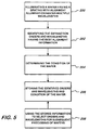
- Fig. 5 is a block diagram illustrating a preferred method or process of practicing the present invention in a learning mode to achieve optimized alignment, irrespective of process variables such as asymmetries or coatings on the wafer grating due to the processing of a wafer during the manufacture of a device.
- block 200 represents the act or step of illuminating a first wafer having a grating thereon with alignment illumination having multiple discrete wavelengths. The discrete wavelengths may be at least four and range between six hundred and thirty and eight hundred and seventy nanometers.
- Block 202 represents the act or step of identifying the diffraction orders and wavelengths having the best alignment information.
- Block 204 represents the act or step of determining the condition of the wafer.
- Block 206 represents the act or step of storing the identified orders, and wavelengths, and condition of the wafer due to the processing variables.
- Block 208 represents the act or step of using the stored information to select identified orders and wavelengths used in subsequent wafer processing on wafers having similar conditions or processing variables.
- the above process steps or method makes it possible for the system to learn or optimize the alignment procedure by looking for specific wavelengths or colors and diffraction orders that provide the most reliable information irrespective of wafer processing variables for obtaining the most accurate alignment. Accordingly, as a result of the apparatus and method of the present invention, alignment of wafers with a mask or reticle is enhanced, improving alignment accuracy and throughput.
- the course alignment 26 is able to detect alignment between the wafer 10 and mask 20 to within a period of the wafer gratings 60 and 68, illustrated in Fig. 2.
- the period of the wafer gratings 60 and 68, illustrated in Fig. 2 should be in the range of one to five microns and is preferably 2.5 microns.
- the fine alignment sensor 30, illustrated in Fig. 1 and Fig. 2 is utilized to achieve an alignment accuracy substantially less than 2.5 microns, and in the order of one nanometer.
- This alignment accuracy is achieved by utilizing a relatively consistent and accurate reference grating 60 that may be made very precisely and that has the same period as a movable grating 68 placed on a wafer to be aligned with a reticle or mask. Any misalignment of the movable wafer grating 68 with respect to the reference grating 60 and a coarse alignment position is detected as a phase shift from a reference signal. This phase shift is utilized by the signal processor 78, illustrated in Fig. 2, to provide misalignment information to a stage controller 128. The stage control 128 causes the wafer stage 12 and the mask stage 22, illustrated in Fig. 1, to move accordingly so as to maintain alignment. The movement of the mask stage 22 is generally referenced to a distance from the fixed reference 62 on which the reference grating 60 is mounted and a coarse alignment position as determined by coarse alignment 26, illustrated in Fig. 1.
- the present invention also has the advantage that it may be easily converted to a latent image metrology (LIM) mode by eliminating the phase measurement aspect. This is made possible by the use of the polarizing output fixture 38 and the central polarizing portion 52 of beamsplitter 50. By rotating the polarizing output fixture 38, the electromagnetic radiation provided to the fixed reference grating 60 can be reduced and/or eliminated. This has the advantage of transforming by command the present invention into a latent image metrology sensor.
- Latent image metrology is a known diagnostic that is desirable in some applications for reducing various critical dimension errors, asymmetries, and aberrations by comparing various order intensities for various latent grating images. Therefore, in some applications, the ability to convert an alignment sensor into a latent image metrology sensor is advantageous.
- the reference phase in the alignment sensor of the present invention comes from the fixed grating 60.
- the objective lens 58 collimates a coherent, monochromatic beam from the reference grating 60. Any of these reference orders is phase locked to a beam of the same wavelength created by the beamsplitter 50. These beams probe the wafer grating 68 and diffract in an identical geometry. As the wafer 10 is scanned in the X direction, phase delay will vary and interference beats will occur. With the use of lossless coatings 54, because of conservation of energy, the beats in orthogonal beams of the same diffracted order must be complimentary and so there is always light or electromagnetic radiation being detected somewhere. As with any interferometer, the phase is arbitrary, but the differences are significant.
- the alignment sensor measures the phase difference with the use of course alignment to remove any ambiguity because of the modulo two-pi error, or shift of one whole wavelength.
- An advantage of the present invention is that the reference grating 60 always has the same predictable diffraction efficiencies. However, the wafer grating 68 has losses and redistribution of efficiencies among the orders. In some applications, it may be useful to balance the reference amplitude for highest fringe contrast. To provide this balancing ability with no phase change, the central part 52 of the beamsplitter 50 may be polarized, while the rest of the beamsplitter 50 is an amplitude splitting coating. Accordingly, by rotating polarization output fixture 38, a balance can be achieved without any unnecessary light loss. This is accomplished by twisting the polarizing output fixture 38 associated with the illuminated source 34. Additionally, the polarizing output fixture 38 can be used to bring the amplitude down to zero, effectively creating the latent image metrology mode previously discussed.
- the present invention has many advantages in improving the alignment between a mask and wafer used in photolithography for the manufacture of semiconductors.
- the use of a fixed reference grating makes it unnecessary to place a high quality grating on each mask or reticle used. A separate and distinct mask alignment mark is allowed.
- the alignment sensor of the present invention can easily be converted for latent image metrology use. Additionally, the use of multiple wavelengths is made possible resulting in a method of optimizing detection and alignment in accordance with various processing variables and asymmetries, thereby enhancing throughput.
Landscapes
- Physics & Mathematics (AREA)
- General Physics & Mathematics (AREA)
- Engineering & Computer Science (AREA)
- Signal Processing (AREA)
- Exposure Of Semiconductors, Excluding Electron Or Ion Beam Exposure (AREA)
- Length Measuring Devices By Optical Means (AREA)
- Exposure And Positioning Against Photoresist Photosensitive Materials (AREA)
Applications Claiming Priority (2)
| Application Number | Priority Date | Filing Date | Title |
|---|---|---|---|
| US371337 | 1995-01-11 | ||
| US09/371,337 US6469793B1 (en) | 1999-08-10 | 1999-08-10 | Multi-channel grating interference alignment sensor |
Publications (3)
| Publication Number | Publication Date |
|---|---|
| EP1076264A2 true EP1076264A2 (de) | 2001-02-14 |
| EP1076264A3 EP1076264A3 (de) | 2005-03-02 |
| EP1076264B1 EP1076264B1 (de) | 2006-08-30 |
Family
ID=23463556
Family Applications (1)
| Application Number | Title | Priority Date | Filing Date |
|---|---|---|---|
| EP00115757A Expired - Lifetime EP1076264B1 (de) | 1999-08-10 | 2000-07-21 | Mehrkanaliges Ausrichtsystem unter Verwendung eines Interferenzgitters |
Country Status (6)
| Country | Link |
|---|---|
| US (1) | US6469793B1 (de) |
| EP (1) | EP1076264B1 (de) |
| JP (1) | JP2001093833A (de) |
| KR (1) | KR100577107B1 (de) |
| CA (1) | CA2314512A1 (de) |
| DE (1) | DE60030374T2 (de) |
Cited By (7)
| Publication number | Priority date | Publication date | Assignee | Title |
|---|---|---|---|---|
| CN103293884A (zh) * | 2012-02-24 | 2013-09-11 | 上海微电子装备有限公司 | 用于光刻设备的离轴对准系统及对准方法 |
| WO2014059811A1 (zh) * | 2012-10-19 | 2014-04-24 | 上海微电子装备有限公司 | 离轴对准系统及对准方法 |
| CN104964649A (zh) * | 2015-07-20 | 2015-10-07 | 哈尔滨工业大学 | 光栅分光式同步移相干涉测量装置及方法 |
| US9201315B2 (en) | 2011-04-22 | 2015-12-01 | Mapper Lithography Ip B.V. | Lithography system for processing a target, such as a wafer, a method for operating a lithography system for processing a target, such as a wafer and a substrate for use in such a lithography system |
| CN105659402A (zh) * | 2013-08-22 | 2016-06-08 | 阿德文泰克全球有限公司 | 使用编码孔径的反射式阴影掩模对准 |
| US9383662B2 (en) | 2011-05-13 | 2016-07-05 | Mapper Lithography Ip B.V. | Lithography system for processing at least a part of a target |
| US9395635B2 (en) | 2011-04-22 | 2016-07-19 | Mapper Lithography Ip B.V. | Position determination in a lithography system using a substrate having a partially reflective position mark |
Families Citing this family (20)
| Publication number | Priority date | Publication date | Assignee | Title |
|---|---|---|---|---|
| US7242464B2 (en) * | 1999-06-24 | 2007-07-10 | Asml Holdings N.V. | Method for characterizing optical systems using holographic reticles |
| US20050010310A1 (en) * | 2003-07-11 | 2005-01-13 | Touzov Igor Victorovich | Method of alignment for precision tools. |
| US6992778B2 (en) * | 2003-08-08 | 2006-01-31 | Mitutoyo Corporation | Method and apparatus for self-calibration of a tunable-source phase shifting interferometer |
| US20080036984A1 (en) * | 2006-08-08 | 2008-02-14 | Asml Netherlands B.V. | Method and apparatus for angular-resolved spectroscopic lithography characterization |
| WO2009028494A1 (ja) * | 2007-08-28 | 2009-03-05 | Nikon Corporation | 位置検出装置、位置検出方法、露光装置、およびデバイス製造方法 |
| DE102008029970A1 (de) * | 2008-06-26 | 2009-12-31 | Carl Zeiss Smt Ag | Projektionsbelichtungsanlage für die Mikrolithographie sowie Verfahren zum Überwachen einer lateralen Abbildungsstabilität |
| NL2007215A (en) | 2010-09-08 | 2012-03-12 | Asml Netherlands Bv | Lithographic apparatus, device manufacturing method, and method of applying a pattern to a substrate. |
| JP5849103B2 (ja) * | 2011-02-01 | 2016-01-27 | ザイゴ コーポレーションZygo Corporation | 干渉ヘテロダイン光学エンコーダシステム |
| CN103135371B (zh) * | 2011-12-02 | 2015-02-11 | 上海微电子装备有限公司 | 基于分束偏折结构的小光斑离轴对准系统 |
| US9030661B1 (en) * | 2013-03-15 | 2015-05-12 | Kla-Tencor Corporation | Alignment measurement system |
| CN103226058B (zh) * | 2013-04-02 | 2015-06-10 | 中国科学院长春光学精密机械与物理研究所 | 一种基于补偿算法的光栅衍射效率的测量方法 |
| CN106796406B (zh) * | 2014-08-25 | 2019-08-30 | Asml控股股份有限公司 | 测量方法、测量设备、光刻设备和器件制造方法 |
| US10883924B2 (en) | 2014-09-08 | 2021-01-05 | The Research Foundation Of State University Of New York | Metallic gratings and measurement methods thereof |
| KR102106937B1 (ko) | 2016-02-19 | 2020-05-07 | 에이에스엠엘 네델란즈 비.브이. | 구조체 측정 방법, 검사 장치, 리소그래피 시스템, 디바이스 제조 방법 및 그 안에 사용되는 파장-선택 필터 |
| WO2017167637A1 (en) | 2016-03-30 | 2017-10-05 | Asml Netherlands B.V. | Substrate edge detection |
| CN107331643B (zh) * | 2016-04-29 | 2021-02-12 | 上海微电子装备(集团)股份有限公司 | 对准装置及其方法 |
| EP3309616A1 (de) * | 2016-10-14 | 2018-04-18 | ASML Netherlands B.V. | Verfahren für die prüfung von einem substrat, metrologievorrichtung und lithografisches system |
| WO2018219639A1 (en) * | 2017-06-02 | 2018-12-06 | Asml Netherlands B.V. | Metrology apparatus |
| KR102689649B1 (ko) | 2019-09-17 | 2024-07-30 | 삼성전자주식회사 | 웨이퍼 검사 장치 |
| CN111751012B (zh) * | 2020-06-03 | 2021-12-14 | 中国科学院西安光学精密机械研究所 | 动态高分辨光学波前相位测量方法 |
Family Cites Families (13)
| Publication number | Priority date | Publication date | Assignee | Title |
|---|---|---|---|---|
| DE3071858D1 (en) * | 1980-07-31 | 1987-01-22 | Ibm | Method and device for optical distance measurement |
| JPS5972728A (ja) | 1982-10-20 | 1984-04-24 | Canon Inc | 自動整合装置 |
| US4631416A (en) | 1983-12-19 | 1986-12-23 | Hewlett-Packard Company | Wafer/mask alignment system using diffraction gratings |
| KR900004269B1 (ko) | 1986-06-11 | 1990-06-18 | 가부시기가이샤 도시바 | 제 1물체와 제 2 물체와의 위치 맞추는 방법 및 장치 |
| JPH0810123B2 (ja) | 1986-09-12 | 1996-01-31 | 株式会社ニコン | 光学装置 |
| EP0323242A3 (de) | 1987-12-28 | 1989-10-18 | Kabushiki Kaisha Toshiba | Verfahren und Vorrichtung zum Ausrichten von zwei Objekten, und Verfahren und Vorrichtung zum Einstellen eines gewünschten Spaltes zwischen zwei Objekten |
| US5171999A (en) * | 1989-02-28 | 1992-12-15 | Nikon Corporation | Adjustable beam and interference fringe position |
| US5151754A (en) | 1989-10-06 | 1992-09-29 | Kabushiki Kaisha Toshiba | Method and an apparatus for measuring a displacement between two objects and a method and an apparatus for measuring a gap distance between two objects |
| JP2893823B2 (ja) * | 1990-03-20 | 1999-05-24 | 株式会社ニコン | 位置合わせ方法及び装置 |
| US5402230A (en) | 1991-12-16 | 1995-03-28 | Tsinghua University | Heterodyne interferometric optical fiber displacement sensor for measuring displacement of an object |
| DE69530757T2 (de) | 1994-01-24 | 2004-03-18 | Asml Holding, N.V. | Gitter-gitter interferometrisches ausrichtsystem |
| US5801390A (en) * | 1996-02-09 | 1998-09-01 | Nikon Corporation | Position-detection method and apparatus with a grating mark |
| US6160622A (en) * | 1997-12-29 | 2000-12-12 | Asm Lithography, B.V. | Alignment device and lithographic apparatus comprising such a device |
-
1999
- 1999-08-10 US US09/371,337 patent/US6469793B1/en not_active Expired - Lifetime
-
2000
- 2000-07-21 EP EP00115757A patent/EP1076264B1/de not_active Expired - Lifetime
- 2000-07-21 DE DE60030374T patent/DE60030374T2/de not_active Expired - Lifetime
- 2000-07-24 CA CA002314512A patent/CA2314512A1/en not_active Abandoned
- 2000-07-29 KR KR1020000043932A patent/KR100577107B1/ko not_active Expired - Fee Related
- 2000-08-08 JP JP2000240007A patent/JP2001093833A/ja active Pending
Cited By (14)
| Publication number | Priority date | Publication date | Assignee | Title |
|---|---|---|---|---|
| US9201315B2 (en) | 2011-04-22 | 2015-12-01 | Mapper Lithography Ip B.V. | Lithography system for processing a target, such as a wafer, a method for operating a lithography system for processing a target, such as a wafer and a substrate for use in such a lithography system |
| US9395635B2 (en) | 2011-04-22 | 2016-07-19 | Mapper Lithography Ip B.V. | Position determination in a lithography system using a substrate having a partially reflective position mark |
| US9395636B2 (en) | 2011-04-22 | 2016-07-19 | Mapper Lithography Ip B.V. | Lithography system for processing a target, such as a wafer, and a method for operating a lithography system for processing a target, such as a wafer |
| US9383662B2 (en) | 2011-05-13 | 2016-07-05 | Mapper Lithography Ip B.V. | Lithography system for processing at least a part of a target |
| CN103293884B (zh) * | 2012-02-24 | 2014-12-17 | 上海微电子装备有限公司 | 用于光刻设备的离轴对准系统及对准方法 |
| CN103293884A (zh) * | 2012-02-24 | 2013-09-11 | 上海微电子装备有限公司 | 用于光刻设备的离轴对准系统及对准方法 |
| KR20150058511A (ko) * | 2012-10-19 | 2015-05-28 | 상하이 마이크로 일렉트로닉스 이큅먼트 컴퍼니 리미티드 | 오프 축 정렬 시스템 및 정렬 방법 |
| CN103777476B (zh) * | 2012-10-19 | 2016-01-27 | 上海微电子装备有限公司 | 一种离轴对准系统及对准方法 |
| CN103777476A (zh) * | 2012-10-19 | 2014-05-07 | 上海微电子装备有限公司 | 一种离轴对准系统及对准方法 |
| WO2014059811A1 (zh) * | 2012-10-19 | 2014-04-24 | 上海微电子装备有限公司 | 离轴对准系统及对准方法 |
| US9448488B2 (en) | 2012-10-19 | 2016-09-20 | Shanghai Micro Electronics Equipment Co., Ltd. | Off-axis alignment system and alignment method |
| CN105659402A (zh) * | 2013-08-22 | 2016-06-08 | 阿德文泰克全球有限公司 | 使用编码孔径的反射式阴影掩模对准 |
| CN105659402B (zh) * | 2013-08-22 | 2019-01-18 | 阿德文泰克全球有限公司 | 使用编码孔径的反射式阴影掩模对准 |
| CN104964649A (zh) * | 2015-07-20 | 2015-10-07 | 哈尔滨工业大学 | 光栅分光式同步移相干涉测量装置及方法 |
Also Published As
| Publication number | Publication date |
|---|---|
| DE60030374T2 (de) | 2006-12-21 |
| US6469793B1 (en) | 2002-10-22 |
| DE60030374D1 (de) | 2006-10-12 |
| KR100577107B1 (ko) | 2006-05-08 |
| CA2314512A1 (en) | 2001-02-10 |
| EP1076264B1 (de) | 2006-08-30 |
| KR20010049931A (ko) | 2001-06-15 |
| JP2001093833A (ja) | 2001-04-06 |
| EP1076264A3 (de) | 2005-03-02 |
Similar Documents
| Publication | Publication Date | Title |
|---|---|---|
| EP1076264B1 (de) | Mehrkanaliges Ausrichtsystem unter Verwendung eines Interferenzgitters | |
| KR100700444B1 (ko) | 자체 기준 마크의 독립 정렬 센서 | |
| US5333050A (en) | Measuring method and apparatus for meausring the positional relationship of first and second gratings | |
| US4728193A (en) | Precision automatic mask-wafer alignment system | |
| US5202748A (en) | In situ process control system for steppers | |
| US5751426A (en) | Positional deviation measuring device and method for measuring the positional deviation between a plurality of diffraction gratings formed on the same object | |
| KR102388682B1 (ko) | 계측 방법 및 디바이스 | |
| WO2006107929A1 (en) | Determining positional error of an optical component using structured light patterns | |
| US5831739A (en) | Alignment method | |
| JP7435703B2 (ja) | 面位置検出装置、露光装置、デバイス製造方法、および基板処理システム | |
| US5585923A (en) | Method and apparatus for measuring positional deviation while correcting an error on the basis of the error detection by an error detecting means | |
| US5654540A (en) | High resolution remote position detection using segmented gratings | |
| JPH08219718A (ja) | 面位置検出装置 | |
| JP2009170666A (ja) | 計測装置及び光強度分布計測方法、露光装置 | |
| EP4567371A1 (de) | Metrologievorrichtung und zugehörige verfahren | |
| JPH09293663A (ja) | 位置検出装置及び該装置を備えた露光装置 | |
| JP3111556B2 (ja) | 微細パターンの形成装置 | |
| JPH0587530A (ja) | 干渉計測装置 | |
| JPH08162393A (ja) | 位置合わせ装置 | |
| US8422027B2 (en) | Imaging optical system for producing control information regarding lateral movement of an image plane or an object plane | |
| JP2667589B2 (ja) | 光露光装置のアラインメント装置 | |
| JP2683409B2 (ja) | 位置合わせ装置 | |
| JPH0540024A (ja) | 形状測定システム | |
| JPH07119575B2 (ja) | 露光装置 | |
| JPH08124835A (ja) | アライメント装置 |
Legal Events
| Date | Code | Title | Description |
|---|---|---|---|
| PUAI | Public reference made under article 153(3) epc to a published international application that has entered the european phase |
Free format text: ORIGINAL CODE: 0009012 |
|
| AK | Designated contracting states |
Kind code of ref document: A2 Designated state(s): AT BE CH CY DE DK ES FI FR GB GR IE IT LI LU MC NL PT SE |
|
| AX | Request for extension of the european patent |
Free format text: AL;LT;LV;MK;RO;SI |
|
| PUAL | Search report despatched |
Free format text: ORIGINAL CODE: 0009013 |
|
| AK | Designated contracting states |
Kind code of ref document: A3 Designated state(s): AT BE CH CY DE DK ES FI FR GB GR IE IT LI LU MC NL PT SE |
|
| AX | Request for extension of the european patent |
Extension state: AL LT LV MK RO SI |
|
| 17P | Request for examination filed |
Effective date: 20050217 |
|
| 17Q | First examination report despatched |
Effective date: 20050608 |
|
| AKX | Designation fees paid |
Designated state(s): DE FR GB IT NL |
|
| GRAP | Despatch of communication of intention to grant a patent |
Free format text: ORIGINAL CODE: EPIDOSNIGR1 |
|
| RTI1 | Title (correction) |
Free format text: MULTI-CHANNEL GRATING INTERFERENCE ALIGNMENT SYSTEM |
|
| RAP1 | Party data changed (applicant data changed or rights of an application transferred) |
Owner name: ASML HOLDING N.V. |
|
| GRAS | Grant fee paid |
Free format text: ORIGINAL CODE: EPIDOSNIGR3 |
|
| GRAA | (expected) grant |
Free format text: ORIGINAL CODE: 0009210 |
|
| AK | Designated contracting states |
Kind code of ref document: B1 Designated state(s): DE FR GB IT NL |
|
| PG25 | Lapsed in a contracting state [announced via postgrant information from national office to epo] |
Ref country code: IT Free format text: LAPSE BECAUSE OF FAILURE TO SUBMIT A TRANSLATION OF THE DESCRIPTION OR TO PAY THE FEE WITHIN THE PRE;WARNING: LAPSES OF ITALIAN PATENTS WITH EFFECTIVE DATE BEFORE 2007 MAY HAVE OCCURRED AT ANY TIME BEFORE 2007. THE CORRECT EFFECTIVE DATE MAY BE DIFFERENT FROM THE ONE RECORDED.SCRIBED TIME-LIMIT Effective date: 20060830 |
|
| REG | Reference to a national code |
Ref country code: GB Ref legal event code: FG4D |
|
| REF | Corresponds to: |
Ref document number: 60030374 Country of ref document: DE Date of ref document: 20061012 Kind code of ref document: P |
|
| ET | Fr: translation filed | ||
| PLBE | No opposition filed within time limit |
Free format text: ORIGINAL CODE: 0009261 |
|
| STAA | Information on the status of an ep patent application or granted ep patent |
Free format text: STATUS: NO OPPOSITION FILED WITHIN TIME LIMIT |
|
| 26N | No opposition filed |
Effective date: 20070531 |
|
| PGFP | Annual fee paid to national office [announced via postgrant information from national office to epo] |
Ref country code: IT Payment date: 20080724 Year of fee payment: 9 Ref country code: NL Payment date: 20080716 Year of fee payment: 9 |
|
| PGFP | Annual fee paid to national office [announced via postgrant information from national office to epo] |
Ref country code: GB Payment date: 20080722 Year of fee payment: 9 |
|
| GBPC | Gb: european patent ceased through non-payment of renewal fee |
Effective date: 20090721 |
|
| NLV4 | Nl: lapsed or anulled due to non-payment of the annual fee |
Effective date: 20100201 |
|
| PG25 | Lapsed in a contracting state [announced via postgrant information from national office to epo] |
Ref country code: GB Free format text: LAPSE BECAUSE OF NON-PAYMENT OF DUE FEES Effective date: 20090721 |
|
| PG25 | Lapsed in a contracting state [announced via postgrant information from national office to epo] |
Ref country code: IT Free format text: LAPSE BECAUSE OF NON-PAYMENT OF DUE FEES Effective date: 20090721 |
|
| PG25 | Lapsed in a contracting state [announced via postgrant information from national office to epo] |
Ref country code: NL Free format text: LAPSE BECAUSE OF NON-PAYMENT OF DUE FEES Effective date: 20100201 |
|
| REG | Reference to a national code |
Ref country code: FR Ref legal event code: PLFP Year of fee payment: 17 |
|
| PGFP | Annual fee paid to national office [announced via postgrant information from national office to epo] |
Ref country code: DE Payment date: 20160722 Year of fee payment: 17 |
|
| PGFP | Annual fee paid to national office [announced via postgrant information from national office to epo] |
Ref country code: FR Payment date: 20160721 Year of fee payment: 17 |
|
| REG | Reference to a national code |
Ref country code: DE Ref legal event code: R119 Ref document number: 60030374 Country of ref document: DE |
|
| REG | Reference to a national code |
Ref country code: FR Ref legal event code: ST Effective date: 20180330 |
|
| PG25 | Lapsed in a contracting state [announced via postgrant information from national office to epo] |
Ref country code: DE Free format text: LAPSE BECAUSE OF NON-PAYMENT OF DUE FEES Effective date: 20180201 |
|
| PG25 | Lapsed in a contracting state [announced via postgrant information from national office to epo] |
Ref country code: FR Free format text: LAPSE BECAUSE OF NON-PAYMENT OF DUE FEES Effective date: 20170731 |