EP1089595A2 - Dispositif d'affichage électroluminescent organique - Google Patents
Dispositif d'affichage électroluminescent organique Download PDFInfo
- Publication number
- EP1089595A2 EP1089595A2 EP00121499A EP00121499A EP1089595A2 EP 1089595 A2 EP1089595 A2 EP 1089595A2 EP 00121499 A EP00121499 A EP 00121499A EP 00121499 A EP00121499 A EP 00121499A EP 1089595 A2 EP1089595 A2 EP 1089595A2
- Authority
- EP
- European Patent Office
- Prior art keywords
- organic
- display device
- cover plate
- bed
- semiconductor substrate
- Prior art date
- Legal status (The legal status is an assumption and is not a legal conclusion. Google has not performed a legal analysis and makes no representation as to the accuracy of the status listed.)
- Granted
Links
Images


Classifications
-
- H—ELECTRICITY
- H05—ELECTRIC TECHNIQUES NOT OTHERWISE PROVIDED FOR
- H05B—ELECTRIC HEATING; ELECTRIC LIGHT SOURCES NOT OTHERWISE PROVIDED FOR; CIRCUIT ARRANGEMENTS FOR ELECTRIC LIGHT SOURCES, IN GENERAL
- H05B33/00—Electroluminescent light sources
- H05B33/02—Details
- H05B33/04—Sealing arrangements, e.g. against humidity
-
- H—ELECTRICITY
- H05—ELECTRIC TECHNIQUES NOT OTHERWISE PROVIDED FOR
- H05B—ELECTRIC HEATING; ELECTRIC LIGHT SOURCES NOT OTHERWISE PROVIDED FOR; CIRCUIT ARRANGEMENTS FOR ELECTRIC LIGHT SOURCES, IN GENERAL
- H05B33/00—Electroluminescent light sources
-
- H—ELECTRICITY
- H10—SEMICONDUCTOR DEVICES; ELECTRIC SOLID-STATE DEVICES NOT OTHERWISE PROVIDED FOR
- H10K—ORGANIC ELECTRIC SOLID-STATE DEVICES
- H10K50/00—Organic light-emitting devices
- H10K50/80—Constructional details
- H10K50/84—Passivation; Containers; Encapsulations
-
- H—ELECTRICITY
- H10—SEMICONDUCTOR DEVICES; ELECTRIC SOLID-STATE DEVICES NOT OTHERWISE PROVIDED FOR
- H10K—ORGANIC ELECTRIC SOLID-STATE DEVICES
- H10K50/00—Organic light-emitting devices
- H10K50/80—Constructional details
- H10K50/84—Passivation; Containers; Encapsulations
- H10K50/841—Self-supporting sealing arrangements
-
- H—ELECTRICITY
- H10—SEMICONDUCTOR DEVICES; ELECTRIC SOLID-STATE DEVICES NOT OTHERWISE PROVIDED FOR
- H10K—ORGANIC ELECTRIC SOLID-STATE DEVICES
- H10K50/00—Organic light-emitting devices
- H10K50/80—Constructional details
- H10K50/84—Passivation; Containers; Encapsulations
- H10K50/846—Passivation; Containers; Encapsulations comprising getter material or desiccants
-
- H—ELECTRICITY
- H10—SEMICONDUCTOR DEVICES; ELECTRIC SOLID-STATE DEVICES NOT OTHERWISE PROVIDED FOR
- H10K—ORGANIC ELECTRIC SOLID-STATE DEVICES
- H10K50/00—Organic light-emitting devices
- H10K50/80—Constructional details
- H10K50/85—Arrangements for extracting light from the devices
- H10K50/858—Arrangements for extracting light from the devices comprising refractive means, e.g. lenses
-
- H—ELECTRICITY
- H10—SEMICONDUCTOR DEVICES; ELECTRIC SOLID-STATE DEVICES NOT OTHERWISE PROVIDED FOR
- H10K—ORGANIC ELECTRIC SOLID-STATE DEVICES
- H10K59/00—Integrated devices, or assemblies of multiple devices, comprising at least one organic light-emitting element covered by group H10K50/00
- H10K59/10—OLED displays
- H10K59/12—Active-matrix OLED [AMOLED] displays
- H10K59/131—Interconnections, e.g. wiring lines or terminals
-
- H—ELECTRICITY
- H10—SEMICONDUCTOR DEVICES; ELECTRIC SOLID-STATE DEVICES NOT OTHERWISE PROVIDED FOR
- H10K—ORGANIC ELECTRIC SOLID-STATE DEVICES
- H10K59/00—Integrated devices, or assemblies of multiple devices, comprising at least one organic light-emitting element covered by group H10K50/00
- H10K59/80—Constructional details
- H10K59/87—Passivation; Containers; Encapsulations
- H10K59/871—Self-supporting sealing arrangements
-
- H—ELECTRICITY
- H10—SEMICONDUCTOR DEVICES; ELECTRIC SOLID-STATE DEVICES NOT OTHERWISE PROVIDED FOR
- H10K—ORGANIC ELECTRIC SOLID-STATE DEVICES
- H10K59/00—Integrated devices, or assemblies of multiple devices, comprising at least one organic light-emitting element covered by group H10K50/00
- H10K59/80—Constructional details
- H10K59/875—Arrangements for extracting light from the devices
- H10K59/879—Arrangements for extracting light from the devices comprising refractive means, e.g. lenses
-
- H—ELECTRICITY
- H10—SEMICONDUCTOR DEVICES; ELECTRIC SOLID-STATE DEVICES NOT OTHERWISE PROVIDED FOR
- H10K—ORGANIC ELECTRIC SOLID-STATE DEVICES
- H10K59/00—Integrated devices, or assemblies of multiple devices, comprising at least one organic light-emitting element covered by group H10K50/00
- H10K59/80—Constructional details
- H10K59/8791—Arrangements for improving contrast, e.g. preventing reflection of ambient light
-
- H—ELECTRICITY
- H10—SEMICONDUCTOR DEVICES; ELECTRIC SOLID-STATE DEVICES NOT OTHERWISE PROVIDED FOR
- H10K—ORGANIC ELECTRIC SOLID-STATE DEVICES
- H10K2102/00—Constructional details relating to the organic devices covered by this subclass
- H10K2102/301—Details of OLEDs
- H10K2102/302—Details of OLEDs of OLED structures
- H10K2102/3023—Direction of light emission
- H10K2102/3026—Top emission
-
- H—ELECTRICITY
- H10—SEMICONDUCTOR DEVICES; ELECTRIC SOLID-STATE DEVICES NOT OTHERWISE PROVIDED FOR
- H10K—ORGANIC ELECTRIC SOLID-STATE DEVICES
- H10K50/00—Organic light-emitting devices
- H10K50/80—Constructional details
- H10K50/86—Arrangements for improving contrast, e.g. preventing reflection of ambient light
-
- H—ELECTRICITY
- H10—SEMICONDUCTOR DEVICES; ELECTRIC SOLID-STATE DEVICES NOT OTHERWISE PROVIDED FOR
- H10K—ORGANIC ELECTRIC SOLID-STATE DEVICES
- H10K59/00—Integrated devices, or assemblies of multiple devices, comprising at least one organic light-emitting element covered by group H10K50/00
- H10K59/80—Constructional details
- H10K59/87—Passivation; Containers; Encapsulations
- H10K59/874—Passivation; Containers; Encapsulations including getter material or desiccant
Definitions
- the present invention relates to a semiconductor device having a circuit based on insulated-gate field effect transistors in which a single-crystal semiconductor is used for an active layer, and a method of fabricating the semiconductor device. More particularly, the present invention is well suited for applications to an electrooptic device which is typified by an organic electroluminescent display device wherein the same substrate is overlaid with a pixel unit and driver circuits disposed around the pixel unit, and to an electronic apparatus in which the electrooptic device is installed.
- the expression "semiconductor device” is intended to signify general devices which function by utilizing semiconductor properties, and it shall cover within its category the electrooptic device and the electronic equipment including this electrooptic device.
- TFTs thin-film transistors
- LSIs large-scale integrated circuits
- the FETs of high performance which are capable of low-voltage drive at high speed can be integrated and formed at a high density on the substrate.
- the display device is restricted to one of reflection type or spontaneous luminescence type because the substrate is opaque to visible light, or that the single-crystal semiconductor substrate is restricted to sizes available on the market.
- the active matrix type display device is so constructed that transistors (such as TFTs or FETs) in the number of several tens to several millions are arranged in a pixel unit for displaying an image, and that pixel electrodes are respectively connected to the transistors.
- the image is displayed in such a way that voltages to be applied to respective pixels are controlled by the switching functions of the corresponding transistors, whereby some of EL elements are caused to luminesce.
- the switching transistors disposed in the respective pixels are turned ON, currents are caused to flow through current controlling transistors by signals generated in accordance with image data, whereby the EL elements luminesce spontaneously.
- an organic EL layer which serves as the basic portion of the organic EL display device is very liable to oxidize, and it easily deteriorates in the presence of a slight amount of oxygen. Besides, it has a low becomes a cause for resistance to heat, and this also is a factor promoting oxidation.
- the liability to oxidize is the cause of a short lifetime of the organic EL element, and has formed a serious obstacle in putting this element into practical use.
- the object of the present invention is to overcome the problem as stated above, and to provide an organic EL display device of high reliability.
- Another object of the present invention is to provide an electron device whose display unit is highly reliable, by adopting such an organic EL display device for the display unit.
- the construction of the present invention for accomplishing the objects consists in an organic EL display device of active matrix type wherein insulated-gate field effect transistors formed on a single-crystal semiconductor substrate are overlaid with an organic EL layer; characterized in that the single-crystal semiconductor substrate is held in a vacant space which is defined by a bed plate and a cover plate formed of an insulating material and a packing material for bonding the bed and cover plates; and that the vacant space is filled with an inert gas and a drying agent.
- the construction of the present invention consists in an organic EL display device of active matrix type having a pixel unit wherein insulated-gate field effect transistors formed on a single-crystal semiconductor substrate are overlaid with an organic EL layer; characterized in that the single-crystal semiconductor substrate is held in a vacant space which is defined by a bed plate and a cover plate formed of an insulating material, and a packing material for bonding the bed and cover plates; that the cover plate is formed of a transparent member in its area which lies over the pixel unit; and that the vacant space is filled with an inert gas and a drying agent.
- a single-crystal silicon substrate can be favorably employed as the single-crystal semiconductor substrate.
- the vacant space should preferably be filled with an inert gas selected from the group consisting of helium, argon, krypton, xenon and nitrogen, and a drying agent selected from the group consisting of barium oxide and silica gel.
- the organic EL display device according to the present invention has such a structure that a pixel unit and driver circuits around the pixel unit are disposed using field effect transistors (FETs) of insulated gate type which are formed on a single-crystal semiconductor substrate (for example, single-crystal silicon substrate).
- FETs field effect transistors
- a substrate 101 is made of single-crystal silicon having a comparatively high resistance(for example, one of n-type at about 10 [ ⁇ cm]), and a p-well 102 and n-wells 103 ⁇ 105 are formed in self-alignment therein. Adjacent FETs are isolated by a field oxide film 106. In forming the field oxide film 106, channel stoppers may be formed by introducing boron (B) into the selected parts of the substrate 101 in accordance with ion implantation.
- B boron
- Gate insulating films 110, 116, 122 and 128 are formed by thermal oxidation.
- Gates 111, 117, 123 and 129 consist of polycrystalline silicon layers 111a, 117a, 123a and 129a formed from a polycrystalline silicon film deposited to a thickness of 100 ⁇ 300 [nm] by CVD, and suicide layers 111b, 117b, 123b and 129b formed thereon to a thickness of 50 ⁇ 300 [nm], respectively.
- the polycrystalline silicon layers may be doped with phosphorus (P) at a concentration of 10 21 [/cm 3 ] or so beforehand in order to lower the resistance thereof, or an n-type impurity at a high concentration may be diffused after the polycrystalline silicon film has been formed.
- P phosphorus
- the material of the suicide layers is any of molybdenum silicide (MoSi x ), tungsten suicide (WSi x ), tantalum suicide (TaSi x ), titanium silicide (TiSi x ), etc., and the silicide layers may well be formed in accordance with a known method.
- MoSi x molybdenum silicide
- WSi x tungsten suicide
- TaSi x tantalum suicide
- TiSi x titanium silicide
- the silicide layers may well be formed in accordance with a known method.
- the lightly-doped drain (LDD) regions 107 of a p-channel FET 201 are doped with boron (B) at a dose of 1 ⁇ 10 13 ⁇ 1 ⁇ 10 14 [/cm 2 ] as an impurity element which bestows the conductivity type of p-type.
- the LDD regions 113 of an n-channel FET 202, and those 119 and 125 of a switching FET 203 and a current controlling FET 204 made up of n-channel FETs are doped with phosphorus (P) or arsenic (As) as the impurity element which bestows n-type conductivity, at a dose similar to that of p-type.
- These LDD regions are respectively formed in self-alignment in accordance with ion implantation or ion doping by employing the corresponding gates as masks.
- Side wall spacers 112, 118, 124 and 130 are formed in such away that, after the formation of the LDD regions, an insulating film such as silicon oxide film or silicon nitride film is formed on the whole surface of the resulting substrate by CVD, and that the insulating film is uniformly etched over the whole area thereof by anisotropic dry etching, so as to be left behind on the side walls of the corresponding gates.
- the source regions and drain regions of the respective FETs are formed by employing the corresponding side wall spacers as masks.
- the source region 108 and drain region 109 of the p-channel FET 201 is formed by ion-implanting boron (B) at a dose of 5 ⁇ 10 14 ⁇ 1 ⁇ 10 16 [/cm 2 ].
- the n-channel FET 202, and the switching FET 203 and current controlling FET 204 made up of these n-channel FETs are respectively formed with the source regions 114, 120 and 126 and drain regions 115, 121 and 127 by ion-implanting arsenic (As) at a dose of 5 ⁇ 10 14 ⁇ 1 ⁇ 10 16 [/cm 2 ].
- a first interlayer insulating film 131 is formed to a thickness of 100 ⁇ 2000 nm out of a silicon oxide film, an oxidized silicon nitride film or the like which should preferably be prepared by plasma CVD or low-pressure CVD. Further, the first interlayer insulating film 131 is overlaid with a second interlayer insulating film 132 which is made of phosphosilicate glass (PSG), borosilicate glass (BSG) or phosphoborosilicate glass (PBSG). The second Interlayer insulating film 132 is prepared by spin coating or normal-pressure CVD.
- the prepared film is caused to reflow by a treatment of thermal activation at 700 ⁇ 900 [°C], which is carried out after the preparation and which serves also as a heat treatment, whereby the surface of the second interlayer insulating film 132 is flattened.
- Source wiring lines 133, 135, 137 and 139 and drain wiring lines 134, 136, 138 and 140 are respectively formed after contact holes reaching the source regions and drain regions of the corresponding FETs are formed in the first interlayer insulating film 131 and the flattened film 132.
- Aluminum (Al) which is usually and often used as a low-resistance material, may be employed for the wiring lines.
- a multilayer structure consisting of an Al layer and a titanium (Ti) layer may be employed for each of the wiring lines.
- a passivation film 141 is formed of a silicon nitride film, a silicon oxide film or a nitrified silicon oxide film by plasma CVD. Further, a third interlayer insulating film 142 is formed of an organic resin material to a thickness of 1 [ ⁇ m] ⁇ 2 [ ⁇ m]. Any of the following: a polyimide resin, a polyamide resin, an acrylic resin, benzo-cyclo-butene (BCB), etc. can be used as the organic resin material. The merits of the use of the organic resin material are that a method of forming the film is simple, that parasitic capacitance can be lowered owing to a low relative dielectric constant, that the material is suited to be flattened, and so forth. Of course, any organic resin film other than mentioned above may be employed.
- the polyimide resin of the type which is applied on the resulting substrate and then is treated by thermal polymerization is employed, and it is baked at 300 [°C] in a clean oven.
- a pixel electrode 143 is connected to the drain wiring line of the current controlling FET 204.
- the pixel electrode 143 is formed of a low-resistivity material typified by Al.
- An Al film can be readily formed by a known method of forming the film, for example, vacuum deposition or sputtering.
- the surface of the pixel electrode 143 may be roughened into a diffusing reflective surface.
- cathode layers 144 containing a metal of low work function are formed on all the pixel electrodes. Since the cathode layer 144 is as thin as a few nm or so, whether a true layer is formed or it exists sporadically in the shape of islands is unclear, and hence, its contour is indicated by a broken line.
- a material which is usable as the cathode layer 144 containing the metal of low work function is lithium fluoride (LiF), lithium oxide (Li 2 O), barium fluoride (BaF 2 ), barium oxide (BaO), calcium fluoride (CaF 2 ), calcium oxide (CaO), strontium oxide (SrO) or cesium oxide (Cs 2 O). Since the material is insulating, the short-circuiting between the pixel electrodes is not incurred even when the cathode layer 144 is a connecting layer.
- a cathode layer made of a known material having conductivity, such as MgAg electrode can be used as the cathode layer. It is necessary, however, to form cathodes themselves selectively or to perform patterning, so as to prevent the pixel electrodes from short-circuiting.
- An organic EL (e lectro l uminescent) layer 145 is formed on the cathode layer 144 containing the metal of low work function.
- a known material or structure can be employed for the organic EL layer 145, a material capable of white luminescence is used in the present invention.
- the organic EL layer 145 may be formed of nothing but a luminescent layer which offers a site for recombination. If necessary, it is also allowed to stack on this an electron injection layer, an electron transport layer, a hole transport layer, an electron blocking layer, a hole blocking layer or a hole injection layer.
- all the layers where carriers are injected, transported or recombined shall be comprehensively called the "organic EL layer”.
- the organic EL material used for the organic EL layer 145 is a high-molecular one based on a polymer.
- the organic EL layer 145 is formed in such a way that PVK (polyvinyl carbazole), Bu-PBD (2-(4'-tert-butylphenyl)-5-(4''-biphenyl)-1, 3, 4-oxadiazole), coumarin 6, DCM 1 (4-dicyanomethylene-2-methyl-6-p-dimethylaminostyryl -4H-pyran), TPB (tetraphenylbutadiene) and Nile red are dissolved in 1, 2-dichloromethane or chloroform, and that a solution thus obtained is applied by spin coating.
- the substrate structure coated with the solution is rotated at a rotational frequency of about 500 ⁇ 1000 [rpm] for 20 ⁇ 60 [seconds], whereby a uniform coating film is formed.
- the coating film is formed after the organic EL material is refined (typically, by dialyzing) at least 3 times, preferably 5 times or more, thereby to lower the sodium content of this material to 0.1 [ppm] or less (preferably, 0.01 [ppm] or less).
- the sodium content of the organic EL layer 349 becomes 0.1 [ppm] or less (preferably, 0.01 [ppm] or less)
- the volume resistance thereof becomes 1 ⁇ 10 11 ⁇ 1 ⁇ 10 12 [ ⁇ cm] (preferably, 1 ⁇ 10 12 ⁇ 1 ⁇ 10 13 [ ⁇ cm]).
- the organic EL layer 145 formed in this way is overlaid with a transparent conductive film as an anode layer 146.
- a transparent conductive film is a compound (called "ITO") produced from indium oxide and tin oxide, a compound produced from indium oxide and zinc oxide, tin oxide (SnO 2 ), zinc oxide (ZnO), or the like.
- the anode layer 146 is overlaid with an insulating film as a passivation film 147.
- the passivation film 147 should preferably be a silicon nitride film or a nitrified silicon oxide film (expressed by "SiO x N y ").
- the substrate structure completed up to this point in this specification shall be called “active matrix substrate”. That is, the “active matrix substrate” is the substrate which is formed with the FETs, the pixel electrodes electrically connected to the FETs, and organic EL elements including pixel electrodes as the cathodes (capacitors consisting of the cathode layers, the organic EL layer and the anodes).
- Fig. 2(A) is a top plan view of the pixel unit of the active matrix substrate
- Fig. 2(B) is a connection diagram of the circuit arrangement of the pixel unit.
- the pixel unit image display unit
- the pixel unit is so constructed that a plurality of pixels are arrayed in the shape of a matrix.
- a sectional view taken along A - A' in Fig. 2(A) corresponds to the sectional view of the pixel unit in Fig. 1.
- common reference numerals are indicated in Fig. 1 and Fig. 2(A), both of which may be referred to on occasion.
- two pixels are illustrated in the top plan view of Fig. 2(A), and they have the same structure.
- two FETs per pixel are disposed for the organic EL element 205. Both the FETs are of n-channel type, and they function as the switching FET 203 and the current controlling FET 204.
- driver circuits each of which is based on a CMOS circuit configured with a p-channel FET 201 and a n-channel FET 202, and pixel units each of which includes switching FET 203 and current controlling FET 204 formed of n-channel FETs.
- the driver circuits based on the CMOS circuits can form, for example, a shift register circuit, a buffer circuit, a sampling circuit, a D/A converter, and a latch circuit.
- Fig. 3 is a top plan view showing an active matrix substrate.
- the active matrix substrate includes a substrate 1000, a pixel unit 1001, data line side driver circuits 1003, and scanning line side driver circuits 1002.
- Input terminals for the respective driver circuits are pads 1006 for wire bonding which are disposed near the edges of the substrate 1000, and they are connected to the driver circuits via leads 1004 ⁇ 1005.
- the pixel unit having a size of from 0.5-inch class to 2.5-inch class is well suited for fabrication.
- the active matrix substrate formed with the organic EL layer is sealed in a package in order to be cut off from external shocks, and ambient conditions such as dust and humidity.
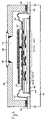
- the shape and scheme of the package are exemplified in Fig. 4.
- a bed plate 401 is formed of an insulating material such as ceramics, and the active matrix substrate 413 formed with the organic EL layer is fixed thereon by a low-melting glass or metallized layer 402.
- the active matrix substrate 413 is connected with an external circuit by a lead frame 404, which is connected with the active matrix substrate 413 by wire pieces 412 of gold (Au) through pads 410 for wire bonding.
- the active matrix substrate 413 is sealed with a cover ceramic plate 405.
- the ceramic cover plate 405 is bonded with the bed plate 401 by a binder layer 404.
- Pyroceram cement, bismuth oxide-based glass, lead oxide-based glass, or the like is used for the binder layer 404.
- a window member 406 made of a transparent quartz plate, a transparent glass plate or the like is mounted and fixed with adhesives 407 in an area where the cover plate 405 formed of the ceramics or the like insulating material similarly to the bed plate 401 lies over the pixel unit of the active matrix substrate 413. In this way, the active matrix substrate 413 formed with the organic EL layer is enclosed, and a vacant space 414 is formed.
- the vacant space 414 should desirably be filled with an inert gas (such as argon, helium, krypton, xenon or nitrogen) or have a drying agent (such as barium oxide) put therein. In this way it is possible to suppress the deterioration of the EL element attributed to moisture etc.
- an inert gas such as argon, helium, krypton, xenon or nitrogen
- a drying agent such as barium oxide
- a color display can also be constructed by disposing color filters or black matrix layers (light intercepting layers) on the organic EL layer in correspondence with the individual pixels formed from the organic EL layer of the active matrix substrate.
- color filters may well be disposed at the window 406 shown in Fig. 4.
- the lead frame 403 is connected to the terminals of the external equipment, whereby an image signal etc. can be inputted to display an image on the pixel unit.
- an article which is brought into a state where it is capable of displaying an image, by attaching a lead frame to an external circuit is defined as an "organic EL display device”.
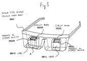
- FIG. 5 shows a schematic view of the goggle type display device in this example.
- the goggle type display device main body 3600 is furnished with two, right and left display units, which are constructed of organic EL display devices 3602R, 3602L, circuit boards 3603R, 3603L and lenses 3601R, 3601L.
- Fig. 6(A) shows a sectional view of part A indicated in Fig. 5, while Fig. 6(B) shows an enlarged view of part B indicated in Fig. 6(A).
- the organic EL display device 3602R mounted on the lens 3601R is connected to the circuit board 3603R equipped with a signal control circuit etc., through a lead frame 3606R.
- Light luminescing from the organic EL display device 3602R arrives at the eyeball 3604R of a user via an optical path indicated by arrows in Fig. 6(A), whereby the user can recognize an image.
- the organic EL display device has a wide view angle owing to its spontaneous luminescence. When applied to the goggle type display device, the organic EL display is not spoilt even if the relative positions of this display device and an observer's eye have deviated.
Landscapes
- Engineering & Computer Science (AREA)
- Microelectronics & Electronic Packaging (AREA)
- Physics & Mathematics (AREA)
- Optics & Photonics (AREA)
- Electroluminescent Light Sources (AREA)
- Devices For Indicating Variable Information By Combining Individual Elements (AREA)
Priority Applications (1)
| Application Number | Priority Date | Filing Date | Title |
|---|---|---|---|
| EP06025256A EP1777994B1 (fr) | 1999-09-30 | 2000-09-29 | Dispositif d'affichage électroluminescent organique |
Applications Claiming Priority (2)
| Application Number | Priority Date | Filing Date | Title |
|---|---|---|---|
| JP27987099 | 1999-09-30 | ||
| JP27987099 | 1999-09-30 |
Related Child Applications (1)
| Application Number | Title | Priority Date | Filing Date |
|---|---|---|---|
| EP06025256A Division EP1777994B1 (fr) | 1999-09-30 | 2000-09-29 | Dispositif d'affichage électroluminescent organique |
Publications (3)
| Publication Number | Publication Date |
|---|---|
| EP1089595A2 true EP1089595A2 (fr) | 2001-04-04 |
| EP1089595A3 EP1089595A3 (fr) | 2002-01-23 |
| EP1089595B1 EP1089595B1 (fr) | 2007-01-24 |
Family
ID=17617104
Family Applications (2)
| Application Number | Title | Priority Date | Filing Date |
|---|---|---|---|
| EP00121499A Expired - Lifetime EP1089595B1 (fr) | 1999-09-30 | 2000-09-29 | Dispositif d'affichage électroluminescent organique |
| EP06025256A Expired - Lifetime EP1777994B1 (fr) | 1999-09-30 | 2000-09-29 | Dispositif d'affichage électroluminescent organique |
Family Applications After (1)
| Application Number | Title | Priority Date | Filing Date |
|---|---|---|---|
| EP06025256A Expired - Lifetime EP1777994B1 (fr) | 1999-09-30 | 2000-09-29 | Dispositif d'affichage électroluminescent organique |
Country Status (5)
| Country | Link |
|---|---|
| US (5) | US6876145B1 (fr) |
| EP (2) | EP1089595B1 (fr) |
| KR (1) | KR100747418B1 (fr) |
| CN (2) | CN1877851A (fr) |
| DE (2) | DE60033103T2 (fr) |
Cited By (2)
| Publication number | Priority date | Publication date | Assignee | Title |
|---|---|---|---|---|
| EP1521505A1 (fr) * | 2003-10-02 | 2005-04-06 | Hewlett-Packard Development Company, L.P. | Dispositif électroluminescent |
| EP1450334A4 (fr) * | 2002-01-16 | 2007-11-21 | Seiko Epson Corp | Dispositif d'affichage |
Families Citing this family (49)
| Publication number | Priority date | Publication date | Assignee | Title |
|---|---|---|---|---|
| US6617644B1 (en) * | 1998-11-09 | 2003-09-09 | Semiconductor Energy Laboratory Co., Ltd. | Semiconductor device and method of manufacturing the same |
| US6909114B1 (en) | 1998-11-17 | 2005-06-21 | Semiconductor Energy Laboratory Co., Ltd. | Semiconductor device having LDD regions |
| US6277679B1 (en) | 1998-11-25 | 2001-08-21 | Semiconductor Energy Laboratory Co., Ltd. | Method of manufacturing thin film transistor |
| US6677613B1 (en) * | 1999-03-03 | 2004-01-13 | Semiconductor Energy Laboratory Co., Ltd. | Semiconductor device and method of fabricating the same |
| US6876145B1 (en) * | 1999-09-30 | 2005-04-05 | Semiconductor Energy Laboratory Co., Ltd. | Organic electroluminescent display device |
| US6580094B1 (en) | 1999-10-29 | 2003-06-17 | Semiconductor Energy Laboratory Co., Ltd. | Electro luminescence display device |
| US6724150B2 (en) * | 2001-02-01 | 2004-04-20 | Semiconductor Energy Laboratory Co., Ltd. | Display device and manufacturing method thereof |
| US6975304B1 (en) * | 2001-06-11 | 2005-12-13 | Handspring, Inc. | Interface for processing of an alternate symbol in a computer device |
| GB2381658B (en) * | 2001-07-25 | 2004-03-03 | Lg Philips Lcd Co Ltd | Active matrix organic electroluminescent device simplifying a fabricating process and a fabricating method thereof |
| JP2003114646A (ja) * | 2001-08-03 | 2003-04-18 | Semiconductor Energy Lab Co Ltd | 表示装置及びその駆動方法。 |
| JP4149168B2 (ja) * | 2001-11-09 | 2008-09-10 | 株式会社半導体エネルギー研究所 | 発光装置 |
| US7042024B2 (en) * | 2001-11-09 | 2006-05-09 | Semiconductor Energy Laboratory Co., Ltd. | Light emitting apparatus and method for manufacturing the same |
| AU2003288999A1 (en) * | 2002-12-19 | 2004-07-14 | Semiconductor Energy Laboratory Co., Ltd. | Display unit and method of fabricating display unit |
| KR100497096B1 (ko) * | 2002-12-26 | 2005-06-28 | 엘지.필립스 엘시디 주식회사 | 듀얼패널타입 유기전계발광 소자용 어레이 기판 및 그 제조방법 |
| JP2004264634A (ja) * | 2003-03-03 | 2004-09-24 | Sanyo Electric Co Ltd | エレクトロルミネッセンス表示装置 |
| US7227306B2 (en) * | 2003-08-28 | 2007-06-05 | Samsung Sdi Co., Ltd. | Organic electroluminescence display having recessed electrode structure |
| JP4741177B2 (ja) * | 2003-08-29 | 2011-08-03 | 株式会社半導体エネルギー研究所 | 表示装置の作製方法 |
| KR100721955B1 (ko) * | 2005-09-30 | 2007-05-25 | 삼성에스디아이 주식회사 | 유기전계발광표시장치 |
| DE102006046197B4 (de) * | 2006-09-29 | 2018-04-05 | Osram Gmbh | Leuchtmittel und Beleuchtungseinrichtung mit solch einem Leuchtmittel |
| US8716850B2 (en) * | 2007-05-18 | 2014-05-06 | Semiconductor Energy Laboratory Co., Ltd. | Semiconductor device and method for manufacturing the same |
| US20090006198A1 (en) * | 2007-06-29 | 2009-01-01 | David George Walsh | Product displays for retail stores |
| KR20120088754A (ko) | 2009-11-21 | 2012-08-08 | 더글라스 피터 마기아리 | 헤드 마운티드 디스플레이 장치 |
| JP5870546B2 (ja) | 2011-08-23 | 2016-03-01 | ソニー株式会社 | 表示装置及び電子機器 |
| CN103296342B (zh) * | 2012-03-01 | 2017-09-08 | 深圳光启创新技术有限公司 | 一种介质滤波器的介质及其连接方法 |
| KR101939366B1 (ko) * | 2012-09-11 | 2019-01-17 | 삼성디스플레이 주식회사 | 유기 발광 표시 장치 |
| KR20160005680A (ko) | 2013-03-15 | 2016-01-15 | 임미 인크. | 비동공 형성 광 경로를 갖는 헤드마운트 디스플레이 |
| WO2014166036A1 (fr) * | 2013-04-07 | 2014-10-16 | Liu Tajo | Appareil semi-conducteur organique |
| JP6268836B2 (ja) * | 2013-09-12 | 2018-01-31 | セイコーエプソン株式会社 | 発光装置および電子機器 |
| US9893194B2 (en) * | 2013-09-12 | 2018-02-13 | Semiconductor Energy Laboratory Co., Ltd. | Method for manufacturing semiconductor device |
| US9865824B2 (en) * | 2013-11-07 | 2018-01-09 | Industrial Technology Research Institute | Organometallic compound, organic light-emitting device, and lighting device employing the same |
| KR102184676B1 (ko) | 2014-02-19 | 2020-12-01 | 삼성디스플레이 주식회사 | 유기 발광 표시 장치 |
| US10153441B2 (en) * | 2015-03-30 | 2018-12-11 | Industrial Technology Research Institute | Organic metal compound, organic light-emitting device, and lighting device employing the same |
| US9502435B2 (en) | 2015-04-27 | 2016-11-22 | International Business Machines Corporation | Hybrid high electron mobility transistor and active matrix structure |
| US11600234B2 (en) | 2015-10-15 | 2023-03-07 | Ordos Yuansheng Optoelectronics Co., Ltd. | Display substrate and driving method thereof |
| CN105185816A (zh) * | 2015-10-15 | 2015-12-23 | 京东方科技集团股份有限公司 | 阵列基板及其制造方法、显示装置 |
| CN107644937B (zh) | 2016-07-22 | 2021-06-15 | 元太科技工业股份有限公司 | 电子组件封装体 |
| KR101853446B1 (ko) * | 2016-08-24 | 2018-04-30 | 주식회사 베이스 | 유기 발광 표시 장치 및 그 실링 방법 |
| CN108225131A (zh) * | 2018-01-15 | 2018-06-29 | 中国工程物理研究院电子工程研究所 | 安全逻辑控制集成芯片 |
| US12029065B2 (en) | 2019-08-23 | 2024-07-02 | Boe Technology Group Co., Ltd. | Display device and manufacturing method thereof and driving substrate |
| CN112703604B (zh) | 2019-08-23 | 2024-06-18 | 京东方科技集团股份有限公司 | 显示装置及其制备方法 |
| US11600681B2 (en) | 2019-08-23 | 2023-03-07 | Boe Technology Group Co., Ltd. | Display device and manufacturing method thereof |
| US12266303B2 (en) | 2019-08-23 | 2025-04-01 | Boe Technology Group Co., Ltd. | Display device and manufacturing method thereof |
| EP4020447B1 (fr) | 2019-08-23 | 2024-03-27 | BOE Technology Group Co., Ltd. | Circuit de pixels et son procédé d'excitation, substrat d'affichage et son procédé d'excitation, et dispositif d'affichage |
| CN112840461B (zh) | 2019-08-23 | 2025-02-25 | 京东方科技集团股份有限公司 | 显示面板及其制造方法、显示装置 |
| EP4020449B1 (fr) | 2019-08-23 | 2025-06-25 | BOE Technology Group Co., Ltd. | Dispositif d'affichage et son procédé de fabrication |
| US11404451B2 (en) | 2019-08-27 | 2022-08-02 | Boe Technology Group Co., Ltd. | Electronic device substrate, manufacturing method thereof, and electronic device |
| CN110828379A (zh) * | 2019-10-15 | 2020-02-21 | 深圳大学 | 一种薄膜晶体管的制造方法、薄膜晶体管及显示面板 |
| KR102908850B1 (ko) * | 2020-07-06 | 2026-01-07 | 주식회사 엘엑스세미콘 | 발광 표시 장치 및 그 제조방법 |
| WO2023028814A1 (fr) * | 2021-08-31 | 2023-03-09 | 京东方科技集团股份有限公司 | Substrat d'affichage et appareil d'affichage |
Family Cites Families (103)
| Publication number | Priority date | Publication date | Assignee | Title |
|---|---|---|---|---|
| GB2049274B (en) * | 1979-03-16 | 1983-04-27 | Sharp Kk | Moisture absorptive arrangement for a glass sealed thinfilm electroluminescent display panel |
| JPS645539A (en) * | 1987-06-29 | 1989-01-10 | Toshiro Wada | Glasses equipped with magnetifying glass having automatic focusing function |
| US4839707A (en) * | 1987-08-27 | 1989-06-13 | Hughes Aircraft Company | LCMOS displays fabricated with implant treated silicon wafers |
| US5463689A (en) * | 1988-03-10 | 1995-10-31 | Scientific-Atlanta | Interdiction method and apparatus with random mode jamming |
| JP2742057B2 (ja) | 1988-07-14 | 1998-04-22 | シャープ株式会社 | 薄膜elパネル |
| JPH06208132A (ja) * | 1990-03-24 | 1994-07-26 | Sony Corp | 液晶表示装置 |
| US5239228A (en) * | 1990-07-02 | 1993-08-24 | Sharp Kabushiki Kaisha | Thin-film electroluminescence device for displaying multiple colors with groove for capturing adhesive |
| US5376561A (en) * | 1990-12-31 | 1994-12-27 | Kopin Corporation | High density electronic circuit modules |
| US5147451A (en) * | 1991-05-14 | 1992-09-15 | Teledyne Industries, Inc. | Method for refining reactive and refractory metals |
| US5285078A (en) | 1992-01-24 | 1994-02-08 | Nippon Steel Corporation | Light emitting element with employment of porous silicon and optical device utilizing light emitting element |
| EP0810652B1 (fr) * | 1992-01-28 | 2003-05-07 | Canon Kabushiki Kaisha | Dispositif semi-conducteur |
| US6097543A (en) * | 1992-02-07 | 2000-08-01 | I-O Display Systems Llc | Personal visual display |
| JP3133140B2 (ja) | 1992-04-01 | 2001-02-05 | 株式会社半導体エネルギー研究所 | 表示装置 |
| JP3587537B2 (ja) * | 1992-12-09 | 2004-11-10 | 株式会社半導体エネルギー研究所 | 半導体装置 |
| US5982002A (en) * | 1993-01-27 | 1999-11-09 | Seiko Instruments Inc. | Light valve having a semiconductor film and a fabrication process thereof |
| US5903098A (en) * | 1993-03-11 | 1999-05-11 | Fed Corporation | Field emission display device having multiplicity of through conductive vias and a backside connector |
| US5624851A (en) * | 1993-03-12 | 1997-04-29 | Semiconductor Energy Laboratory Co., Ltd. | Process of fabricating a semiconductor device in which one portion of an amorphous silicon film is thermally crystallized and another portion is laser crystallized |
| KR960005553B1 (ko) | 1993-03-31 | 1996-04-26 | 현대전자산업주식회사 | 필드산화막 형성 방법 |
| US5594569A (en) | 1993-07-22 | 1997-01-14 | Semiconductor Energy Laboratory Co., Ltd. | Liquid-crystal electro-optical apparatus and method of manufacturing the same |
| TW226488B (en) | 1993-08-23 | 1994-07-11 | Hualon Microelectronics Corp | A hybrid integrated circuit assembly process for charge-coupled device image sensor (CCDIS) |
| US6826532B1 (en) * | 1993-10-05 | 2004-11-30 | Snap-On Incorporated | Hands free automotive service system |
| JP2770299B2 (ja) | 1993-10-26 | 1998-06-25 | 富士ゼロックス株式会社 | 薄膜el素子及びその製造方法、並びにそのために使用するスパッタ用ターゲット |
| JP3322738B2 (ja) * | 1993-12-08 | 2002-09-09 | 株式会社半導体エネルギー研究所 | 半導体装置及び集積回路ならびに表示装置 |
| JP3153065B2 (ja) | 1993-12-27 | 2001-04-03 | 株式会社半導体エネルギー研究所 | 半導体集積回路の電極の作製方法 |
| JP3109967B2 (ja) * | 1993-12-28 | 2000-11-20 | キヤノン株式会社 | アクティブマトリクス基板の製造方法 |
| US5589733A (en) | 1994-02-17 | 1996-12-31 | Kabushiki Kaisha Toyota Chuo Kenkyusho | Electroluminescent element including a dielectric film of tantalum oxide and an oxide of either indium, tin, or zinc |
| IT1273349B (it) | 1994-02-28 | 1997-07-08 | Getters Spa | Visualizzatore piatto ad emissione di campo contenente un getter e procedimento per il suo ottenimento |
| JP3312083B2 (ja) | 1994-06-13 | 2002-08-05 | 株式会社半導体エネルギー研究所 | 表示装置 |
| EP0689085B1 (fr) * | 1994-06-20 | 2003-01-29 | Canon Kabushiki Kaisha | Dispositif d'affichage et son procédé de fabrication |
| US5423119A (en) * | 1994-07-08 | 1995-06-13 | Hualon Microelectronics Corporation | Method for manufacturing a hybrid circuit charge-coupled device image sensor |
| US5694189A (en) * | 1994-07-29 | 1997-12-02 | Kabushiki Kaisha Toshiba | Reflection type liquid crystal display having inclined pixel electrodes |
| DE69524429T2 (de) * | 1994-09-08 | 2002-05-23 | Idemitsu Kosan Co. Ltd., Tokio/Tokyo | Verfahren zur abdichtung eines organischen elektrolumineszenten elements und organisches elektrolumineszentes element |
| US6127279A (en) * | 1994-09-26 | 2000-10-03 | Semiconductor Energy Laboratory Co., Ltd. | Solution applying method |
| US5536950A (en) * | 1994-10-28 | 1996-07-16 | Honeywell Inc. | High resolution active matrix LCD cell design |
| US5733661A (en) * | 1994-11-11 | 1998-03-31 | Mitsubishi Chemical Corporation | High-permittivity composite oxide film and uses thereof |
| JPH08236274A (ja) | 1994-12-28 | 1996-09-13 | Tonen Corp | エレクトロルミネッセンス素子 |
| WO1996025020A1 (fr) | 1995-02-06 | 1996-08-15 | Idemitsu Kosan Co., Ltd. | Dispositif emetteur de lumiere en plusieurs couleurs et procede de production de ce dispositif |
| JP3962436B2 (ja) | 1995-02-14 | 2007-08-22 | 出光興産株式会社 | 多色発光装置 |
| US5917563A (en) * | 1995-10-16 | 1999-06-29 | Sharp Kabushiki Kaisha | Liquid crystal display device having an insulation film made of organic material between an additional capacity and a bus line |
| JPH09148066A (ja) * | 1995-11-24 | 1997-06-06 | Pioneer Electron Corp | 有機el素子 |
| JP3651613B2 (ja) | 1995-11-29 | 2005-05-25 | 三洋電機株式会社 | 表示装置および表示装置の製造方法 |
| KR100500078B1 (ko) * | 1996-02-26 | 2005-07-18 | 이데미쓰 고산 가부시키가이샤 | 유기 전자 발광 소자 및 그의 제조방법 |
| US6433355B1 (en) | 1996-06-05 | 2002-08-13 | International Business Machines Corporation | Non-degenerate wide bandgap semiconductors as injection layers and/or contact electrodes for organic electroluminescent devices |
| JP3249077B2 (ja) * | 1996-10-18 | 2002-01-21 | キヤノン株式会社 | マトリクス基板と液晶装置 |
| US6831623B2 (en) * | 1996-10-22 | 2004-12-14 | Seiko Epson Corporation | Liquid crystal panel substrate, liquid crystal panel, and electronic equipment and projection type display device both using the same |
| JP3392672B2 (ja) * | 1996-11-29 | 2003-03-31 | 三洋電機株式会社 | 表示装置 |
| JP3297619B2 (ja) | 1996-12-18 | 2002-07-02 | ティーディーケイ株式会社 | 有機elカラーディスプレイ |
| JP3530362B2 (ja) * | 1996-12-19 | 2004-05-24 | 三洋電機株式会社 | 自発光型画像表示装置 |
| JP3420675B2 (ja) * | 1996-12-26 | 2003-06-30 | シャープ株式会社 | 液晶表示装置およびその製造方法 |
| JPH10221704A (ja) * | 1997-02-07 | 1998-08-21 | Sharp Corp | 反射型液晶表示装置およびその製造方法 |
| US6049167A (en) | 1997-02-17 | 2000-04-11 | Tdk Corporation | Organic electroluminescent display device, and method and system for making the same |
| US5929474A (en) * | 1997-03-10 | 1999-07-27 | Motorola, Inc. | Active matrix OED array |
| DE69825402T2 (de) * | 1997-03-12 | 2005-08-04 | Seiko Epson Corp. | Pixelschaltung, anzeigevorrichtung und elektronische apparatur mit stromgesteuerter lichtemittierender vorrichtung |
| JP3492153B2 (ja) | 1997-06-25 | 2004-02-03 | キヤノン株式会社 | エレクトロ・ルミネセンス素子及び装置、並びにその製造法 |
| US6215244B1 (en) | 1997-06-16 | 2001-04-10 | Canon Kabushiki Kaisha | Stacked organic light emitting device with specific electrode arrangement |
| US6307532B1 (en) * | 1997-07-16 | 2001-10-23 | Seiko Epson Corporation | Liquid crystal apparatus, driving method thereof, and projection-type display apparatus and electronic equipment using the same |
| JPH1140347A (ja) | 1997-07-23 | 1999-02-12 | Futaba Corp | 有機エレクトロルミネッセンス素子 |
| JPH1154285A (ja) | 1997-07-31 | 1999-02-26 | Idemitsu Kosan Co Ltd | 有機エレクトロルミネッセンス素子 |
| JPH1154268A (ja) * | 1997-08-08 | 1999-02-26 | Sanyo Electric Co Ltd | 有機エレクトロルミネッセンスディスプレイ装置 |
| US6204895B1 (en) * | 1997-09-30 | 2001-03-20 | Kabushiki Kaisha Toshiba | Display panel associated with light collecting plate and position adjusting method using microlenses for the display panel |
| JP3975374B2 (ja) | 1997-10-17 | 2007-09-12 | チッソ株式会社 | 有機el素子 |
| JP3445121B2 (ja) * | 1997-10-24 | 2003-09-08 | キヤノン株式会社 | マトリクス基板と液晶表示装置及びこれを用いるプロジェクター |
| US5998805A (en) * | 1997-12-11 | 1999-12-07 | Motorola, Inc. | Active matrix OED array with improved OED cathode |
| US6320204B1 (en) * | 1997-12-25 | 2001-11-20 | Seiko Epson Corporation | Electro-optical device in which an extending portion of a channel region of a semiconductor layer is connected to a capacitor line and an electronic apparatus including the electro-optical device |
| JP3980156B2 (ja) * | 1998-02-26 | 2007-09-26 | 株式会社半導体エネルギー研究所 | アクティブマトリクス型表示装置 |
| JP3980159B2 (ja) * | 1998-03-05 | 2007-09-26 | 株式会社半導体エネルギー研究所 | 半導体装置の作製方法 |
| JP3629939B2 (ja) * | 1998-03-18 | 2005-03-16 | セイコーエプソン株式会社 | トランジスタ回路、表示パネル及び電子機器 |
| US6081071A (en) * | 1998-05-18 | 2000-06-27 | Motorola, Inc. | Electroluminescent apparatus and methods of manufacturing and encapsulating |
| US6064076A (en) * | 1998-05-20 | 2000-05-16 | Visual Photonics Epitaxy Co., Ltd. | Light-emitting diode having a transparent substrate |
| JP4223094B2 (ja) * | 1998-06-12 | 2009-02-12 | 株式会社半導体エネルギー研究所 | 電気光学表示装置 |
| JP2000003783A (ja) * | 1998-06-12 | 2000-01-07 | Tdk Corp | 有機el表示装置 |
| JP2000030871A (ja) | 1998-07-08 | 2000-01-28 | Futaba Corp | 有機el素子 |
| US6372558B1 (en) * | 1998-08-18 | 2002-04-16 | Sony Corporation | Electrooptic device, driving substrate for electrooptic device, and method of manufacturing the device and substrate |
| US6351010B1 (en) * | 1998-09-22 | 2002-02-26 | Sony Corporation | Electrooptical device, substrate for driving electrooptical device and methods for making the same |
| JP4366732B2 (ja) * | 1998-09-30 | 2009-11-18 | ソニー株式会社 | 電気光学装置の製造方法及び電気光学装置用の駆動基板の製造方法 |
| JP2000111952A (ja) * | 1998-10-07 | 2000-04-21 | Sony Corp | 電気光学装置、電気光学装置用の駆動基板、及びこれらの製造方法 |
| US6274887B1 (en) * | 1998-11-02 | 2001-08-14 | Semiconductor Energy Laboratory Co., Ltd. | Semiconductor device and manufacturing method therefor |
| US6617644B1 (en) * | 1998-11-09 | 2003-09-09 | Semiconductor Energy Laboratory Co., Ltd. | Semiconductor device and method of manufacturing the same |
| US6518594B1 (en) * | 1998-11-16 | 2003-02-11 | Semiconductor Energy Laboratory Co., Ltd. | Semiconductor devices |
| US6583057B1 (en) * | 1998-12-14 | 2003-06-24 | Motorola, Inc. | Method of forming a semiconductor device having a layer deposited by varying flow of reactants |
| US6483484B1 (en) * | 1998-12-18 | 2002-11-19 | Semiconductor Energy Laboratory Co., Ltd. | Goggle type display system |
| US6380558B1 (en) * | 1998-12-29 | 2002-04-30 | Semiconductor Energy Laboratory Co., Ltd. | Semiconductor device and method of fabricating the same |
| EP1020920B1 (fr) * | 1999-01-11 | 2010-06-02 | Sel Semiconductor Energy Laboratory Co., Ltd. | Dispositif semiconducteur à transistor à couches minces ayant des transistors de commande et des transistors de pixel sur un substrat commun |
| JP2000214800A (ja) * | 1999-01-20 | 2000-08-04 | Sanyo Electric Co Ltd | エレクトロルミネッセンス表示装置 |
| US6576924B1 (en) * | 1999-02-12 | 2003-06-10 | Semiconductor Energy Laboratory Co., Ltd. | Semiconductor device having at least a pixel unit and a driver circuit unit over a same substrate |
| JP4637315B2 (ja) * | 1999-02-24 | 2011-02-23 | 株式会社半導体エネルギー研究所 | 表示装置 |
| US6208392B1 (en) | 1999-02-26 | 2001-03-27 | Intel Corporation | Metallic standoff for an electro-optical device formed from a fourth or higher metal interconnection layer |
| JP3850005B2 (ja) * | 1999-03-03 | 2006-11-29 | パイオニア株式会社 | スイッチング素子及び有機エレクトロルミネッセンス素子表示装置 |
| US6677613B1 (en) * | 1999-03-03 | 2004-01-13 | Semiconductor Energy Laboratory Co., Ltd. | Semiconductor device and method of fabricating the same |
| US6690434B1 (en) * | 1999-03-15 | 2004-02-10 | Semiconductor Energy Laboratory Co., Ltd. | Active matrix liquid crystal display device |
| US6531713B1 (en) * | 1999-03-19 | 2003-03-11 | Semiconductor Energy Laboratory Co., Ltd. | Electro-optical device and manufacturing method thereof |
| TW518637B (en) * | 1999-04-15 | 2003-01-21 | Semiconductor Energy Lab | Electro-optical device and electronic equipment |
| DE60025296T2 (de) * | 1999-05-14 | 2006-07-13 | Semiconductor Energy Laboratory Co., Ltd., Atsugi | Brillenartiges Anzeige-Gerät |
| EP1058310A3 (fr) * | 1999-06-02 | 2009-11-18 | Sel Semiconductor Energy Laboratory Co., Ltd. | Dispositif semi-conducteur et son procédé de fabrication |
| TW543206B (en) * | 1999-06-28 | 2003-07-21 | Semiconductor Energy Lab | EL display device and electronic device |
| TW512543B (en) * | 1999-06-28 | 2002-12-01 | Semiconductor Energy Lab | Method of manufacturing an electro-optical device |
| TW522453B (en) * | 1999-09-17 | 2003-03-01 | Semiconductor Energy Lab | Display device |
| US6624570B1 (en) | 1999-09-29 | 2003-09-23 | Sanyo Electric Co., Ltd. | Electroluminescent display device and method for its fabrication |
| US6876145B1 (en) * | 1999-09-30 | 2005-04-05 | Semiconductor Energy Laboratory Co., Ltd. | Organic electroluminescent display device |
| US7019457B2 (en) | 2000-08-03 | 2006-03-28 | Semiconductor Energy Laboratory Co., Ltd. | Light emitting device having both electrodes formed on the insulating layer |
| US6724150B2 (en) * | 2001-02-01 | 2004-04-20 | Semiconductor Energy Laboratory Co., Ltd. | Display device and manufacturing method thereof |
| US6832623B2 (en) * | 2002-09-06 | 2004-12-21 | Basic Resources, Inc. | Gas meter valve and method |
| JP5415375B2 (ja) * | 2010-07-30 | 2014-02-12 | 株式会社吉野工業所 | 振出容器用キャップ及び振出容器 |
-
2000
- 2000-09-28 US US09/671,654 patent/US6876145B1/en not_active Expired - Lifetime
- 2000-09-29 DE DE60033103T patent/DE60033103T2/de not_active Expired - Lifetime
- 2000-09-29 CN CNA2006100845893A patent/CN1877851A/zh active Pending
- 2000-09-29 CN CNB001290827A patent/CN1269227C/zh not_active Expired - Lifetime
- 2000-09-29 DE DE60039733T patent/DE60039733D1/de not_active Expired - Lifetime
- 2000-09-29 EP EP00121499A patent/EP1089595B1/fr not_active Expired - Lifetime
- 2000-09-29 EP EP06025256A patent/EP1777994B1/fr not_active Expired - Lifetime
- 2000-09-30 KR KR1020000057639A patent/KR100747418B1/ko not_active Expired - Fee Related
-
2005
- 2005-02-22 US US11/061,614 patent/US7838883B2/en not_active Expired - Fee Related
-
2010
- 2010-11-18 US US12/949,165 patent/US8426876B2/en not_active Expired - Fee Related
-
2013
- 2013-04-22 US US13/867,471 patent/US8772766B2/en not_active Expired - Fee Related
-
2014
- 2014-07-03 US US14/323,243 patent/US9853235B2/en not_active Expired - Fee Related
Cited By (3)
| Publication number | Priority date | Publication date | Assignee | Title |
|---|---|---|---|---|
| EP1450334A4 (fr) * | 2002-01-16 | 2007-11-21 | Seiko Epson Corp | Dispositif d'affichage |
| EP1521505A1 (fr) * | 2003-10-02 | 2005-04-06 | Hewlett-Packard Development Company, L.P. | Dispositif électroluminescent |
| US7151338B2 (en) | 2003-10-02 | 2006-12-19 | Hewlett-Packard Development Company, L.P. | Inorganic electroluminescent device with controlled hole and electron injection |
Also Published As
| Publication number | Publication date |
|---|---|
| US20110062461A1 (en) | 2011-03-17 |
| US8426876B2 (en) | 2013-04-23 |
| US20130234122A1 (en) | 2013-09-12 |
| US20050156173A1 (en) | 2005-07-21 |
| EP1777994A2 (fr) | 2007-04-25 |
| US9853235B2 (en) | 2017-12-26 |
| US6876145B1 (en) | 2005-04-05 |
| US20140312334A1 (en) | 2014-10-23 |
| EP1777994B1 (fr) | 2008-07-30 |
| CN1269227C (zh) | 2006-08-09 |
| EP1089595A3 (fr) | 2002-01-23 |
| KR100747418B1 (ko) | 2007-08-09 |
| EP1089595B1 (fr) | 2007-01-24 |
| DE60039733D1 (de) | 2008-09-11 |
| US8772766B2 (en) | 2014-07-08 |
| CN1290966A (zh) | 2001-04-11 |
| KR20010039961A (ko) | 2001-05-15 |
| EP1777994A3 (fr) | 2007-08-01 |
| DE60033103D1 (de) | 2007-03-15 |
| US7838883B2 (en) | 2010-11-23 |
| CN1877851A (zh) | 2006-12-13 |
| DE60033103T2 (de) | 2007-05-31 |
Similar Documents
| Publication | Publication Date | Title |
|---|---|---|
| EP1777994B1 (fr) | Dispositif d'affichage électroluminescent organique | |
| US7723725B2 (en) | Semiconductor device and method of fabricating the same | |
| KR100892945B1 (ko) | 액티브 매트릭스형 유기전계발광 표시장치 및 그 제조방법 | |
| CN100431192C (zh) | 发光器件及其制造方法 | |
| EP2278638A1 (fr) | Dispositif d'affichage électroluminescent organique | |
| JP2001134217A (ja) | 有機el素子の駆動装置 | |
| TW202443921A (zh) | 顯示裝置及半導體裝置 | |
| KR20150066428A (ko) | 유기전계 발광소자 | |
| JP4860026B2 (ja) | 表示装置 | |
| JPH11282012A (ja) | アクティブマトリクス基板および液晶表示装置 | |
| KR100453633B1 (ko) | 능동행렬 유기 전기발광소자 및 그의 제조 방법 | |
| CN1259807C (zh) | 光发射器以及其制造方法 | |
| JP4090786B2 (ja) | 発光装置 | |
| JP5025040B2 (ja) | 自発光装置 | |
| JP2005116524A (ja) | 表示装置の作製方法、製造装置 | |
| CN114823827A (zh) | Oled显示面板 | |
| CN114899205A (zh) | Oled显示面板及其制备方法 | |
| JPS6091597A (ja) | 薄膜el発光装置 |
Legal Events
| Date | Code | Title | Description |
|---|---|---|---|
| PUAI | Public reference made under article 153(3) epc to a published international application that has entered the european phase |
Free format text: ORIGINAL CODE: 0009012 |
|
| AK | Designated contracting states |
Kind code of ref document: A2 Designated state(s): DE FR GB NL Kind code of ref document: A2 Designated state(s): AT BE CH CY DE DK ES FI FR GB GR IE IT LI LU MC NL PT SE |
|
| AX | Request for extension of the european patent |
Free format text: AL;LT;LV;MK;RO;SI |
|
| PUAL | Search report despatched |
Free format text: ORIGINAL CODE: 0009013 |
|
| AK | Designated contracting states |
Kind code of ref document: A3 Designated state(s): AT BE CH CY DE DK ES FI FR GB GR IE IT LI LU MC NL PT SE |
|
| AX | Request for extension of the european patent |
Free format text: AL;LT;LV;MK;RO;SI |
|
| RIC1 | Information provided on ipc code assigned before grant |
Free format text: 7H 05B 33/04 A, 7H 01L 51/20 B |
|
| 17P | Request for examination filed |
Effective date: 20020315 |
|
| AKX | Designation fees paid |
Free format text: DE FR GB NL |
|
| 17Q | First examination report despatched |
Effective date: 20030703 |
|
| GRAP | Despatch of communication of intention to grant a patent |
Free format text: ORIGINAL CODE: EPIDOSNIGR1 |
|
| RIC1 | Information provided on ipc code assigned before grant |
Ipc: H05B 33/04 20060101AFI20060828BHEP Ipc: H01L 51/05 20060101ALI20060828BHEP Ipc: H01L 51/50 20060101ALI20060828BHEP |
|
| GRAS | Grant fee paid |
Free format text: ORIGINAL CODE: EPIDOSNIGR3 |
|
| GRAA | (expected) grant |
Free format text: ORIGINAL CODE: 0009210 |
|
| AK | Designated contracting states |
Kind code of ref document: B1 Designated state(s): DE FR GB NL |
|
| REG | Reference to a national code |
Ref country code: GB Ref legal event code: FG4D |
|
| REF | Corresponds to: |
Ref document number: 60033103 Country of ref document: DE Date of ref document: 20070315 Kind code of ref document: P |
|
| ET | Fr: translation filed | ||
| PLBE | No opposition filed within time limit |
Free format text: ORIGINAL CODE: 0009261 |
|
| STAA | Information on the status of an ep patent application or granted ep patent |
Free format text: STATUS: NO OPPOSITION FILED WITHIN TIME LIMIT |
|
| 26N | No opposition filed |
Effective date: 20071025 |
|
| PGFP | Annual fee paid to national office [announced via postgrant information from national office to epo] |
Ref country code: GB Payment date: 20120926 Year of fee payment: 13 |
|
| PGFP | Annual fee paid to national office [announced via postgrant information from national office to epo] |
Ref country code: FR Payment date: 20120926 Year of fee payment: 13 |
|
| GBPC | Gb: european patent ceased through non-payment of renewal fee |
Effective date: 20130929 |
|
| REG | Reference to a national code |
Ref country code: FR Ref legal event code: ST Effective date: 20140530 |
|
| PG25 | Lapsed in a contracting state [announced via postgrant information from national office to epo] |
Ref country code: GB Free format text: LAPSE BECAUSE OF NON-PAYMENT OF DUE FEES Effective date: 20130929 |
|
| PG25 | Lapsed in a contracting state [announced via postgrant information from national office to epo] |
Ref country code: FR Free format text: LAPSE BECAUSE OF NON-PAYMENT OF DUE FEES Effective date: 20130930 |
|
| PGFP | Annual fee paid to national office [announced via postgrant information from national office to epo] |
Ref country code: NL Payment date: 20170915 Year of fee payment: 18 |
|
| PGFP | Annual fee paid to national office [announced via postgrant information from national office to epo] |
Ref country code: DE Payment date: 20170927 Year of fee payment: 18 |
|
| REG | Reference to a national code |
Ref country code: DE Ref legal event code: R119 Ref document number: 60033103 Country of ref document: DE |
|
| REG | Reference to a national code |
Ref country code: NL Ref legal event code: MM Effective date: 20181001 |
|
| PG25 | Lapsed in a contracting state [announced via postgrant information from national office to epo] |
Ref country code: NL Free format text: LAPSE BECAUSE OF NON-PAYMENT OF DUE FEES Effective date: 20181001 |
|
| PG25 | Lapsed in a contracting state [announced via postgrant information from national office to epo] |
Ref country code: DE Free format text: LAPSE BECAUSE OF NON-PAYMENT OF DUE FEES Effective date: 20190402 |