EP1096370A2 - Mikrokontrollerarchitektur mit mikrocodierten Peripheriegeräten - Google Patents
Mikrokontrollerarchitektur mit mikrocodierten Peripheriegeräten Download PDFInfo
- Publication number
- EP1096370A2 EP1096370A2 EP00122984A EP00122984A EP1096370A2 EP 1096370 A2 EP1096370 A2 EP 1096370A2 EP 00122984 A EP00122984 A EP 00122984A EP 00122984 A EP00122984 A EP 00122984A EP 1096370 A2 EP1096370 A2 EP 1096370A2
- Authority
- EP
- European Patent Office
- Prior art keywords
- microcode
- microcontroller
- peripheral device
- control store
- modules
- Prior art date
- Legal status (The legal status is an assumption and is not a legal conclusion. Google has not performed a legal analysis and makes no representation as to the accuracy of the status listed.)
- Granted
Links
Images


Classifications
-
- G—PHYSICS
- G06—COMPUTING OR CALCULATING; COUNTING
- G06F—ELECTRIC DIGITAL DATA PROCESSING
- G06F9/00—Arrangements for program control, e.g. control units
- G06F9/06—Arrangements for program control, e.g. control units using stored programs, i.e. using an internal store of processing equipment to receive or retain programs
- G06F9/30—Arrangements for executing machine instructions, e.g. instruction decode
- G06F9/38—Concurrent instruction execution, e.g. pipeline or look ahead
- G06F9/3885—Concurrent instruction execution, e.g. pipeline or look ahead using a plurality of independent parallel functional units
-
- G—PHYSICS
- G06—COMPUTING OR CALCULATING; COUNTING
- G06F—ELECTRIC DIGITAL DATA PROCESSING
- G06F9/00—Arrangements for program control, e.g. control units
- G06F9/06—Arrangements for program control, e.g. control units using stored programs, i.e. using an internal store of processing equipment to receive or retain programs
- G06F9/22—Microcontrol or microprogram arrangements
- G06F9/24—Loading of the microprogram
-
- G—PHYSICS
- G06—COMPUTING OR CALCULATING; COUNTING
- G06F—ELECTRIC DIGITAL DATA PROCESSING
- G06F9/00—Arrangements for program control, e.g. control units
- G06F9/06—Arrangements for program control, e.g. control units using stored programs, i.e. using an internal store of processing equipment to receive or retain programs
- G06F9/30—Arrangements for executing machine instructions, e.g. instruction decode
- G06F9/38—Concurrent instruction execution, e.g. pipeline or look ahead
- G06F9/3885—Concurrent instruction execution, e.g. pipeline or look ahead using a plurality of independent parallel functional units
- G06F9/3893—Concurrent instruction execution, e.g. pipeline or look ahead using a plurality of independent parallel functional units controlled in tandem, e.g. multiplier-accumulator
- G06F9/3895—Concurrent instruction execution, e.g. pipeline or look ahead using a plurality of independent parallel functional units controlled in tandem, e.g. multiplier-accumulator for complex operations, e.g. multidimensional or interleaved address generators, macros
- G06F9/3897—Concurrent instruction execution, e.g. pipeline or look ahead using a plurality of independent parallel functional units controlled in tandem, e.g. multiplier-accumulator for complex operations, e.g. multidimensional or interleaved address generators, macros with adaptable data path
-
- G—PHYSICS
- G06—COMPUTING OR CALCULATING; COUNTING
- G06F—ELECTRIC DIGITAL DATA PROCESSING
- G06F9/00—Arrangements for program control, e.g. control units
- G06F9/06—Arrangements for program control, e.g. control units using stored programs, i.e. using an internal store of processing equipment to receive or retain programs
- G06F9/44—Arrangements for executing specific programs
- G06F9/4401—Bootstrapping
- G06F9/4403—Processor initialisation
-
- G—PHYSICS
- G06—COMPUTING OR CALCULATING; COUNTING
- G06F—ELECTRIC DIGITAL DATA PROCESSING
- G06F9/00—Arrangements for program control, e.g. control units
- G06F9/06—Arrangements for program control, e.g. control units using stored programs, i.e. using an internal store of processing equipment to receive or retain programs
- G06F9/44—Arrangements for executing specific programs
- G06F9/4401—Bootstrapping
- G06F9/4411—Configuring for operating with peripheral devices; Loading of device drivers
Definitions
- the present invention relates to microcontroller architectures suitable for implementation in an integrated circuit.
- An integrated circuit is electrical circuitry formed on a single monolithic semiconductor substrate.
- An integrated circuit can be implemented with one or more cores, which perform their various functions, and circuitry for communicating with external devices.
- a core is building-block circuitry that generally provides a desired high-level function.
- a processor core is circuitry that executes a set of instructions that implement a processor architecture.
- a microcontroller is an integrated circuit device. It has a processor core and communications cores or devices for connecting to peripheral devices. Microcontrollers are commonly employed as a primary control chip in a wide variety of non-computer products such as printers, cellular phones, televisions, and automobiles.
- Microcontrollers provide programmable control (through programming of the processor core) of peripheral devices connected to them. Such programming is conventionally done using an instruction set defined by an instruction set architecture (ISA) implemented by the microcontroller core. To distinguish the instructions defined by the ISA from microcode instructions that may be used to implement them, the ISA instructions will be referred to in this specification as macro instructions.
- ISA instruction set architecture
- Modem microcontrollers incorporate not only a processor core and communications cores, but also incorporate other commonly-employed device circuitry, such as blocks of memory and programmable timers. Integrating previously discrete components may lead to cost savings in the final product, because fewer components are needed. However, integration may increase the number of distinct microcontroller chips (integrated circuit products) that have to be manufactured, as different customers desire different configurations of additional devices.
- Microcontroller suppliers traditionally have offered families of chips that differ in their on-chip complement of peripheral devices ⁇ things like timers, pulse generators, and so on. Microcontroller chips that include programmable logic with a processor core are also available.
- the present invention provides a microcontroller architecture that supports configurable peripheral devices implemented in microcode instead of programmable logic or other circuitry.
- the invention provides microcontroller apparatus that includes a microcontroller core formed in a monolithic integrated circuit.
- the microcontroller core has a control store for storing microcode instructions; execution circuitry operable to execute microcode instructions from the control store; and means for loading a suite of one or more microcode-device modules defining an optional peripheral device, the optional peripheral device being implemented by microcode instructions executed by the execution circuitry in accordance with the definition provided by the microcode-device modules.
- the invention provides, in connection with a microcontroller product having a microcontroller core that is formed in a monolithic integrated circuit and that is operable to execute microcoded tasks in response to a tinier interrupt, a method of configuring the product with an optional peripheral device.
- the method includes defining the operational functionality of the optional peripheral device in a suite of one or more microcode-device modules; and providing the suite of modules for loading into a rewritable control store of the microcontroller core for execution of the corresponding microinstructions; and loading the suite of modules in a rewritable portion of a control store of the microcontroller core to configure the product.
- Implementing frequently used peripheral functions in microcode can reduce total system cost and size. It can also reduce macro instruction fetch and execution cycles, thereby reducing demands on a power source such as a battery. It allows peripheral devices to be designed with resources, such as a multiplier or memory for lookup tables, that are already present on the microcontroller but would be relatively expensive on a separate peripheral device. It can also reduce time to market when compared to providing the same function in hardware.
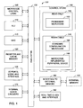
- a microcontroller core 100 of a microcontroller in accordance with the present invention provides a scalar, microcoded CPU (central processing unit).
- the core includes microcode control logic 105, an ALU (arithmetic logic unit) 110, a MAC (multiply-accumulate unit) 115, and local operand storage in a register and cache memory 120.
- the MAC 115 is available to any microcode instruction and can execute an 8x8-bit multiply-add operation in a single microcode instruction. It has an accumulator 19 bits wide to store the extended results of iterative operations.
- the core also includes logic, circuitry and ports 125 to form the I/O (input output) interface of the core. The ports will generally be connected to I/O pins in a packaged integrated circuit product.
- the microcode of the microcontroller core 100 is executed from a control store 140 made up of rewritable memory 144 and non-volatile ROM (read-only memory) 142.
- the rewritable portion 144 of the control store 140 can be implemented in on-chip SRAM (static random access memory) or DRAM (dynamic random access memory).
- the core has a memory interface 150 to memory 155 external to the core, which external memory can be on-chip or off-chip.
- a suitable interface 150 is described in commonly-owned copending PCT application serial number PCT/SE99/01923, designating the United States of America, for "Controlling Access to a Primary Memory” to Sven Stefan Blixt and Björn Stefan Christian Blixt, filed on October 25, 1999, and its priority Swedish patent application serial number SE9803708-8 for "Controlling Access to a Dynamic Random Access Memory", to Sven Stefan Blixt, filed on October 28, 1998, which are incorporated herein by reference.
- Real time clock functions can be provided by a real time clock and interface circuitry 160. If used, this real time clock is driven by an external quartz resonator, such as a 32768 Hz resonator, and supported by battery backup.
- an external quartz resonator such as a 32768 Hz resonator
- the core also includes an on-chip circuitry 170 providing internal clock signals and including a main oscillator and PLL (phase-locked loop) circuitry locked to a reference oscillator that uses an external crystal.
- the main oscillator can provide clock events at an accurate, high frequency, such as 66.667 or 80 MHZ, using a crystal of one quarter of that frequency.
- microcontroller core 100 These and other components of the microcontroller core 100 are interconnected with busses and selectors 130 in a manner conventional to microcoded CPUs. Designed for low-power operation, the data pathways of the microcontroller core 100 are generally 8 bits wide, as are the registers.
- Standard configuration microcode for the microcontroller core includes permanent microcode 143, which is stored in the read-only portion 142 of the control store 140.
- the control store 140 has 36 kilobytes of on-chip ROM and 18 kilobytes of on-chip SRAM.
- the control store is organized into words matching the length of the microcode instructions (which are also called microinstructions).
- a boot loader implemented in the permanent microcode 143 loads the rewritable portion 146 of the standard configuration microcode, typically from an off-chip source such as flash memory connected to programmable I/O port pins of the I/O logic and interface circuitry 125. After the microcontroller boots itself and initializes memory, more microcode can be loaded from the same or other sources.
- This sequence allows customized or patched microcode to reside in a connected device or elsewhere. This sequence will load that part of the standard configuration of microcode for the microcontroller core 100 that was not included in the read-only portion 142 of the control store 140.
- the microcode loaded into the rewritable portion 144 at any stage can include microcode 148 for peripheral devices implemented in microcode, which will be described below.
- an application program can use a special assembly-language instruction to load fresh microcode at any time, which allows applications to alter the macro instruction set of the microcontroller on the fly.
- the microcontroller core 100 is designed to be implemented, and is implemented, on a single monolithic semiconductor substrate.
- the memory on board the microcontroller chip can optionally include memory for application software and data.
- microcode instructions are decoded by the microcode control logic 105 to produce various control signals that are passed to the different functional elements of the core.
- the elements of the core perform operations such as multiplication, addition, shifting, and logical operations.
- the microcode instruction has a long instruction word format ⁇ in the present implementation, it is 72 bits wide ⁇ and can cause the core to perform numerous operations in parallel, including selecting the next microinstruction to be executed.
- the register and cache memory 120 provides storage for use by the microcode. This memory is used, for example, to provide register storage for register-based macro instructions and stack storage for stack-based macro instructions. It can be implemented in 1 kilobyte of SRAM, with stack overflow to an external memory such as memory 155.
- Macro instructions are implemented as microprograms, i.e., as sequences of one or more microcode instructions.
- Microcode sequence control (sometimes called flow control) is controlled by fields of the microinstruction, where one field selects a kind of jump, for example, and another field selects a condition for that jump.
- the microcontroller core 100 has several types of multiway jumps. One type is a table jump, which decodes combinations of condition flip-flops in the arithmetic unit. Another type is a decode jump that decodes an 8-bit macro instruction opcode (whether read either directly from memory or from an instruction register IR) and jumps into a 256-word decode table.
- a microinstruction sets up all the control signals for the logic in the microcontroller, so that data flows into the ALU, the MAC, and other processing units, and so that these units do the required processing operation on the data flowing into them and output the results, which then flow to the destinations specified by the microinstruction. This includes the calculation of the next microinstruction address.
- a microinstruction execution time ends at the rising edge of an execute clock signal, which loads the new state in the processor. Thus, a microinstruction executes and, simultaneously, fetches the next microinstruction.
- FIG. 2 illustrates the relevant aspects of flow control in the microcontroller core.
- the illustration begins with a series of conditional-jump boxes 202-210, which are drawn directly together to indicate that they are actually not performed sequentially.
- the tests illustrated by the conditional-jump boxes 202-210 are performed in hardware by a priority encoder, and they are done simultaneously with, and as part of the execution of, the last microinstruction of the execution sequence for each macro instruction opcode.
- opcode sequences 230 There are approximately as many sequences as there are opcodes, and they are illustrated in the aggregate as opcode sequences 230. For multiple macro instruction sets, partial or entire sets of alternative sequences 230 are implemented. Each sequence starts in a slot in a decode table of 256 microinstructions.
- the conditional-jump blocks 202-210 represent the multiway jump made in the last microinstruction of each execution sequence. Each jump is made to a micro instruction contained in a fetch table.
- the normal flow is to the fetch table microinstruction 220, which performs a number of actions including a decode jump that gives control to one of the 256 instructions in a 256-entry decode table, which is part of the opcode sequences 230, according to the current macro instruction opcode.
- a microinstruction need only change the current fetch table, which changes the current decode table. In principal, any number of fetch tables, and therefore any number of instruction sets, can be created.
- the multiway jump represented by boxes 202-210 is a jump into the current fetch table.
- the least significant bits of the jump address are generated by a priority encoder, the inputs to which come from several different sources, including an internal time interrupt request signal and two external interrupt request signals, NMI (non-maskable interrupt) and IRQ (interrupt request).
- NMI non-maskable interrupt
- IRQ interrupt request
- the IRQ condition causes a jump to a microcode sequence that identifies and acknowledges the external request and sets a flag in an interrupt register IRR, which is simply a reserved area of memory, such as external memory 155 (FIG. 1).
- the NMI condition executes microcode tasks requiring high-priority interrupt service.
- the time interrupt performs a number of services, which will be described later.
- a microcode sequence can exit in one of a number of alternative ways. For example, opcode sequences that need to be chained to the next macro instruction without the possibility of an intervening interrupt exit to the fetch table instruction 220, bypassing the conditional-jump blocks 202-210 (flow path 225).
- a sequence can also be programmed to suspend its processing by calling a sense routine 235, which performs its function and then returns to continue execution of the sequence that called it.
- the sense routine is used in the execution of opcodes that require very long execution time. Its main purpose is to check and service the time interrupt signal, so that every such request will get guaranteed service before the next one arrives, which is the same service provided in response to a time interrupt signal at jump box 204. This interrupt occurs at a sufficiently high frequency, such as 16 kHz or greater, to allow the scheduled tasks to provide real-time services.
- the time service includes doing as many DRAM refresh cycles as are needed, if the microcontroller has, or is connected to, DRAM memory. It also includes adding a time increment to a time accumulator in memory, incrementing a milliseconds counter (also in memory) if it overflows, and updating the memory cells containing the time-of-day when the millisecond counter indicates this should be done. When these fixed tasks have been performed, the microcontrol program continues and performs other scheduled tasks.
- the scheduled tasks can be configured to perform the functions of peripheral devices. For example, they can stream data (through a DMA buffer memory) to a print engine, or from a scanner engine, or to or from an external communications device. Separately or as part of the process of streaming data, scheduled tasks can also provide filtering functions, or compression/decompression functions, that act on such data streams that pass between I/O devices and memory, or from memory to memory, or from input device to output device. These functions can be performed by scheduled tasks because microinstructions have access to all of the processing resources of the microcontroller, including the MAC, and all data transfers within the microcontroller are performed by microcode.
- a basic peripheral device function ⁇ from which numerous other functions can be built ⁇ is a timer function.
- This function can be performed by a scheduled task (i.e., a microcode sequence) that increments or decrements a counter value in memory and detects whether it reaches predefined number such as zero. If so, the timer function performs an action that is specified by one or more device control parameters stored in memory.
- the memory cells containing the parameters belong to a scheduled instantiation of this type of timer.
- Several timers of the same type using common microcode can be scheduled. Shared microcode for common standard types can optionally be included in the ROM microcode 143. Timers can be chained to each other through control parameters.
- Timers can have parameters for start values and have actions like writing "1" or "0" to an output pin selected by parameter. In this way a pair of timers can generate a pulse train with specified frequency and duty cycle. Combinations of such pulsed signals, with specified phase and/or frequency relations, can readily be defined for purposes such as driving a stepper motor or a display.
- the device control parameters can be organized with other data in a controlling data structure (a control block).
- a controlling data structure a control block
- the initial state of a periodic pulse train signal can be defined in a control block as having any phase, so that a pair of such signals driving a stepper motor has the proper phase difference.
- the control block can also contain a total number of counts that is copied to a count variable when that variable has reached zero.
- an accumulator value can be used that is never restarted by loading a fixed value, but instead is increased each time by a fixed value (not simply 1) and the specified action is taken when the accumulator overflows.
- An action specified for a timer can set an interrupt request in a specified bit position in an interrupt register IRR, for example, or otherwise set a condition that will be treated by the microcontroller core like a hardware interrupt from a hardware device.
- timer function can also be to generate a general reset of the processor, as in a watchdog function.
- a timer must be restarted by the software at some minimum frequency; if the program derails or hangs, the watchdog will cause a restart of the system.
- the scheduling can be controlled by a data structure in a memory such as memory 155.
- the data structure can be created and modified by software such as a development system, described below, and can be organized in a data structure such as an ordered list of elements.
- the elements would be accessed and acted upon, one by one in order, by a scheduled task in the time interrupt service microcode.
- Each element describes one task.
- Elements can optionally have a variable size according to the number of parameters the corresponding specific task type needs.
- the microprogram can act on any requests that have been generated by the tasks and then return to normal instruction execution.
- scheduled tasks can be used to implement microcode-implemented peripheral devices.
- the scheduling of tasks that implement such virtual devices can be done using a table in a memory to list the device tasks in the order in which they are to be executed.
- the table identifies the virtual device by its microprogram start address (or an address surrogate) and includes the device parameters.
- the start address can be in ROM 142 or RAM 144.
- the device microcode can share control store space by using common microinstruction subroutines.
- a development system is used by one or more program developers to create programming for the microcontroller core.
- the development system is a conventional integrated environment running on a general purpose platform, such as a personal computer running the Microsoft Windows 98 operating system, providing programming and debugging tools through a graphical user interface.
- the development system includes assemblers and compilers for developing and debugging software on all programming levels.
- a manufacturer of a microcontroller device will provide the microcode for one or more instruction sets ⁇ such as a CISC (Complex Instruction Set Computer) instruction set and a Java Virtual Machine bytecode instruction set ⁇ and control microcode to manage service tasks and generally handle housekeeping functions.
- microcontrollers With conventional microcontrollers, a customer would typically buy a version of the microcontroller configured with the peripheral devices needed by the customer's application and then provide the programming for that application.
- the application programming is generally done in assembly or a higher-level language using a development system provided by the microcontroller vendor.
- the vendor need not provide separate versions with separate configurations of peripheral devices. Instead, the vendor, customer, or a third party can provide microcode 148 implementing the peripheral devices desired by the customer. This is then loaded into the rewritable control store 144 along with the standard microcode 146 for the microcontroller core 100, to provide a microcontroller or microcontroller core configured with the peripheral devices desired by the customer.
- Scenix Semiconductors offers devices, such as low-cost Bell modems, that are based on virtual software peripherals.
- the Scenix solution is based on combination of a fast pipelined RISC (Reduced Instruction Set Computer) processor and a fast on-chip memory. This means that the peripherals axe implemented by the ISA instructions of the RISC processor, and not by microcode as proposed by the invention. In fact, there is no microcode level in a RISC architecture.
- RISC Reduced Instruction Set Computer
- FIG. 3 illustrates one way a programmer can create a microcode-implemented device.
- the operational functionality of the device is identified (step 305) by identifying functions that can each be performed by a sequence of microcode instructions.
- the hardware interface elements of the microcontroller core that will be used as the external interface, if any, for the microcode-implemented device must also be identified (step 310). These will be selected from among the I/O ports and related logic and interface circuitry 125 (FIG. 1) of the core according to availability and suitability.
- Memory and/or core registers also have to be identified for use by the modules implementing the device (step 315).
- the programmer can use any of the resources of the core not already used by the manufacturer or the customer's vendor.
- the programmer then writes microcode-device modules to perform the operational functions and interact with the interface hardware, if any, and the programmatic interface of the microcode-implemented device (step 320).
- the programmer may also provide a device initialization module (step 330) to be executed by the microcontrol program of the microcontroller core at initialization time, to initialize any resources reserved for use by the device and to enqueue any initial modules for execution.
- a suite of one or more microcode-device modules implementing the peripheral device are added to a microcode file that will be read into the rewritable portion of the control store (step 405).
- a module may include microcode instructions or device control data. If a module is simply device control data, such as a table entry including a control store address and device control parameters, as described above, the module can and generally will be read into some other memory, such as external memory 155, for use by microcode instructions implementing a service task.
- the file is loaded into the control store, which loads the microcode-implemented device (step 410). Any device initialization module is recognized and executed by the microcontrol program (step 415). The microcontrol program then executes the modules of the microcode-implemented peripheral device as a service task, as has been described (step 420).
- a pulse generator can be built from two basic timer devices.
- the timers are of a type that count up or down at each time interrupt until they reach the end, and then do their action and stop in an end state. The action changes the signal on an output pin and starts another timer of the same kind by initializing its counter.
- the microcode-device module specifies microcode instructions for a complete pulse generator type of device, having a state bit keeping track of its state (high or low) and two initialization constants. This is a repetitive type of device that would not stop when at the end count, but instead reinitialize itself in the opposite state. With a third basic timer device or with a pulse generator device maintaining a third pin state, a pulse train with a third level can be produced.
- each of these types of devices can use the other, more accurate way of counting, described above, in which an accumulator is incremented without reset by an appropriately selected value.
- a higher level pattern generator device can be built to generate patterns of pulse trains, and data transfers can be coupled to the generated pulses.
- Stepper motors for example, need pulse signals that have variable frequency and phase.
- Audio tones can be produced by pulse-width modulation by a sinusoidal signal: the service task for the virtual audio device can fetch the required data from a table in memory 155.
- the microcontroller core is configured with an optional hardware counter.
- This counter can be started by a microcode instruction loading it with a non-zero value. Once started it counts pulses derived from the main oscillator. When it reaches zero it stops counting and causes a high-priority hardware interrupt request, such as request 202 (FIG. 1) to be set. When this request is detected, a service task similar to the one described for the time interrupt tick is invoked. There, actions specified for a trailing pulse edge are executed.
- More than one narrow-width pulse generator device can be supported if needed. Because the counter is used for short pulses that are started at time ticks, one can assume that it will always have reached zero and is inactivate when the time interrupt service task is executed. If the schedule for service tasks includes narrow-width pulse generator devices, each one of will have its companion trailing edge device scheduled in another, trailing-edge list that will be used by the high-priority interrupt service microprogram that will follow some microseconds later. When the time request service scheduler finds a narrow-width pulse device, and finds that this device is now in the state when it should perform its leading-edge action, i.e., start its pulse (and do some data transfer if specified), the microprogram will do that.
- the microprogram copies a device-identifier byte that identifies the device to a device-identifier location, and copies one of the device's parameters (the pulse width measured in counter clock pulses) into the counter ⁇ however, it will not do these two actions if the counter already contains a nonzero value smaller than or equal to the pulse width parameter. This can happen an narrow-pulse device earlier in the list starts its pulse on the same time interrupt tick.
- the microprogram indicates this very special situation with a special marker bit in memory, in a way that is easy for the high-priority interrupt service microprogram to detect.
- the high-priority interrupt service microprogram is invoked when the counter reaches zero. It will read the device-identifier location, thereby identifying the pulse-starting device (or one of them), and perform that device's parameter-specified trailing edge actions and eliminate its active-pulse state indication. If the special marker bit is set, it will search for all devices having an active pulse state, selecting the one with the lowest value of pulse width, and load the counter with the difference between that pulse width and that of the device just serviced. If the difference is zero it will do the actions for the found device also, and find a new one with the lowest pulse width, and so on. This way several pulses with same or different pulse width can be allowed to overlap and be independent from each other.
- Virtual devices can be used to implement LCD (liquid crystal display) driving that is configurable and can accept many different LCD types.
- a bigger graphic LCD normally needs parallel input data, a clock signal to clock in the data and control the scanning (stepping from a pixel to the next in a color or grayscale device, or stepping from 8 pixels to the next 8 pixels in a bilevel monochrome device), and frame or synch signals for the synchronization of the phase of the scanning process to the input data.
- Some scanner sensors and print engines need the same kinds of signals.
- the required signals can be provided by microcoded repetitive pulse generators having parameters giving them different frequencies, can be coupled by specialized actions to provide a pattern of dot clock, line synch (horizontal synch), and frame synch (vertical synch).
- the dot clock (or at least the data transfer) should be inhibited for some time between lines and/or frames.
- Such effects can be accomplished by a hierarchical (tree) structure for the scheduling, allowing one virtual device to control (enable/disable) another, lower-level, virtual device.
- Another example application is to key switches, which are normally connected in a matrix of row and column lines. Depressing a key connects one row line to one column line. Microcontroller ports can be used to drive one set of lines, e.g. rows, while sensing the other set. A 4 x 5 key matrix thus requires 4 output ports and 5 input ports (or vice versa).
- Such a keypad can be scanned in the following way, for the case of 4 output ports.
- Another example application implements a method of automatically transferring parts of several bitmap images from memory to an LCD, such that one can select viewports in the memory image areas and divide the LCD screen into windows.
- a viewport-window pair defines a copy transformation from memory to LCD. These transformations are specified in a table in memory.
- the LCD has to be refreshed (scanned) at a steady rate, which generally gives a frame frequency of about 80 Hz.
- the automatic transfer service task fetches data in the memory, it increments its memory pointer for the data in order to fetch the next data next time. It also checks, by a simple countdown, whether it has reached the right-hand edge of the window it is writing into. If so, it will look in a table to find the viewport and starting source address it should use at the point (a left edge) in the window it is entering. It also loads the count value corresponding to the width of this window. In this way multiple windows can be implemented, the contents of which will scroll "softly", scan line by scan line or pixel column by pixel column, without moving data in the memory. Soft-scrolling lists on display on a mobile telephone, for example, is useful because it is easier for the eye to follow it can be done with little more than changing a few parameters in a window definition table (instead of moving bitmaps in memory).
- a line table format that can be used to define the windows on a screen in a way that can be used by such a method has five columns.
- the microcontroller core can be configured with special purpose circuitry for loading microcode instructions into a rewritable control store, in which case the entire control store can be rewritable.
- the microcontroller core can be configured with modules of microcode-device instructions in a read-only control store, and virtual devices can be implemented solely by appropriate definition of control blocks defining fundamental functions such as timers.
- control blocks or device control data can be organized using a data structure such as a linked list or a tree that can be navigated by a service task implemented in read-only control store to implement the virtual devices defined by the device control data.
- the design of the microcontroller core can be represented in a synthesizable HDL (hardware description language) description, such as a VHDL description (VHSIC (Very High Speed Integrated Circuits) HDL.
- VHSIC Very High Speed Integrated Circuits
Landscapes
- Engineering & Computer Science (AREA)
- Software Systems (AREA)
- Theoretical Computer Science (AREA)
- Physics & Mathematics (AREA)
- General Engineering & Computer Science (AREA)
- General Physics & Mathematics (AREA)
- Computer Security & Cryptography (AREA)
- Microcomputers (AREA)
- Executing Machine-Instructions (AREA)
Applications Claiming Priority (2)
| Application Number | Priority Date | Filing Date | Title |
|---|---|---|---|
| US429748 | 1989-10-30 | ||
| US09/429,748 US7103759B1 (en) | 1999-10-28 | 1999-10-28 | Microcontroller architecture supporting microcode-implemented peripheral devices |
Publications (3)
| Publication Number | Publication Date |
|---|---|
| EP1096370A2 true EP1096370A2 (de) | 2001-05-02 |
| EP1096370A3 EP1096370A3 (de) | 2004-05-06 |
| EP1096370B1 EP1096370B1 (de) | 2005-08-10 |
Family
ID=23704580
Family Applications (1)
| Application Number | Title | Priority Date | Filing Date |
|---|---|---|---|
| EP00122984A Expired - Lifetime EP1096370B1 (de) | 1999-10-28 | 2000-10-23 | Mikrokontrollerarchitektur mit mikrocodierten Peripheriegeräten |
Country Status (4)
| Country | Link |
|---|---|
| US (1) | US7103759B1 (de) |
| EP (1) | EP1096370B1 (de) |
| AT (1) | ATE301848T1 (de) |
| DE (1) | DE60021827T2 (de) |
Families Citing this family (11)
| Publication number | Priority date | Publication date | Assignee | Title |
|---|---|---|---|---|
| US6976239B1 (en) * | 2001-06-12 | 2005-12-13 | Altera Corporation | Methods and apparatus for implementing parameterizable processors and peripherals |
| US7305567B1 (en) * | 2002-03-01 | 2007-12-04 | Cavium Networks, In. | Decoupled architecture for data ciphering operations |
| US20080209076A1 (en) * | 2007-02-22 | 2008-08-28 | Wei Wang | Method and system for fast ethernet controller operation using a virtual cpu |
| US8438549B1 (en) * | 2009-09-15 | 2013-05-07 | Sandia Corporation | Data processing with microcode designed with source coding |
| US11797474B2 (en) * | 2011-02-17 | 2023-10-24 | Hyperion Core, Inc. | High performance processor |
| CN103489432B (zh) * | 2013-08-30 | 2016-04-13 | 小米科技有限责任公司 | 电子设备及资源显示方法 |
| CN108595147B (zh) * | 2018-01-02 | 2021-03-23 | 上海兆芯集成电路有限公司 | 具有级数运算执行电路的微处理器 |
| DE102018115203B3 (de) | 2018-06-25 | 2019-09-19 | Hyundai Autron Co., Ltd. | Multi-master-system, leistungssteuereinrichtung und verfahren zum betreiben des multi-master-systems |
| US10994718B2 (en) | 2018-06-27 | 2021-05-04 | Hyundai Autron Co., Ltd. | Multi-master system, power controller and operating method of the multi-master system |
| CN113162585B (zh) * | 2021-04-02 | 2023-02-17 | 浙江清华柔性电子技术研究院 | 脉冲控制方法、装置及电子设备 |
| CN114579483B (zh) * | 2022-03-02 | 2023-07-04 | 北京超智芯科技有限公司 | 一种基于软件实现外设的sdp芯片及方法 |
Family Cites Families (7)
| Publication number | Priority date | Publication date | Assignee | Title |
|---|---|---|---|---|
| US3478322A (en) * | 1967-05-23 | 1969-11-11 | Ibm | Data processor employing electronically changeable control storage |
| US3735363A (en) * | 1971-04-07 | 1973-05-22 | Burroughs Corp | Information processing system employing stored microprogrammed processors and access free field memories |
| DE69230642T2 (de) * | 1991-11-12 | 2001-05-23 | Microchip Technology Inc., Chandler | Automatischer programmierungs-mikrokontroller mit gespeichertem befehl zur programm-steuerung von externem speicher und verfahren |
| FR2700402B1 (fr) * | 1993-01-13 | 1995-04-07 | Sgs Thomson Microelectronics | Microcontrôleur à mémoire électriquement programmable multimode. |
| US5781750A (en) | 1994-01-11 | 1998-07-14 | Exponential Technology, Inc. | Dual-instruction-set architecture CPU with hidden software emulation mode |
| GB2307072B (en) | 1994-06-10 | 1998-05-13 | Advanced Risc Mach Ltd | Interoperability with multiple instruction sets |
| US5481693A (en) | 1994-07-20 | 1996-01-02 | Exponential Technology, Inc. | Shared register architecture for a dual-instruction-set CPU |
-
1999
- 1999-10-28 US US09/429,748 patent/US7103759B1/en not_active Expired - Lifetime
-
2000
- 2000-10-23 EP EP00122984A patent/EP1096370B1/de not_active Expired - Lifetime
- 2000-10-23 DE DE60021827T patent/DE60021827T2/de not_active Expired - Lifetime
- 2000-10-23 AT AT00122984T patent/ATE301848T1/de not_active IP Right Cessation
Also Published As
| Publication number | Publication date |
|---|---|
| DE60021827D1 (de) | 2005-09-15 |
| US7103759B1 (en) | 2006-09-05 |
| EP1096370A3 (de) | 2004-05-06 |
| ATE301848T1 (de) | 2005-08-15 |
| DE60021827T2 (de) | 2006-03-16 |
| EP1096370B1 (de) | 2005-08-10 |
Similar Documents
| Publication | Publication Date | Title |
|---|---|---|
| US4878174A (en) | Flexible ASIC microcomputer permitting the modular modification of dedicated functions and macroinstructions | |
| US9003422B2 (en) | Microprocessor architecture having extendible logic | |
| EP1096370B1 (de) | Mikrokontrollerarchitektur mit mikrocodierten Peripheriegeräten | |
| US8135975B2 (en) | Software programmable timing architecture | |
| US20030101440A1 (en) | Multiple virtual machine environment management system | |
| US7930443B1 (en) | Router having routing engine software instance and interface controller software instance on a single processor | |
| EP0740254A2 (de) | Mikroprozessor und Verfahren zur Aufstellung seiner Peripheriefunktionen | |
| EP0614550A1 (de) | Automatischer programmierungs-mikrokontroller mit gespeichertem befehl zur programm-steuerung von externem speicher | |
| US5155819A (en) | Flexible ASIC microcomputer permitting the modular modification of dedicated functions and macroinstructions | |
| KR100381074B1 (ko) | 데이타처리시스템및데이타프로세서구성방법 | |
| US5623687A (en) | Reset configuration in a data processing system and method therefor | |
| US5455937A (en) | Microcontroller with fuse-emulating latches | |
| US5046040A (en) | Microprogram control apparatus using don't care bits as part of address bits for common instructions and generating variable control bits | |
| US20030009655A1 (en) | System and method for data processing system initialization | |
| US5606715A (en) | Flexible reset configuration of a data processing system and method therefor | |
| JP2002152020A (ja) | パルス信号生成装置 | |
| KR100557518B1 (ko) | 시스템 대규모 집적 회로, 그 설계 방법, 및 그에 대한프로그램 | |
| EP0907124A1 (de) | Mikrocomputer und elektronische ausrüstung | |
| EP0875836A2 (de) | RISC-basierter Microcontroller mit an einem geteilten Datenbus zugefügter Peripheriefunktion | |
| JPS6230452B2 (de) | ||
| JP2002297376A (ja) | プログラマブルコントローラ | |
| JPH087608B2 (ja) | パルス出力装置 | |
| JPH09244918A (ja) | デバッガ付きインタプリタへの機能付加方式 | |
| JP2000148511A (ja) | マイクロコンピュータの割り込み処理装置および割り込み処理方法 | |
| JPH0492925A (ja) | 中央処理装置 |
Legal Events
| Date | Code | Title | Description |
|---|---|---|---|
| PUAI | Public reference made under article 153(3) epc to a published international application that has entered the european phase |
Free format text: ORIGINAL CODE: 0009012 |
|
| AK | Designated contracting states |
Kind code of ref document: A2 Designated state(s): AT BE CH CY DE DK ES FI FR GB GR IE IT LI LU MC NL PT SE |
|
| AX | Request for extension of the european patent |
Free format text: AL;LT;LV;MK;RO;SI |
|
| PUAL | Search report despatched |
Free format text: ORIGINAL CODE: 0009013 |
|
| AK | Designated contracting states |
Kind code of ref document: A3 Designated state(s): AT BE CH CY DE DK ES FI FR GB GR IE IT LI LU MC NL PT SE |
|
| AX | Request for extension of the european patent |
Extension state: AL LT LV MK RO SI |
|
| RAP1 | Party data changed (applicant data changed or rights of an application transferred) |
Owner name: IMSYS TECHNOLOGIES AB |
|
| 17P | Request for examination filed |
Effective date: 20041007 |
|
| AKX | Designation fees paid |
Designated state(s): AT BE CH CY DE DK ES FI FR GB GR IE IT LI LU MC NL PT SE |
|
| GRAP | Despatch of communication of intention to grant a patent |
Free format text: ORIGINAL CODE: EPIDOSNIGR1 |
|
| GRAS | Grant fee paid |
Free format text: ORIGINAL CODE: EPIDOSNIGR3 |
|
| GRAA | (expected) grant |
Free format text: ORIGINAL CODE: 0009210 |
|
| AK | Designated contracting states |
Kind code of ref document: B1 Designated state(s): AT BE CH CY DE DK ES FI FR GB GR IE IT LI LU MC NL PT SE |
|
| PG25 | Lapsed in a contracting state [announced via postgrant information from national office to epo] |
Ref country code: AT Free format text: LAPSE BECAUSE OF FAILURE TO SUBMIT A TRANSLATION OF THE DESCRIPTION OR TO PAY THE FEE WITHIN THE PRESCRIBED TIME-LIMIT Effective date: 20050810 Ref country code: ES Free format text: LAPSE BECAUSE OF FAILURE TO SUBMIT A TRANSLATION OF THE DESCRIPTION OR TO PAY THE FEE WITHIN THE PRESCRIBED TIME-LIMIT Effective date: 20050810 Ref country code: CH Free format text: LAPSE BECAUSE OF FAILURE TO SUBMIT A TRANSLATION OF THE DESCRIPTION OR TO PAY THE FEE WITHIN THE PRESCRIBED TIME-LIMIT Effective date: 20050810 Ref country code: FI Free format text: LAPSE BECAUSE OF FAILURE TO SUBMIT A TRANSLATION OF THE DESCRIPTION OR TO PAY THE FEE WITHIN THE PRESCRIBED TIME-LIMIT Effective date: 20050810 Ref country code: NL Free format text: LAPSE BECAUSE OF FAILURE TO SUBMIT A TRANSLATION OF THE DESCRIPTION OR TO PAY THE FEE WITHIN THE PRESCRIBED TIME-LIMIT Effective date: 20050810 Ref country code: BE Free format text: LAPSE BECAUSE OF FAILURE TO SUBMIT A TRANSLATION OF THE DESCRIPTION OR TO PAY THE FEE WITHIN THE PRESCRIBED TIME-LIMIT Effective date: 20050810 Ref country code: LI Free format text: LAPSE BECAUSE OF FAILURE TO SUBMIT A TRANSLATION OF THE DESCRIPTION OR TO PAY THE FEE WITHIN THE PRESCRIBED TIME-LIMIT Effective date: 20050810 Ref country code: IT Free format text: LAPSE BECAUSE OF FAILURE TO SUBMIT A TRANSLATION OF THE DESCRIPTION OR TO PAY THE FEE WITHIN THE PRESCRIBED TIME-LIMIT;WARNING: LAPSES OF ITALIAN PATENTS WITH EFFECTIVE DATE BEFORE 2007 MAY HAVE OCCURRED AT ANY TIME BEFORE 2007. THE CORRECT EFFECTIVE DATE MAY BE DIFFERENT FROM THE ONE RECORDED. Effective date: 20050810 |
|
| REG | Reference to a national code |
Ref country code: GB Ref legal event code: FG4D |
|
| REG | Reference to a national code |
Ref country code: CH Ref legal event code: EP |
|
| REG | Reference to a national code |
Ref country code: IE Ref legal event code: FG4D |
|
| REF | Corresponds to: |
Ref document number: 60021827 Country of ref document: DE Date of ref document: 20050915 Kind code of ref document: P |
|
| PG25 | Lapsed in a contracting state [announced via postgrant information from national office to epo] |
Ref country code: CY Free format text: LAPSE BECAUSE OF FAILURE TO SUBMIT A TRANSLATION OF THE DESCRIPTION OR TO PAY THE FEE WITHIN THE PRESCRIBED TIME-LIMIT Effective date: 20051023 |
|
| PG25 | Lapsed in a contracting state [announced via postgrant information from national office to epo] |
Ref country code: IE Free format text: LAPSE BECAUSE OF NON-PAYMENT OF DUE FEES Effective date: 20051024 |
|
| PG25 | Lapsed in a contracting state [announced via postgrant information from national office to epo] |
Ref country code: MC Free format text: LAPSE BECAUSE OF NON-PAYMENT OF DUE FEES Effective date: 20051031 Ref country code: LU Free format text: LAPSE BECAUSE OF NON-PAYMENT OF DUE FEES Effective date: 20051031 |
|
| PG25 | Lapsed in a contracting state [announced via postgrant information from national office to epo] |
Ref country code: DK Free format text: LAPSE BECAUSE OF FAILURE TO SUBMIT A TRANSLATION OF THE DESCRIPTION OR TO PAY THE FEE WITHIN THE PRESCRIBED TIME-LIMIT Effective date: 20051110 Ref country code: GR Free format text: LAPSE BECAUSE OF FAILURE TO SUBMIT A TRANSLATION OF THE DESCRIPTION OR TO PAY THE FEE WITHIN THE PRESCRIBED TIME-LIMIT Effective date: 20051110 Ref country code: SE Free format text: LAPSE BECAUSE OF FAILURE TO SUBMIT A TRANSLATION OF THE DESCRIPTION OR TO PAY THE FEE WITHIN THE PRESCRIBED TIME-LIMIT Effective date: 20051110 |
|
| PG25 | Lapsed in a contracting state [announced via postgrant information from national office to epo] |
Ref country code: PT Free format text: LAPSE BECAUSE OF FAILURE TO SUBMIT A TRANSLATION OF THE DESCRIPTION OR TO PAY THE FEE WITHIN THE PRESCRIBED TIME-LIMIT Effective date: 20060110 |
|
| NLV1 | Nl: lapsed or annulled due to failure to fulfill the requirements of art. 29p and 29m of the patents act | ||
| REG | Reference to a national code |
Ref country code: CH Ref legal event code: PL |
|
| ET | Fr: translation filed | ||
| PLBE | No opposition filed within time limit |
Free format text: ORIGINAL CODE: 0009261 |
|
| STAA | Information on the status of an ep patent application or granted ep patent |
Free format text: STATUS: NO OPPOSITION FILED WITHIN TIME LIMIT |
|
| 26N | No opposition filed |
Effective date: 20060511 |
|
| REG | Reference to a national code |
Ref country code: IE Ref legal event code: MM4A |
|
| REG | Reference to a national code |
Ref country code: GB Ref legal event code: 732E Free format text: REGISTERED BETWEEN 20100408 AND 20100414 |
|
| REG | Reference to a national code |
Ref country code: FR Ref legal event code: TQ |
|
| REG | Reference to a national code |
Ref country code: DE Ref legal event code: R082 Ref document number: 60021827 Country of ref document: DE Representative=s name: MOSER GOETZE & PARTNER PATENTANWAELTE MBB, DE Ref country code: FR Ref legal event code: PLFP Year of fee payment: 16 Ref country code: DE Ref legal event code: R081 Ref document number: 60021827 Country of ref document: DE Owner name: IMSYS AB, SE Free format text: FORMER OWNERS: CONEMTECH AG, KISTA, SE; IMSYS AB, UPPLANDS VAESBY, SE |
|
| REG | Reference to a national code |
Ref country code: GB Ref legal event code: 732E Free format text: REGISTERED BETWEEN 20151217 AND 20151223 |
|
| REG | Reference to a national code |
Ref country code: FR Ref legal event code: CD Owner name: QULSAR SWEDEN AB Effective date: 20160203 Ref country code: FR Ref legal event code: CD Owner name: IMSYS AB, SE Effective date: 20160203 |
|
| REG | Reference to a national code |
Ref country code: FR Ref legal event code: TP Owner name: IMSYS AB, SE Effective date: 20160224 |
|
| REG | Reference to a national code |
Ref country code: FR Ref legal event code: PLFP Year of fee payment: 17 |
|
| REG | Reference to a national code |
Ref country code: FR Ref legal event code: PLFP Year of fee payment: 18 |
|
| REG | Reference to a national code |
Ref country code: FR Ref legal event code: PLFP Year of fee payment: 19 |
|
| PGFP | Annual fee paid to national office [announced via postgrant information from national office to epo] |
Ref country code: DE Payment date: 20181018 Year of fee payment: 19 |
|
| PGFP | Annual fee paid to national office [announced via postgrant information from national office to epo] |
Ref country code: FR Payment date: 20181025 Year of fee payment: 19 Ref country code: GB Payment date: 20181010 Year of fee payment: 19 |
|
| REG | Reference to a national code |
Ref country code: DE Ref legal event code: R119 Ref document number: 60021827 Country of ref document: DE |
|
| PG25 | Lapsed in a contracting state [announced via postgrant information from national office to epo] |
Ref country code: DE Free format text: LAPSE BECAUSE OF NON-PAYMENT OF DUE FEES Effective date: 20200501 |
|
| GBPC | Gb: european patent ceased through non-payment of renewal fee |
Effective date: 20191023 |
|
| PG25 | Lapsed in a contracting state [announced via postgrant information from national office to epo] |
Ref country code: GB Free format text: LAPSE BECAUSE OF NON-PAYMENT OF DUE FEES Effective date: 20191023 Ref country code: FR Free format text: LAPSE BECAUSE OF NON-PAYMENT OF DUE FEES Effective date: 20191031 |