EP1104059A2 - Struktur und Verfahren für indexgeführten internen Streifendiodenlaser - Google Patents
Struktur und Verfahren für indexgeführten internen Streifendiodenlaser Download PDFInfo
- Publication number
- EP1104059A2 EP1104059A2 EP00309746A EP00309746A EP1104059A2 EP 1104059 A2 EP1104059 A2 EP 1104059A2 EP 00309746 A EP00309746 A EP 00309746A EP 00309746 A EP00309746 A EP 00309746A EP 1104059 A2 EP1104059 A2 EP 1104059A2
- Authority
- EP
- European Patent Office
- Prior art keywords
- layer
- current blocking
- blocking layer
- stripe
- wave guide
- Prior art date
- Legal status (The legal status is an assumption and is not a legal conclusion. Google has not performed a legal analysis and makes no representation as to the accuracy of the status listed.)
- Granted
Links
Images


Classifications
-
- B—PERFORMING OPERATIONS; TRANSPORTING
- B82—NANOTECHNOLOGY
- B82Y—SPECIFIC USES OR APPLICATIONS OF NANOSTRUCTURES; MEASUREMENT OR ANALYSIS OF NANOSTRUCTURES; MANUFACTURE OR TREATMENT OF NANOSTRUCTURES
- B82Y20/00—Nanooptics, e.g. quantum optics or photonic crystals
-
- H—ELECTRICITY
- H01—ELECTRIC ELEMENTS
- H01S—DEVICES USING THE PROCESS OF LIGHT AMPLIFICATION BY STIMULATED EMISSION OF RADIATION [LASER] TO AMPLIFY OR GENERATE LIGHT; DEVICES USING STIMULATED EMISSION OF ELECTROMAGNETIC RADIATION IN WAVE RANGES OTHER THAN OPTICAL
- H01S5/00—Semiconductor lasers
- H01S5/30—Structure or shape of the active region; Materials used for the active region
- H01S5/34—Structure or shape of the active region; Materials used for the active region comprising quantum well or superlattice structures, e.g. single quantum well [SQW] lasers, multiple quantum well [MQW] lasers or graded index separate confinement heterostructure [GRINSCH] lasers
- H01S5/343—Structure or shape of the active region; Materials used for the active region comprising quantum well or superlattice structures, e.g. single quantum well [SQW] lasers, multiple quantum well [MQW] lasers or graded index separate confinement heterostructure [GRINSCH] lasers in AIIIBV compounds, e.g. AlGaAs-laser, InP-based laser
- H01S5/34333—Structure or shape of the active region; Materials used for the active region comprising quantum well or superlattice structures, e.g. single quantum well [SQW] lasers, multiple quantum well [MQW] lasers or graded index separate confinement heterostructure [GRINSCH] lasers in AIIIBV compounds, e.g. AlGaAs-laser, InP-based laser with a well layer based on Ga(In)N or Ga(In)P, e.g. blue laser
-
- H—ELECTRICITY
- H01—ELECTRIC ELEMENTS
- H01S—DEVICES USING THE PROCESS OF LIGHT AMPLIFICATION BY STIMULATED EMISSION OF RADIATION [LASER] TO AMPLIFY OR GENERATE LIGHT; DEVICES USING STIMULATED EMISSION OF ELECTROMAGNETIC RADIATION IN WAVE RANGES OTHER THAN OPTICAL
- H01S5/00—Semiconductor lasers
- H01S5/20—Structure or shape of the semiconductor body to guide the optical wave ; Confining structures perpendicular to the optical axis, e.g. index or gain guiding, stripe geometry, broad area lasers, gain tailoring, transverse or lateral reflectors, special cladding structures, MQW barrier reflection layers
- H01S5/22—Structure or shape of the semiconductor body to guide the optical wave ; Confining structures perpendicular to the optical axis, e.g. index or gain guiding, stripe geometry, broad area lasers, gain tailoring, transverse or lateral reflectors, special cladding structures, MQW barrier reflection layers having a ridge or stripe structure
- H01S5/223—Buried stripe structure
- H01S5/2231—Buried stripe structure with inner confining structure only between the active layer and the upper electrode
-
- H—ELECTRICITY
- H01—ELECTRIC ELEMENTS
- H01S—DEVICES USING THE PROCESS OF LIGHT AMPLIFICATION BY STIMULATED EMISSION OF RADIATION [LASER] TO AMPLIFY OR GENERATE LIGHT; DEVICES USING STIMULATED EMISSION OF ELECTROMAGNETIC RADIATION IN WAVE RANGES OTHER THAN OPTICAL
- H01S5/00—Semiconductor lasers
- H01S5/20—Structure or shape of the semiconductor body to guide the optical wave ; Confining structures perpendicular to the optical axis, e.g. index or gain guiding, stripe geometry, broad area lasers, gain tailoring, transverse or lateral reflectors, special cladding structures, MQW barrier reflection layers
- H01S5/22—Structure or shape of the semiconductor body to guide the optical wave ; Confining structures perpendicular to the optical axis, e.g. index or gain guiding, stripe geometry, broad area lasers, gain tailoring, transverse or lateral reflectors, special cladding structures, MQW barrier reflection layers having a ridge or stripe structure
- H01S5/2205—Structure or shape of the semiconductor body to guide the optical wave ; Confining structures perpendicular to the optical axis, e.g. index or gain guiding, stripe geometry, broad area lasers, gain tailoring, transverse or lateral reflectors, special cladding structures, MQW barrier reflection layers having a ridge or stripe structure comprising special burying or current confinement layers
- H01S5/2214—Structure or shape of the semiconductor body to guide the optical wave ; Confining structures perpendicular to the optical axis, e.g. index or gain guiding, stripe geometry, broad area lasers, gain tailoring, transverse or lateral reflectors, special cladding structures, MQW barrier reflection layers having a ridge or stripe structure comprising special burying or current confinement layers based on oxides or nitrides
-
- H—ELECTRICITY
- H01—ELECTRIC ELEMENTS
- H01S—DEVICES USING THE PROCESS OF LIGHT AMPLIFICATION BY STIMULATED EMISSION OF RADIATION [LASER] TO AMPLIFY OR GENERATE LIGHT; DEVICES USING STIMULATED EMISSION OF ELECTROMAGNETIC RADIATION IN WAVE RANGES OTHER THAN OPTICAL
- H01S5/00—Semiconductor lasers
- H01S5/20—Structure or shape of the semiconductor body to guide the optical wave ; Confining structures perpendicular to the optical axis, e.g. index or gain guiding, stripe geometry, broad area lasers, gain tailoring, transverse or lateral reflectors, special cladding structures, MQW barrier reflection layers
- H01S5/22—Structure or shape of the semiconductor body to guide the optical wave ; Confining structures perpendicular to the optical axis, e.g. index or gain guiding, stripe geometry, broad area lasers, gain tailoring, transverse or lateral reflectors, special cladding structures, MQW barrier reflection layers having a ridge or stripe structure
- H01S5/2205—Structure or shape of the semiconductor body to guide the optical wave ; Confining structures perpendicular to the optical axis, e.g. index or gain guiding, stripe geometry, broad area lasers, gain tailoring, transverse or lateral reflectors, special cladding structures, MQW barrier reflection layers having a ridge or stripe structure comprising special burying or current confinement layers
- H01S5/2218—Structure or shape of the semiconductor body to guide the optical wave ; Confining structures perpendicular to the optical axis, e.g. index or gain guiding, stripe geometry, broad area lasers, gain tailoring, transverse or lateral reflectors, special cladding structures, MQW barrier reflection layers having a ridge or stripe structure comprising special burying or current confinement layers having special optical properties
- H01S5/222—Structure or shape of the semiconductor body to guide the optical wave ; Confining structures perpendicular to the optical axis, e.g. index or gain guiding, stripe geometry, broad area lasers, gain tailoring, transverse or lateral reflectors, special cladding structures, MQW barrier reflection layers having a ridge or stripe structure comprising special burying or current confinement layers having special optical properties having a refractive index lower than that of the cladding layers or outer guiding layers
-
- H—ELECTRICITY
- H01—ELECTRIC ELEMENTS
- H01S—DEVICES USING THE PROCESS OF LIGHT AMPLIFICATION BY STIMULATED EMISSION OF RADIATION [LASER] TO AMPLIFY OR GENERATE LIGHT; DEVICES USING STIMULATED EMISSION OF ELECTROMAGNETIC RADIATION IN WAVE RANGES OTHER THAN OPTICAL
- H01S5/00—Semiconductor lasers
- H01S5/20—Structure or shape of the semiconductor body to guide the optical wave ; Confining structures perpendicular to the optical axis, e.g. index or gain guiding, stripe geometry, broad area lasers, gain tailoring, transverse or lateral reflectors, special cladding structures, MQW barrier reflection layers
- H01S5/22—Structure or shape of the semiconductor body to guide the optical wave ; Confining structures perpendicular to the optical axis, e.g. index or gain guiding, stripe geometry, broad area lasers, gain tailoring, transverse or lateral reflectors, special cladding structures, MQW barrier reflection layers having a ridge or stripe structure
- H01S5/2205—Structure or shape of the semiconductor body to guide the optical wave ; Confining structures perpendicular to the optical axis, e.g. index or gain guiding, stripe geometry, broad area lasers, gain tailoring, transverse or lateral reflectors, special cladding structures, MQW barrier reflection layers having a ridge or stripe structure comprising special burying or current confinement layers
- H01S5/2222—Structure or shape of the semiconductor body to guide the optical wave ; Confining structures perpendicular to the optical axis, e.g. index or gain guiding, stripe geometry, broad area lasers, gain tailoring, transverse or lateral reflectors, special cladding structures, MQW barrier reflection layers having a ridge or stripe structure comprising special burying or current confinement layers having special electric properties
- H01S5/2227—Structure or shape of the semiconductor body to guide the optical wave ; Confining structures perpendicular to the optical axis, e.g. index or gain guiding, stripe geometry, broad area lasers, gain tailoring, transverse or lateral reflectors, special cladding structures, MQW barrier reflection layers having a ridge or stripe structure comprising special burying or current confinement layers having special electric properties special thin layer sequence
Definitions
- the invention relates to index guided, inner stripe laser diode structures.
- Inner stripe laser diode structures have been commonly used in both red AlGaInP and infrared AlGaAs laser diodes. Inner stripe laser diode structures provide a convenient means of achieving low threshold, single mode laser diodes.
- An inner stripe laser diode structure requires two epitaxial growth steps. The first epitaxial growth step typically involves growth of the lower cladding layer, the active region, a portion of the upper cladding layer and an n-type blocking layer. Following the etching away of the n-blocking layer in a narrow stripe, the remaining portion of the n-cladding layer is grown. In operation, the injection current path is defined by the etched stripe opening in the n-blocking layer, even though the p-metal contact pad may be significantly wider than the stripe.
- the current-blocking layer is placed close to the active region, typically being at about a 100 - 200 nm separation from the boundary of the active region into the upper-cladding layer. Due to the relative ease of creating a 1 - 2 ⁇ m wide stripe in the n-blocking layer, very low threshold current lasers can be fabricated. It is much easier to form a 2 ⁇ m wide stripe in this self-aligned structure in comparison with, for example, the similarly narrow ridge waveguide laser because a ridge waveguide structure requires that a narrow contact stripe, typically 1-1.5 ⁇ m, be carefully aligned on the top of the ridge structure.
- Very narrow inner stripe laser diodes offer improved heat dissipation because lateral heat spreading is enhanced as the width of the laser stripe is reduced.
- the inner stripe structure is often the first structure used to achieve a single mode laser.
- the inner stripe laser diode structure is advantageous to achieving low threshold, single mode operation, the resulting beam quality is relatively poor and unsuitable for many important applications.
- the beam quality is relatively poor because no lateral positive index guiding is provided by the inner stripe laser diode structure. Instead, a highly astigmatic beam is generated because the inner laser stripe structure is gain-guided. While astigmatism is correctable using cylindrical optics, the lateral beam divergence and astigmatism may vary with drive current.
- Nitride inner stripe laser diodes with a current blocking layer are disclosed in U.S. Patent No. 5,974,069 by Tanaka et al.
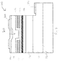
- FIG. 1a shows the lateral index step as a function of the thickness of first upper cladding layer 5 for two cladding layer laser diode structure 11 shown in FIG. lb which is similar to that of Tanaka et al.
- Tanaka et al. disclose a first upper cladding layer with a thickness of at least 100 nm which limits the lateral index, ?n, to no greater than 4 x 10 -3 .
- FIG. lb shows active region 4 beneath first upper cladding layer 5 which supports current blocking layer 6 covered by second upper cladding layer 7.
- Curve 50 shows that as the thickness of first upper cladding layer 5 increases for two cladding layer structure 11, the lateral index step (and the resulting optical confinement) drops from an initial lateral index step of about 11 x 10 -3 at zero thickness.
- an inner-stripe nitride laser diode structure (100) comprising:
- an inner-stripe nitride laser diode structure (100) comprising:
- an inner-stripe nitride laser diode structure comprising:
- the structure of an inner stripe laser may be modified to produce lateral index guiding and provide the beam quality necessary for printing and optical storage.
- the modified inner stripe laser structure allows for excellent beam quality and modal discrimination while retaining the benefits of the basic inner stripe laser structure.
- the modified inner stripe structure is applicable to nitride laser diode structures and other material systems which are relatively insensitive to regrowth interfaces close to the active region. In AlGaAs and AlGaInP laser systems, for example, the defect states associated with a regrowth interface close to the active region are sufficient to inhibit lasing.
- the modified inner stripe laser structure involves an epitaxial growth of a conventional inner stripe laser structure including a partial upper waveguide layer. A current blocking layer is then grown on the partial upper waveguide layer with a narrow stripe subsequently opened in the blocking layer. Following definition of the narrow stripe, an epitaxial regrowth is performed to complete the upper waveguide layer along with the cladding and contact layers. Finally, the structure is processed in the standard manner, including contact metallization and mirror formation.
- a positive lateral index guide may be created.
- the thickness of the waveguide in the narrow stripe region is made greater than the thickness of the wing regions of the waveguide.
- the wing regions of the upper waveguide are the waveguide regions beneath the blocking layer next to the active region. The difference in thickness functions to produce a lateral index step.
- the strength of the lateral index waveguiding depends in part on how close the blocking layer is placed to the active region with closer placement providing better lateral index guiding.
- the current blocking layer may be n-type or insulating material and materials that may be used for the current blocking layer include AlGaN, AlN, SiO 2 , SiON and Si 3 N 4 .
- Typical values of the lateral index step obtained in accordance with the invention are about 20 x 10 -3 .
- An index-guided inner stripe laser diode structure is realizable if the regrowth interface can be placed close to the active region which is possible if the regrowth interface is relatively benign.
- the regrowth interface is often structurally defective or chemically contaminated.
- material systems such as nitrides that may be used for laser diodes are relatively insensitive to regrowth interfaces near the active region and this insensitivity allows epitaxial regrowth to be performed within a waveguide of the laser diode structure.
- Regrowth allows the incorporation of a current blocking layer which has a low refractive index (typically less than n ⁇ 2.5) to enhance optical confinement.
- the current blocking layer material is selected to be thermally stable to avoid decomposition in a metalorganic chemical vapor deposition (MOCVD) environment which typically has temperatures in excess of 900 °C and a reactive ambient.
- MOCVD metalorganic chemical vapor deposition
- the current blocking layer may be insulating or semiconductor material, in the latter case a current blocking reverse bias junction is created to confine current flow to the active region by doping the current blocking layer.
- Semiconductor current blocking layers have a relatively high refractive index which limits the index step available for optical confinement. Advantages of semiconductor current blocking layers include thermal stability and straightforward regrowth. Conformal growth results in uniform surface coating whereas selective growth results in crystal nucleation only in select areas.
- Regrowth of semiconductor material performed at a temperature of about 900 °C is conformal; but for GaN growth no deposition occurs on Si 3 N 4 , SiO 2 or similar insulating material, i.e., the growth is selective. However, for AlGaN growth, polycrystalline material with rough surfaces is deposited on Si 3 N 4 , SiO 2 or similar insulating material.
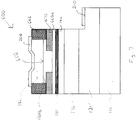
- FIGs. 2- 5 show the fabrication procedure for index-guided inner stripe nitride laser structure 100 in accordance with an embodiment of the invention.
- Standard epitaxial growth for nitride materials see, for example, U.S. Pat. Application, Ser. No. 09/288,879, by Van de Walle et al.
- CAIBE chemically assisted ion beam etching
- etching typically involves using an argon ion beam and a Cl 2 /BCl 3 gas mixture to supply the reactive gas species.
- Typical widths for stripe window 250 are from about 1-5 ⁇ m. Photoresist is stripped and acid cleaning is performed on partial laser diode structure 100 as shown in FIG. 3 prior to resumption of MOCVD growth.
- FIG. 4a shows epitaxial regrowth of upper portion 160b of GaN:Mg waveguide layer 160, AlGaN:Mg p-cladding layer 180 (typically 0.5 - 1 ⁇ m thickness) and GaN:Mg p-contact layer 190 (typically about 0.1 ⁇ m thickness). Note that the regrowth resumes with the addition of upper portion 160b of GaN:Mg waveguide instead of proceeding directly to growth of AlGaN:Mg p-cladding layer 180 so that the thickness of GaN:Mg waveguide 160 in stripe region 250 is thicker than layer 160a.
- Epitaxial overgrowth of AlGaN blocking layer 170 may be made difficult by blocking layer 170's native oxide. Overgrowth may be facilitated by capping AlGaN current blocking layer 170 with a thin n-GaN layer (not shown) or by grading the aluminum content of AlGaN blocking layer 170 down to GaN or a lower aluminum content alloy.
- AlGaN current blocking layer 170 presents a tradeoff associated with the aluminum content.
- a high aluminum composition (typically above 20%) is desirable for optimal lateral index guiding but high aluminum alloys are more prone to cracking as AlGaN current blocking layer 170 is thickened.
- AlGaN current blocking layer 170 is chosen to be thinner as the aluminum content is increased.
- the layer thickness needs to be reduced by about a factor of two to prevent cracking of the layer.
- AlGaN current blocking layer 170 may be replaced by AlGaN/GaN short period superlattice layer 175 shown in FIG. 4b having a period between 5 ⁇ to 1000 ⁇ , with a typical superlattice period of 50 ⁇ (25 ⁇ AlGaN/25 ⁇ GaN). Growth conditions are similar to those for bulk AlGaN:Si layers.
- Aluminum content in AlGaN/GaN short period superlattice layer 175 may be varied in the range between 0 percent to 100 percent with a typical range between 40 percent to 100 percent with the average aluminum content in AlGaN/GaN short period superlattice 175 typically ranging from 20 - 50 percent.
- AlGaN/GaN short period superlattice allows increased current blocking layer thickness or increased average aluminum content, typically a factor of two, before onset of layer cracking.
- AlGaN/GaN short period superlattice layer 175 is typically doped with silicon throughout layer 175. Alternatively, AlGaN/GaN short period superlattice layer 175 may be doped only in GaN layers 182, 184, 186 ... 188 or AlGaN layers 181, 183, 185 ...187 or not doped.
- short period superlattice 175 is typically capped with AlGaN:Si layer 181.
- the thickness of short period superlattice 175 can be non-destructively and very accurately measured by x-ray diffraction. Precise knowledge of current blocking layer 175 is important for the chemically assisted ion beam etch (CAIBE) step defining window 250 in current blocking layer 175 to avoid etching through GaN:Mg layer 160a into multiple quantum well region 150.
- CAIBE chemically assisted ion beam etch
- AIN is chosen for current blocking layer 170
- deposition of an amorphous or polycrystalline film by sputtering may be preferable to epitaxial growth. This retains a low refractive index for current blocking layer 170 while avoiding lattice strain that leads to cracking. Care should be taken to avoid poor structural quality that contributes to large scattering and absorption losses.
- FIG. 5 shows metallization for p-contact 200 and n-contact 210.
- Palladium p-metal for p-contact 200 is alloyed at about 535°C for about 5 minutes in an N 2 ambient.
- the first mirror is photolithographically defined and etched using CAIBE.
- the deposited palladium p-metal layer is first chemically etched.
- CAIBE etching is performed to a depth of about 2 ⁇ m to penetrate into GaN:Si layer 120 under AlGaN:Si cladding layer 130. Hence, the CAIBE etching exposes the area for n-contact 210.
- the second mirror is similarly etched.
- Liftoff metallization typically Ti-Al
- Ti-Au metallization builds up metal thickness on p-contact 200 and n-contact 210.
- the first and second mirrors are coated with SiO 2 /TiO 2 using an evaporative process.
- FIG. 6 shows effective transverse refractive index curve and optical confinement factor with curve 520 and curve 540, respectively, as a function of the thickness, t, of GaN:Mg waveguide 160 for an embodiment of nitride laser diode structure 100 in accordance with the present invention.
- Al 0.07 Ga 0.93 N cladding layers 180 and 130 have a refractive index of 2.46 at 400 nm wavelength
- 100 nm GaN waveguide 140 has a refractive index of 2.51
- multiple quantum well active region 150 has four 35 ⁇ In 0.15 Ga 0.85 N quantum wells with a refractive index of 2.56 that are separated by 65 ⁇ In 0.03 Ga 0.97 N barriers with a refractive index of 2.52. From the calculated transverse effective indices, a lateral index profile may be obtained for index-guided inner stripe nitride laser structure 100.
- N-blocking layer 170 is formed of Al 0.07 Ga 0.93 N which is the same alloy used in cladding layers 180 and 130. Higher aluminum content blocking layers may be used to produce larger index steps if cracking or overgrowth problems are avoided or short period superlattice 175 may be used instead.
- n-blocking layer 170 is grown 50nm above multiple quantum well active region 150, 100 nm of GaN:Mg is deposited after photolithographically defining narrow stripe window stripe 250 to complete waveguide layer 160 followed by a typical Al 0.07 Ga 0.93 N cladding layer having a thickness from about 0.4-0.5 ⁇ m and GaN:Mg capping layer 190.
- complete GaN waveguide 160 is about 100 nm thicker in the stripe region of waveguide layer 160 in comparison to the thickness of partial waveguide layer 160a.
- the resulting transverse effective refractive indices are shown in table 1 below: Region GaN:Mg waveguide 160 thickness transverse effective refractive index stripe region of layer 160 150nm 2.488 partial waveguide layer 160a 50nm 2.479 ⁇ N - 0.009
- the transverse effective refractive index step, ⁇ n, of 0.009 is greater than the refractive index step achieved in a conventional nitride ridge waveguide laser structure while allowing much easier fabrication of a narrow stripe structure. Furthermore, the optical confinement factor is not compromised since waveguide 160 thickness of 150 nm in the stripe region of layer 160 produces an optical confinement factor that is very nearly maximized (see FIG. 6).
- current blocking layers may also be formed from lower refractive index insulating materials such as SiON, Si 3 N 4 , or SiO 2 to provide a larger refractive index step and greater lateral index waveguiding.
- lower refractive index insulating materials such as SiON, Si 3 N 4 , or SiO 2
- SiON silicon
- Si 3 N 4 silicon oxide
- SiO 2 with a refractive index of 1.50 for current blocking layer 670 significantly increases the lateral refractive index step in comparison to Al 0.07 Ga 0.93 N blocking layer 170 placed a comparable distance from multiple quantum well active region 150.
- Current blocking layer 670 is deposited after the first epitaxy in contrast to current blocking layer 170 in FIG. 3 which is deposited during the first epitaxy.
- Insulating current blocking layer 670 may be deposited by sputtering, evaporation or high temperature CVD process.
- Narrow stripe window 650 is photolithographically defined followed by CAIBE or plasma etching with CF 4 /O 2 into, but not through, waveguide layer 660a.
- the transverse effective refractive indices for SiO 2 blocking layer 670 are summarized in table 2 below: Region GaN:Mg waveguide 660 thickness transverse effective refractive index stripe region of layer 660 150nm 2.480 partial waveguide layer 660a 50nm 2.460 ⁇ N - 0.020
- waveguide layer 660 is epitaxially laterally grown over SiO 2 current blocking layer 670 followed by deposition of Al 0.07 Ga 0.93 N cladding layer 180.
- Inner stripe 650 is opened in current blocking layer 670 to allow for current flow to multiple quantum well active region 150.
- Waveguide layer 660 is made up of layers 660a and 660b.
- waveguide layer 660b typically only partially laterally overgrows current blocking layer 670 before the desired thickness for waveguide layer 660b is achieved resulting in part of current blocking layer 670 being uncovered prior to growth of AlGaN cladding layer 180.
- polycrystalline AlGaN regions 666 form over the exposed portion of current blocking layers 670 whereas epitaxial overgrowth occurs on waveguide layer 660b.
- SiO 2 blocking layer 670 is placed closer than 50 nm to multiple quantum well active region 150 the lateral index step would be increased.
- the value of 50 nm for the separation of blocking layer 670 from multiple quantum well active region 150 is conservatively selected and less separation is possible.
- SiO 2 may not have sufficient thermal stability to function as current blocking layer 670 if the SiO 2 is exposed to high temperature MOCVD process conditions.
- SiO 2 at high MOCVD temperatures may act as a source of oxygen or silicon donors which are n-type and this could make p-type doping difficult and result in degraded performance of the inner stripe laser diode.
- High quality (dense, perfectly stoichiometric) Si 3 N 4 may be deposited at high temperatures by CVD which indicates excellent thermal stability.
- Si 3 N 4 is an alternative dielectric material for current blocking layer 670 even though its refractive index is higher producing a smaller transverse refractive index step, ?n.
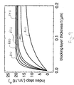
- FIG. 9 shows simulated lateral index step, ?n, as a function of current blocking layer 170 or 670 thickness assuming current blocking layer 170 or 670 is positioned 50 nm from multiple quantum well region 150.
- Curve 810 shows lateral index step ?n as a function of SiO 2 current blocking layer 670 thickness assuming a typical SiO 2 refractive index of 1.5.
- Curve 820 shows lateral index step ?n as a function of SiON current blocking layer 670 thickness assuming a typical SiON refractive index of 1.8.
- Curve 830 shows lateral index step ?n as a function of Si 3 N 4 current blocking layer 670 thickness assuming a typical Si 3 N 4 refractive index of 2.0.
- Curve 840 shows lateral index step ?n as a function of AIN current blocking layer 170 thickness assuming a typical AIN refractive index of 2.1.
- Curve 850 shows lateral index step ?n as a function of Al 0.5 Ga 0.5 N current blocking layer 170 thickness assuming a typical Al Ga 0.5 N 0.5 refractive index of 2.3.
- Curve 860 shows lateral index step ?n as a function of Al 0.2 Ga 0.8 N current blocking layer 170 thickness assuming a typical Al 0.2 Ga 0.8 N refractive index of 2.4.
- the index step for curves 810-840 plateaus for blocking layer thicknesses below about 0.08 ⁇ m while the index step for curve 850 requires a thickness of about 0.1 ⁇ m before achieving a plateau and the index step for curve 860 increases with increasing thickness beyond a 0.1 ⁇ m thickness.
- FIG. 10 shows the layer thickness required for current blocking layer 170 or 670 of a given refractive index to obtain lateral index step 910 of 5 x 10 -3 , lateral index step 920 of 10 x 10 -3 , lateral index step 930 of 15 x 10 -3 and lateral index step 940 of 20 x 10 -3 . If short period superlattice structure 175 is used for current blocking, the thickness will be the same as for current blocking layer 170 for the same aluminum content.
- the refractive indices of several representative materials SiO 2 , SiON, Si 3 N 4 , AlN, Al 0.5 Ga 0.5 N and Al 0.2 Ga 0.8 N) are denoted on the horizontal axis. It is apparent from FIG.
- the thickness of blocking layer 170 or 670 must be increased to maintain the same lateral index step.
- the thickness of blocking layer 170 or 670 is required to be thicker than 100 nm for representative materials other than SiO 2 .
- FIG. 11 shows the lateral confinement factor in percent, G lateral , versus the lateral index step for a 2 ⁇ m wide stripe laser plotted as curve 1010 and a 1 ⁇ m wide stripe laser plotted as curve 1020.
- FIG. 11 shows that improvement of the lateral confinement factor, G lateral , is marginal for a 2 ⁇ m wide stripe laser with a lateral index step greater than about 10 x 10 -3 and for a 1 ⁇ m wide stripe laser with a lateral index step greater than about 20 x 10 -3 .
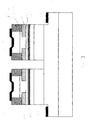
- FIG. 12 shows dual spot, inner-stripe nitride laser diode structure 1100 using semiconductor current blocking layers 170. Quadspot lasers or other multispot configurations are also realizable using the inner-stripe structure disclosed.
- the two lasers making up dual spot, inner-stripe laser diode 1110 individually have essentially the same layer structure as laser 100 shown in FIG. 5.
- Semiconductor growth over AlGaN current blocking layers 170 is epitaxial and conformal.
- FIG. 13 shows dual spot, inner-stripe nitride laser diode structure 1200 using current blocking layer 1670 made of insulating material such as, for example, SiO 2 , SiON or Si 3 N 4 .
- Current blocking layers 1670 have partial lateral overgrowth by waveguide layer 1660b that occurs during regrowth.
- waveguide layer 1660b typically only partially laterally overgrows current blocking layer 1670 before the desired thickness for layer 1660b is achieved resulting in part of current blocking layer 1670 being uncovered prior to growth of AlGaN cladding layer 1180.
- polycrystalline AlGaN regions 1666 form over the exposed portion of current blocking layers 1670 whereas epitaxial overgrowth occurs on waveguide layer 1660b. Note that overgrowth in the vicinity of the stripe is epitaxial.
- Air having a refractive index of about 1 is an alternative material for current blocking layers 670 and 1670.
- FIG. 14 shows dual spot, inner-stripe nitride laser diode structure 1200 in accordance with the invention having air as the current blocking material. SiO 2 , SiON or other selectively etchable material is used for current blocking layers 670 and 1670.
- the respective structure is treated with hydrofluoric acid, for example, to etch away the selectively etchable material by undercutting from the exposed sidewalls and leaving air gaps in to function as current blocking layer 670 or 1670.
Landscapes
- Physics & Mathematics (AREA)
- Optics & Photonics (AREA)
- Engineering & Computer Science (AREA)
- Electromagnetism (AREA)
- General Physics & Mathematics (AREA)
- Chemical & Material Sciences (AREA)
- Condensed Matter Physics & Semiconductors (AREA)
- Nanotechnology (AREA)
- Geometry (AREA)
- Life Sciences & Earth Sciences (AREA)
- Biophysics (AREA)
- Crystallography & Structural Chemistry (AREA)
- Semiconductor Lasers (AREA)
Applications Claiming Priority (2)
| Application Number | Priority Date | Filing Date | Title |
|---|---|---|---|
| US09/443,172 US6597717B1 (en) | 1999-11-19 | 1999-11-19 | Structure and method for index-guided, inner stripe laser diode structure |
| US443172 | 1999-11-19 |
Publications (3)
| Publication Number | Publication Date |
|---|---|
| EP1104059A2 true EP1104059A2 (de) | 2001-05-30 |
| EP1104059A3 EP1104059A3 (de) | 2002-09-11 |
| EP1104059B1 EP1104059B1 (de) | 2005-09-21 |
Family
ID=23759697
Family Applications (1)
| Application Number | Title | Priority Date | Filing Date |
|---|---|---|---|
| EP00309746A Expired - Lifetime EP1104059B1 (de) | 1999-11-19 | 2000-11-03 | Struktur und Verfahren für indexgeführten internen Streifendiodenlaser |
Country Status (4)
| Country | Link |
|---|---|
| US (1) | US6597717B1 (de) |
| EP (1) | EP1104059B1 (de) |
| JP (1) | JP4958334B2 (de) |
| DE (1) | DE60022723T2 (de) |
Cited By (2)
| Publication number | Priority date | Publication date | Assignee | Title |
|---|---|---|---|---|
| EP1249904A3 (de) * | 2001-04-12 | 2004-12-29 | Pioneer Corporation | Gruppe III Nitrid Verbindungen Halbleiterlaser und Herstellungsverfahren |
| CN100364192C (zh) * | 2003-04-28 | 2008-01-23 | 松下电器产业株式会社 | 半导体发光元件及其制造方法 |
Families Citing this family (16)
| Publication number | Priority date | Publication date | Assignee | Title |
|---|---|---|---|---|
| CN1259760C (zh) * | 2001-08-31 | 2006-06-14 | 三井化学株式会社 | 半导体激光元件 |
| JP3785970B2 (ja) * | 2001-09-03 | 2006-06-14 | 日本電気株式会社 | Iii族窒化物半導体素子の製造方法 |
| JP4534444B2 (ja) * | 2003-07-10 | 2010-09-01 | 日亜化学工業株式会社 | 窒化物半導体レーザ及びその製造方法 |
| JP4534435B2 (ja) * | 2003-06-27 | 2010-09-01 | 日亜化学工業株式会社 | 窒化物半導体レーザ素子及びその製造方法 |
| KR100649496B1 (ko) * | 2004-09-14 | 2006-11-24 | 삼성전기주식회사 | 질화물 반도체 발광소자 및 제조방법 |
| US20070196938A1 (en) * | 2006-02-20 | 2007-08-23 | Masahiro Ogawa | Nitride semiconductor device and method for fabricating the same |
| JP4362125B2 (ja) * | 2006-03-15 | 2009-11-11 | ローム株式会社 | 側面発光半導体素子及び側面発光半導体素子の製造方法 |
| US20080002929A1 (en) | 2006-06-30 | 2008-01-03 | Bowers John E | Electrically pumped semiconductor evanescent laser |
| JP2008187034A (ja) * | 2007-01-30 | 2008-08-14 | Sharp Corp | Iii−v族窒化物半導体レーザ素子 |
| US8111729B2 (en) * | 2008-03-25 | 2012-02-07 | Intel Corporation | Multi-wavelength hybrid silicon laser array |
| KR100969146B1 (ko) * | 2009-02-18 | 2010-07-08 | 엘지이노텍 주식회사 | 반도체 발광소자 및 그 제조방법 |
| US8890113B2 (en) * | 2011-06-08 | 2014-11-18 | Nikolay Ledentsov | Optoelectronic device with a wide bandgap and method of making same |
| DE102011083581A1 (de) * | 2011-09-28 | 2013-03-28 | Humboldt-Universität Zu Berlin | Verfahren zum herstellen eines lasers |
| DE102018123019A1 (de) * | 2018-09-19 | 2020-03-19 | Osram Opto Semiconductors Gmbh | Gewinngeführter halbleiterlaser und herstellungsverfahren hierfür |
| JP7616600B2 (ja) * | 2021-03-04 | 2025-01-17 | 豊田合成株式会社 | 半導体発光素子 |
| JP2024019871A (ja) * | 2022-08-01 | 2024-02-14 | 住友電気工業株式会社 | 半導体レーザ素子およびその製造方法 |
Family Cites Families (13)
| Publication number | Priority date | Publication date | Assignee | Title |
|---|---|---|---|---|
| JPS60116188A (ja) | 1983-11-28 | 1985-06-22 | Sharp Corp | 半導体レ−ザ素子 |
| JP3432909B2 (ja) * | 1994-09-28 | 2003-08-04 | ローム株式会社 | 半導体レーザ |
| JPH0897507A (ja) * | 1994-09-29 | 1996-04-12 | Rohm Co Ltd | 半導体レーザ |
| DE69517044T2 (de) * | 1994-10-18 | 2000-10-26 | Mitsui Chemicals, Inc. | Halbleiterlaservorrichtung |
| JPH09270569A (ja) * | 1996-01-25 | 1997-10-14 | Matsushita Electric Ind Co Ltd | 半導体レーザ装置 |
| JPH1027947A (ja) * | 1996-07-12 | 1998-01-27 | Matsushita Electric Ind Co Ltd | 半導体レーザ |
| JPH1093192A (ja) * | 1996-07-26 | 1998-04-10 | Toshiba Corp | 窒化ガリウム系化合物半導体レーザ及びその製造方法 |
| US5812576A (en) * | 1996-08-26 | 1998-09-22 | Xerox Corporation | Loss-guided semiconductor lasers |
| JP3593441B2 (ja) * | 1996-09-26 | 2004-11-24 | 株式会社東芝 | 窒化物系化合物半導体発光素子およびその製造方法 |
| JPH10126010A (ja) * | 1996-10-23 | 1998-05-15 | Ricoh Co Ltd | 半導体レーザ装置の製造方法 |
| JPH11154775A (ja) * | 1997-09-18 | 1999-06-08 | Mitsui Chem Inc | 半導体レーザの製造方法 |
| JPH11284282A (ja) | 1998-03-31 | 1999-10-15 | Fuji Photo Film Co Ltd | 短波長発光素子 |
| JP2000058969A (ja) | 1998-08-04 | 2000-02-25 | Mitsui Chemicals Inc | 半導体レーザ装置 |
-
1999
- 1999-11-19 US US09/443,172 patent/US6597717B1/en not_active Expired - Lifetime
-
2000
- 2000-11-03 EP EP00309746A patent/EP1104059B1/de not_active Expired - Lifetime
- 2000-11-03 DE DE60022723T patent/DE60022723T2/de not_active Expired - Lifetime
- 2000-11-10 JP JP2000342899A patent/JP4958334B2/ja not_active Expired - Lifetime
Cited By (2)
| Publication number | Priority date | Publication date | Assignee | Title |
|---|---|---|---|---|
| EP1249904A3 (de) * | 2001-04-12 | 2004-12-29 | Pioneer Corporation | Gruppe III Nitrid Verbindungen Halbleiterlaser und Herstellungsverfahren |
| CN100364192C (zh) * | 2003-04-28 | 2008-01-23 | 松下电器产业株式会社 | 半导体发光元件及其制造方法 |
Also Published As
| Publication number | Publication date |
|---|---|
| EP1104059B1 (de) | 2005-09-21 |
| JP4958334B2 (ja) | 2012-06-20 |
| JP2001156404A (ja) | 2001-06-08 |
| EP1104059A3 (de) | 2002-09-11 |
| DE60022723T2 (de) | 2006-04-27 |
| US6597717B1 (en) | 2003-07-22 |
| DE60022723D1 (de) | 2005-10-27 |
Similar Documents
| Publication | Publication Date | Title |
|---|---|---|
| US7042011B2 (en) | Compound semiconductor laser | |
| US6597717B1 (en) | Structure and method for index-guided, inner stripe laser diode structure | |
| US7700963B2 (en) | Nitride semiconductor light-emitting device | |
| EP1406360B1 (de) | Halbleiterlaserelement | |
| US20090010292A1 (en) | Nitride-based semiconductor laser device | |
| US7369593B2 (en) | Semiconductor laser and method for manufacturing the same | |
| US5336635A (en) | Manufacturing method of semiconductor laser of patterned-substrate type | |
| JPH07162095A (ja) | 半導体レーザ | |
| JP2001111171A (ja) | 自己整合インデックスガイド型埋め込みヘテロ構造窒化物レーザ構造 | |
| EP1104947A2 (de) | Nitrid-Halbleiterlaser und Herstellungsverfahren für denselben | |
| JP2008028375A (ja) | 窒化物半導体レーザ素子 | |
| JP4045792B2 (ja) | 窒化物半導体レーザ素子 | |
| JPH09307193A (ja) | 窒化物半導体レーザ素子及びその製造方法 | |
| JP4497606B2 (ja) | 半導体レーザ装置 | |
| US6563140B1 (en) | Semiconductor light emitting device and method for producing the same | |
| JP2006140387A (ja) | 窒化物半導体レ−ザ及びその製造方法 | |
| JP2008181928A (ja) | 半導体レーザおよびその製造方法 | |
| JP2940106B2 (ja) | 半導体レーザの製法 | |
| JP3005998B2 (ja) | 半導体レーザの製造方法 | |
| JPH07147459A (ja) | AlGaInP系半導体レーザとその製法 |
Legal Events
| Date | Code | Title | Description |
|---|---|---|---|
| PUAI | Public reference made under article 153(3) epc to a published international application that has entered the european phase |
Free format text: ORIGINAL CODE: 0009012 |
|
| AK | Designated contracting states |
Kind code of ref document: A2 Designated state(s): AT BE CH CY DE DK ES FI FR GB GR IE IT LI LU MC NL PT SE TR |
|
| AX | Request for extension of the european patent |
Free format text: AL;LT;LV;MK;RO;SI |
|
| PUAL | Search report despatched |
Free format text: ORIGINAL CODE: 0009013 |
|
| AK | Designated contracting states |
Kind code of ref document: A3 Designated state(s): AT BE CH CY DE DK ES FI FR GB GR IE IT LI LU MC NL PT SE TR |
|
| AX | Request for extension of the european patent |
Free format text: AL;LT;LV;MK;RO;SI |
|
| 17P | Request for examination filed |
Effective date: 20030311 |
|
| AKX | Designation fees paid |
Designated state(s): DE FR GB |
|
| 17Q | First examination report despatched |
Effective date: 20030430 |
|
| GRAP | Despatch of communication of intention to grant a patent |
Free format text: ORIGINAL CODE: EPIDOSNIGR1 |
|
| GRAS | Grant fee paid |
Free format text: ORIGINAL CODE: EPIDOSNIGR3 |
|
| GRAA | (expected) grant |
Free format text: ORIGINAL CODE: 0009210 |
|
| AK | Designated contracting states |
Kind code of ref document: B1 Designated state(s): DE FR GB |
|
| REG | Reference to a national code |
Ref country code: GB Ref legal event code: FG4D |
|
| REF | Corresponds to: |
Ref document number: 60022723 Country of ref document: DE Date of ref document: 20051027 Kind code of ref document: P |
|
| ET | Fr: translation filed | ||
| PLBE | No opposition filed within time limit |
Free format text: ORIGINAL CODE: 0009261 |
|
| STAA | Information on the status of an ep patent application or granted ep patent |
Free format text: STATUS: NO OPPOSITION FILED WITHIN TIME LIMIT |
|
| 26N | No opposition filed |
Effective date: 20060622 |
|
| REG | Reference to a national code |
Ref country code: FR Ref legal event code: PLFP Year of fee payment: 16 |
|
| REG | Reference to a national code |
Ref country code: FR Ref legal event code: PLFP Year of fee payment: 17 |
|
| REG | Reference to a national code |
Ref country code: FR Ref legal event code: PLFP Year of fee payment: 18 |
|
| REG | Reference to a national code |
Ref country code: FR Ref legal event code: PLFP Year of fee payment: 19 |
|
| PGFP | Annual fee paid to national office [announced via postgrant information from national office to epo] |
Ref country code: DE Payment date: 20181023 Year of fee payment: 19 |
|
| PGFP | Annual fee paid to national office [announced via postgrant information from national office to epo] |
Ref country code: FR Payment date: 20181024 Year of fee payment: 19 Ref country code: GB Payment date: 20181024 Year of fee payment: 19 |
|
| REG | Reference to a national code |
Ref country code: DE Ref legal event code: R119 Ref document number: 60022723 Country of ref document: DE |
|
| GBPC | Gb: european patent ceased through non-payment of renewal fee |
Effective date: 20191103 |
|
| PG25 | Lapsed in a contracting state [announced via postgrant information from national office to epo] |
Ref country code: GB Free format text: LAPSE BECAUSE OF NON-PAYMENT OF DUE FEES Effective date: 20191103 Ref country code: FR Free format text: LAPSE BECAUSE OF NON-PAYMENT OF DUE FEES Effective date: 20191130 Ref country code: DE Free format text: LAPSE BECAUSE OF NON-PAYMENT OF DUE FEES Effective date: 20200603 |