EP1107302A2 - Apparat und Methode, fixierte Ladungen in einem Halbleiter zu reduzieren - Google Patents
Apparat und Methode, fixierte Ladungen in einem Halbleiter zu reduzieren Download PDFInfo
- Publication number
- EP1107302A2 EP1107302A2 EP00126846A EP00126846A EP1107302A2 EP 1107302 A2 EP1107302 A2 EP 1107302A2 EP 00126846 A EP00126846 A EP 00126846A EP 00126846 A EP00126846 A EP 00126846A EP 1107302 A2 EP1107302 A2 EP 1107302A2
- Authority
- EP
- European Patent Office
- Prior art keywords
- layer
- transition
- transition layer
- deposition
- gas
- Prior art date
- Legal status (The legal status is an assumption and is not a legal conclusion. Google has not performed a legal analysis and makes no representation as to the accuracy of the status listed.)
- Withdrawn
Links
Images


Classifications
-
- H—ELECTRICITY
- H10—SEMICONDUCTOR DEVICES; ELECTRIC SOLID-STATE DEVICES NOT OTHERWISE PROVIDED FOR
- H10P—GENERIC PROCESSES OR APPARATUS FOR THE MANUFACTURE OR TREATMENT OF DEVICES COVERED BY CLASS H10
- H10P14/00—Formation of materials, e.g. in the shape of layers or pillars
- H10P14/20—Formation of materials, e.g. in the shape of layers or pillars of semiconductor materials
-
- C—CHEMISTRY; METALLURGY
- C23—COATING METALLIC MATERIAL; COATING MATERIAL WITH METALLIC MATERIAL; CHEMICAL SURFACE TREATMENT; DIFFUSION TREATMENT OF METALLIC MATERIAL; COATING BY VACUUM EVAPORATION, BY SPUTTERING, BY ION IMPLANTATION OR BY CHEMICAL VAPOUR DEPOSITION, IN GENERAL; INHIBITING CORROSION OF METALLIC MATERIAL OR INCRUSTATION IN GENERAL
- C23C—COATING METALLIC MATERIAL; COATING MATERIAL WITH METALLIC MATERIAL; SURFACE TREATMENT OF METALLIC MATERIAL BY DIFFUSION INTO THE SURFACE, BY CHEMICAL CONVERSION OR SUBSTITUTION; COATING BY VACUUM EVAPORATION, BY SPUTTERING, BY ION IMPLANTATION OR BY CHEMICAL VAPOUR DEPOSITION, IN GENERAL
- C23C16/00—Chemical coating by decomposition of gaseous compounds, without leaving reaction products of surface material in the coating, i.e. chemical vapour deposition [CVD] processes
- C23C16/44—Chemical coating by decomposition of gaseous compounds, without leaving reaction products of surface material in the coating, i.e. chemical vapour deposition [CVD] processes characterised by the method of coating
- C23C16/455—Chemical coating by decomposition of gaseous compounds, without leaving reaction products of surface material in the coating, i.e. chemical vapour deposition [CVD] processes characterised by the method of coating characterised by the method used for introducing gases into reaction chamber or for modifying gas flows in reaction chamber
- C23C16/45523—Pulsed gas flow or change of composition over time
-
- C—CHEMISTRY; METALLURGY
- C23—COATING METALLIC MATERIAL; COATING MATERIAL WITH METALLIC MATERIAL; CHEMICAL SURFACE TREATMENT; DIFFUSION TREATMENT OF METALLIC MATERIAL; COATING BY VACUUM EVAPORATION, BY SPUTTERING, BY ION IMPLANTATION OR BY CHEMICAL VAPOUR DEPOSITION, IN GENERAL; INHIBITING CORROSION OF METALLIC MATERIAL OR INCRUSTATION IN GENERAL
- C23C—COATING METALLIC MATERIAL; COATING MATERIAL WITH METALLIC MATERIAL; SURFACE TREATMENT OF METALLIC MATERIAL BY DIFFUSION INTO THE SURFACE, BY CHEMICAL CONVERSION OR SUBSTITUTION; COATING BY VACUUM EVAPORATION, BY SPUTTERING, BY ION IMPLANTATION OR BY CHEMICAL VAPOUR DEPOSITION, IN GENERAL
- C23C16/00—Chemical coating by decomposition of gaseous compounds, without leaving reaction products of surface material in the coating, i.e. chemical vapour deposition [CVD] processes
- C23C16/02—Pretreatment of the material to be coated
- C23C16/0272—Deposition of sub-layers, e.g. to promote the adhesion of the main coating
- C23C16/029—Graded interfaces
-
- H—ELECTRICITY
- H10—SEMICONDUCTOR DEVICES; ELECTRIC SOLID-STATE DEVICES NOT OTHERWISE PROVIDED FOR
- H10P—GENERIC PROCESSES OR APPARATUS FOR THE MANUFACTURE OR TREATMENT OF DEVICES COVERED BY CLASS H10
- H10P14/00—Formation of materials, e.g. in the shape of layers or pillars
- H10P14/60—Formation of materials, e.g. in the shape of layers or pillars of insulating materials
- H10P14/69—Inorganic materials
- H10P14/692—Inorganic materials composed of oxides, glassy oxides or oxide-based glasses
- H10P14/6921—Inorganic materials composed of oxides, glassy oxides or oxide-based glasses containing silicon
- H10P14/6922—Inorganic materials composed of oxides, glassy oxides or oxide-based glasses containing silicon the material containing Si, O and at least one of H, N, C, F or other non-metal elements, e.g. SiOC, SiOC:H or SiONC
-
- H—ELECTRICITY
- H10—SEMICONDUCTOR DEVICES; ELECTRIC SOLID-STATE DEVICES NOT OTHERWISE PROVIDED FOR
- H10P—GENERIC PROCESSES OR APPARATUS FOR THE MANUFACTURE OR TREATMENT OF DEVICES COVERED BY CLASS H10
- H10P14/00—Formation of materials, e.g. in the shape of layers or pillars
- H10P14/60—Formation of materials, e.g. in the shape of layers or pillars of insulating materials
- H10P14/63—Formation of materials, e.g. in the shape of layers or pillars of insulating materials characterised by the formation processes
- H10P14/6326—Deposition processes
- H10P14/6328—Deposition from the gas or vapour phase
- H10P14/6334—Deposition from the gas or vapour phase using decomposition or reaction of gaseous or vapour phase compounds, i.e. chemical vapour deposition
- H10P14/6336—Deposition from the gas or vapour phase using decomposition or reaction of gaseous or vapour phase compounds, i.e. chemical vapour deposition in the presence of a plasma [PECVD]
-
- H—ELECTRICITY
- H10—SEMICONDUCTOR DEVICES; ELECTRIC SOLID-STATE DEVICES NOT OTHERWISE PROVIDED FOR
- H10P—GENERIC PROCESSES OR APPARATUS FOR THE MANUFACTURE OR TREATMENT OF DEVICES COVERED BY CLASS H10
- H10P14/00—Formation of materials, e.g. in the shape of layers or pillars
- H10P14/60—Formation of materials, e.g. in the shape of layers or pillars of insulating materials
- H10P14/66—Formation of materials, e.g. in the shape of layers or pillars of insulating materials characterised by the type of materials
- H10P14/662—Laminate layers, e.g. stacks of alternating high-k metal oxides
-
- H—ELECTRICITY
- H10—SEMICONDUCTOR DEVICES; ELECTRIC SOLID-STATE DEVICES NOT OTHERWISE PROVIDED FOR
- H10P—GENERIC PROCESSES OR APPARATUS FOR THE MANUFACTURE OR TREATMENT OF DEVICES COVERED BY CLASS H10
- H10P14/00—Formation of materials, e.g. in the shape of layers or pillars
- H10P14/60—Formation of materials, e.g. in the shape of layers or pillars of insulating materials
- H10P14/66—Formation of materials, e.g. in the shape of layers or pillars of insulating materials characterised by the type of materials
- H10P14/668—Formation of materials, e.g. in the shape of layers or pillars of insulating materials characterised by the type of materials the materials being characterised by the deposition precursor materials
- H10P14/6681—Formation of materials, e.g. in the shape of layers or pillars of insulating materials characterised by the type of materials the materials being characterised by the deposition precursor materials the precursor containing a compound comprising Si
- H10P14/6682—Formation of materials, e.g. in the shape of layers or pillars of insulating materials characterised by the type of materials the materials being characterised by the deposition precursor materials the precursor containing a compound comprising Si the compound being a silane, e.g. disilane, methylsilane or chlorosilane
-
- H—ELECTRICITY
- H10—SEMICONDUCTOR DEVICES; ELECTRIC SOLID-STATE DEVICES NOT OTHERWISE PROVIDED FOR
- H10P—GENERIC PROCESSES OR APPARATUS FOR THE MANUFACTURE OR TREATMENT OF DEVICES COVERED BY CLASS H10
- H10P14/00—Formation of materials, e.g. in the shape of layers or pillars
- H10P14/60—Formation of materials, e.g. in the shape of layers or pillars of insulating materials
- H10P14/69—Inorganic materials
- H10P14/6903—Inorganic materials containing silicon
- H10P14/6905—Inorganic materials containing silicon being a silicon carbide or silicon carbonitride and not containing oxygen, e.g. SiC or SiC:H
-
- H—ELECTRICITY
- H10—SEMICONDUCTOR DEVICES; ELECTRIC SOLID-STATE DEVICES NOT OTHERWISE PROVIDED FOR
- H10P—GENERIC PROCESSES OR APPARATUS FOR THE MANUFACTURE OR TREATMENT OF DEVICES COVERED BY CLASS H10
- H10P14/00—Formation of materials, e.g. in the shape of layers or pillars
- H10P14/60—Formation of materials, e.g. in the shape of layers or pillars of insulating materials
- H10P14/69—Inorganic materials
- H10P14/692—Inorganic materials composed of oxides, glassy oxides or oxide-based glasses
- H10P14/6921—Inorganic materials composed of oxides, glassy oxides or oxide-based glasses containing silicon
- H10P14/69215—Inorganic materials composed of oxides, glassy oxides or oxide-based glasses containing silicon the material being a silicon oxide, e.g. SiO2
-
- Y—GENERAL TAGGING OF NEW TECHNOLOGICAL DEVELOPMENTS; GENERAL TAGGING OF CROSS-SECTIONAL TECHNOLOGIES SPANNING OVER SEVERAL SECTIONS OF THE IPC; TECHNICAL SUBJECTS COVERED BY FORMER USPC CROSS-REFERENCE ART COLLECTIONS [XRACs] AND DIGESTS
- Y10—TECHNICAL SUBJECTS COVERED BY FORMER USPC
- Y10S—TECHNICAL SUBJECTS COVERED BY FORMER USPC CROSS-REFERENCE ART COLLECTIONS [XRACs] AND DIGESTS
- Y10S438/00—Semiconductor device manufacturing: process
- Y10S438/931—Silicon carbide semiconductor
-
- Y—GENERAL TAGGING OF NEW TECHNOLOGICAL DEVELOPMENTS; GENERAL TAGGING OF CROSS-SECTIONAL TECHNOLOGIES SPANNING OVER SEVERAL SECTIONS OF THE IPC; TECHNICAL SUBJECTS COVERED BY FORMER USPC CROSS-REFERENCE ART COLLECTIONS [XRACs] AND DIGESTS
- Y10—TECHNICAL SUBJECTS COVERED BY FORMER USPC
- Y10S—TECHNICAL SUBJECTS COVERED BY FORMER USPC CROSS-REFERENCE ART COLLECTIONS [XRACs] AND DIGESTS
- Y10S438/00—Semiconductor device manufacturing: process
- Y10S438/94—Laser ablative material removal
-
- Y—GENERAL TAGGING OF NEW TECHNOLOGICAL DEVELOPMENTS; GENERAL TAGGING OF CROSS-SECTIONAL TECHNOLOGIES SPANNING OVER SEVERAL SECTIONS OF THE IPC; TECHNICAL SUBJECTS COVERED BY FORMER USPC CROSS-REFERENCE ART COLLECTIONS [XRACs] AND DIGESTS
- Y10—TECHNICAL SUBJECTS COVERED BY FORMER USPC
- Y10S—TECHNICAL SUBJECTS COVERED BY FORMER USPC CROSS-REFERENCE ART COLLECTIONS [XRACs] AND DIGESTS
- Y10S438/00—Semiconductor device manufacturing: process
- Y10S438/942—Masking
- Y10S438/948—Radiation resist
- Y10S438/952—Utilizing antireflective layer
Definitions
- the invention relates to the fabrication of semiconductor devices and, more particularly, the invention relates to a method and apparatus for reducing the amount of charges that are trapped between layers of a semiconductor device during its fabrication.
- Integrated circuits fabricated on semiconductor substrates for Ultra Large Scale Integration require multiple levels of interconnections for electrically connecting the discrete semiconductor devices that comprise the circuits.
- the multiple levels of interconnections are separated by layers of insulating material. These interposed insulating layers have etched via holes which are used to connect one level of interconnections to another.
- the insulating layer material is silicon oxide (SiO 2 ) having a dielectric constant (relative to vacuum) of about 4.1 to 4.5.
- the intra- (on the same metal level) and interlevel (between metal levels) capacitances increase when insulating layers therebetween have the same dielectric constant.
- the signal propagation time in the circuit is adversely affected by the RC delay time, where R is the resistance of the metal line, and C is the inter- and/or the intralevel capacitance mentioned above.
- FIG. 1 depicts an integrated circuit device 100 that is presently known in the art.
- the device 100 is comprised of a substrate material 102 (typically a dielectric material such as SiO 2 ) having a plurality of layers 103 of various materials disposed thereupon.
- the various layers have different electrical properties so as to create conductive pathways, circuit devices, and the like.
- a first layer 104 is an insulating layer disposed on top of the substrate 102 acting as a primary insulator.
- various circuit pathways or circuit devices 106 comprised of conductive material such as titanium or aluminum.
- a second insulative layer 108 Disposed above the insulating and conductive layers, 104 and 106 respectively, is a second insulative layer 108.
- the second insulative layer 108 is a dielectric material but not necessarily the same material as the first dielectric layer 104.
- One approach to minimize the RC time delays is to use a good electrical conductor for the interconnection levels, such as replacing the titanium or aluminum with copper to reduce resistance R.
- a second approach is to use an insulating material that has a lower dielectric constant k, such as an organic, to reduce the capacitance C between the interconnection levels.
- k such as an organic
- a typical low k dielectric material that is currently in use for the fabrication of integrated circuits is the compound trimethylsilane (3MS).
- the dielectric constant of this material is approximately 2.7; therefore, is highly preferred for use as a dielectric material between conductive areas such as conductive pathways and devices and the like represented as 106.
- a well known method for creating integrated circuits such as those described above is by chemical vapor deposition (CVD).
- CVD chemical vapor deposition
- a precursor gas is mixed with a carrier gas and introduced to a deposition chamber at an elevated temperature.
- the precursor gas Upon contact with a substrate 102 within the chamber, the precursor gas decomposes into various elements and reacts with the surface to create the desired material (insulative layer 104, typically an oxide or conductive material 106, i.e., copper.
- Such processes may also be enhanced by the use of a plasma within the chamber which provides for a more uniform deposition process, i.e., when filling an opening in an oxide layer 104 with conductor material 106.
- the second insulative layer 108 is also formed by CVD or plasma enhanced CVD; however, deficiencies in the process create undesirable results. For example when depositing one oxide material over another, i.e., second insulative layer 108 deposited over first insulative layer 104, different crystal planar structures and dimensions within these two materials create microscopic gaps at an interface 110 of two such layers.
- FIG. 2 shows an enlarged detail area of FIG. 1 depicting trapped electrical charges 202 at the interface 110 during the CVD process. These trapped charges 202 create a substantial charge buildup condition within the interface 110 which detrimentally effects nearby devices.
- FIG. 3 depicts a graph of capacitance vs.
- gate voltage of a device i.e., the gate structure of a MOSFET transistor device
- a flat band voltage is approximately -55 V. Since the charge trapping condition is difficult to avoid, a typical and acceptable value for flat band voltage is approximately -15 V. If there are many such trapped charges 202 at the interface 110, devices constructed on the substrate are detrimentally effected resulting in poor or non-operational condition of such devices.
- the disadvantages associated with the prior art are overcome with the present invention of a method for reducing trapped charges in a semiconductor device having a first layer and a second layer, said method comprising the steps of providing said first layer, flowing a deposition, a dilution and a conversion gas upon said first layer thereby forming a transition layer, phasing out said flow of conversion gas and forming said second layer upon said transition layer.
- the deposition gas, dilution gas and conversion gas are preferably trimethylsilane, helium and N 2 O respectively. Additionally, the step of phasing out the conversion gas flow alters the characteristics of the transition layer.
- the method is formed via chemical vapor deposition or plasma enhanced chemical vapor deposition when depositing the transition layer, first and second layers.
- a method for reducing trapped charges in a semiconductor device having a first layer and a second layer comprising the steps of providing the first layer, flowing a deposition and dilution gas upon said first layer to form a transition layer thereupon, applying a plasma treatment to said transition layer, and forming said second layer upon said transition layer.
- the deposition gas and dilution gas are preferably trimethylsilane and helium respectively.
- the plasma treatment further comprises a N 2 O plasma conducted in a range of approximately 50 to 500 watts and preferably 250 watts.
- the second layer is preferably a trimethylsilane oxide layer.
- An apparatus for reducing trapped charges in a semiconductor device has a first insulating layer, a transition layer disposed upon said first layer and a second insulating layer disposed upon said transition layer.
- the transition layer improves the adhesion between said first insulating layer and said second insulating layer and said transition layer is preferably a silicon carbide based material and most preferably SiC:H.
- the second insulating layer is trimethylsilane oxide.
- FIG. 4 depicts an integrated circuit device 400 in accordance with the present invention.
- the device 400 is comprised of a substrate material 402 (i.e., a dielectric material such as SiO 2 ) having a plurality of layers 403 of various materials disposed thereupon.
- the various layers have different electrical properties so as to create conductive pathways (also known as lines), circuit devices, and the like. These pathways and devices are linked to other devices on the substrate via a variety of other lines, interconnects and devices (not shown).
- FIG. 9 depicts an exemplary deposition system 900 for performing CVD.
- a liquid precursor 918 is delivered to a deposition chamber 902 from a precursor delivery system 908 via one or more precursor material transfer lines 920. Specifically, the liquid precursor 918 is vaporized at vaporizer 906, mixed with a carrier gas 924 and delivered to a showerhead 922 in the deposition chamber 902.
- a deposition chamber that can be used is a model DzX chamber manufactured by Applied Materials, Inc. of Santa Clara, California.
- the deposition chamber 902 contains a heated susceptor 916 for retaining the substrate 402 (i.e., a semiconductor wafer) onto which it is desirable to deposit the plurality of layers 403. Material is deposited onto the substrate 402 by CVD when the vaporized precursor contacts the heated substrate 402. Such processes may also be enhanced by the use of a plasma within the chamber which provides for a more uniform deposition process.
- the plasma is formed by driving one or more of the chamber components (i.e., the susceptor 916 or showerhead 922 with a high power energy source.
- the energy source is an AC power source 928 connected to the susceptor 916.
- the chamber 902 and precursor delivery system 908 are controlled by a process control system 904.
- the process chamber 902 is defined by a set of walls 914 that are electrically and thermally isolated from the susceptor 916 and showerhead 922 by isolators 910. Thermal energy, from a heating element 926 such as a resistive coil, heats a top surface of the susceptor 916.
- Pressure control unit 930 i.e., a vacuum pump adjusts the chamber atmosphere as necessary to facilitate deposition processes.
- a first layer 404 is an insulating layer disposed on top of the substrate 402 acting as a primary insulator.
- various circuit pathways or devices 406 comprised of conductive material such as titanium, copper, tantalum or the like.
- a transition layer 407 is disposed upon the interface 410.
- the second insulative layer 408 is a dielectric material, but not necessarily the same material as the first dielectric layer 404.
- the transition layer 407 is preferably a low k dielectric material. Such material has properties that enhance the bonding of the second insulative layer 408 to the first insulative layer 404.
- One such material that can accomplish this desired effect is BLOKTM, a trademark of Applied Materials, Inc. of Santa Clara, CA.
- the subject invention also includes a method for forming a second insulative layer upon a first insulative layer.
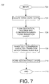
- a first embodiment of the subject method is depicted in FIG. 7 as a series of method steps 700.
- the method begins at step 702 and proceeds to step 704 wherein a first insulative layer (i.e., an oxide layer) is provided on a substrate material.
- Said first insulative layer may be for example layer 404 disposed upon a semiconductor substrate 402 for defining conductive pathways or circuit devices upon said substrate.
- a flow of deposition, dilution and conversion gases are provided to the first insulative layer. The deposition, dilution and conversion gases form a transition layer upon the first insulative layer.
- Said transition layer for example is layer 407 shown in FIG. 4.
- the flow of conversion gas is phased out (i.e., gradually turned off or diminished over time).
- the characteristics of the transition layer are altered in a gradual fashion so as to improve the likelihood of adequate bonding between the transition layer and the second insulative layer.
- a second insulative layer is formed upon the transition layer.
- the second oxide layer is, for example, layer 408 as shown in FIG. 4.
- the deposition gas is a silicon based material and in a preferred embodiment of the invention is trimethylsilane (3MS), the dilution gas is an inert gas and in a preferred embodiment is helium.
- the conversion gas is an oxygen containing gas and in a preferred embodiment of the invention is N 2 O.
- the second insulative layer is a silicon based insulating layer and in a preferred embodiment of the invention is a trimethylsilane oxide layer.
- first insulative, transition, and second insulative layers are created via methods to those skilled in the art of semiconductor circuit device fabrication and include but are not limited to physical vapor deposition (PVD), chemical vapor deposition (CVD) and the like and in a preferred embodiment of the invention the subject layers are formed via CVD, and more preferably by plasma enhanced CVD (PECVD).
- PVD physical vapor deposition
- CVD chemical vapor deposition
- PECVD plasma enhanced CVD
- the subject method can be practiced in a semiconductor fabrication chamber such as a DxZ chamber a manufactured and sold by Applied Materials, Inc. of Santa Clara, CA. The conditions under which such method takes place are as follows:
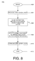
- a series of method steps 800 is used to form a second insulative layer upon a first insulative layer.
- Such method steps 800 begin at step 802 and proceed to step 804 wherein a first insulative layer is provided on a substrate.
- a flow of deposition and dilution gases is provided upon a first insulative layer to form a transition layer thereupon.
- the flow of deposition and dilution gases is halted and a plasma treatment is applied to the transition layer. The plasma treatment alters the characteristics of the transition layer so as to improve the adhesion of the second insulative layer.
- the second insulative layer is disposed upon the transition layer and the method 800 concludes at step 812.
- FIG. 5 depicts a graph of gate voltage (V) vs. capacitance (pF) for a semiconductor device formed in accordance with either of the methods disclosed.
- V gate voltage
- PPF capacitance
- FIG. 6 depicts a graph of the same characteristic for a device that has been treated under more optimized conditions (including the use of Silane) as disclosed above.
- the flatband voltage has been reduced to the typically acceptable value of -15V.
- a flatband voltage closer zero indicates that there are fewer charges trapped in the interface 410 of the subject invention than previously realized. As such, the device 400 is less susceptible to breakdown caused by generally poor or out-of-spec design.
Landscapes
- Chemical & Material Sciences (AREA)
- General Chemical & Material Sciences (AREA)
- Chemical Kinetics & Catalysis (AREA)
- Engineering & Computer Science (AREA)
- Materials Engineering (AREA)
- Mechanical Engineering (AREA)
- Metallurgy (AREA)
- Organic Chemistry (AREA)
- Formation Of Insulating Films (AREA)
- Internal Circuitry In Semiconductor Integrated Circuit Devices (AREA)
- Chemical Vapour Deposition (AREA)
Applications Claiming Priority (2)
| Application Number | Priority Date | Filing Date | Title |
|---|---|---|---|
| US457086 | 1999-12-07 | ||
| US09/457,086 US6541369B2 (en) | 1999-12-07 | 1999-12-07 | Method and apparatus for reducing fixed charges in a semiconductor device |
Publications (2)
| Publication Number | Publication Date |
|---|---|
| EP1107302A2 true EP1107302A2 (de) | 2001-06-13 |
| EP1107302A3 EP1107302A3 (de) | 2004-10-27 |
Family
ID=23815378
Family Applications (1)
| Application Number | Title | Priority Date | Filing Date |
|---|---|---|---|
| EP00126846A Withdrawn EP1107302A3 (de) | 1999-12-07 | 2000-12-07 | Apparat und Methode, fixierte Ladungen in einem Halbleiter zu reduzieren |
Country Status (6)
| Country | Link |
|---|---|
| US (1) | US6541369B2 (de) |
| EP (1) | EP1107302A3 (de) |
| JP (1) | JP4753467B2 (de) |
| KR (1) | KR20010062216A (de) |
| SG (1) | SG97169A1 (de) |
| TW (1) | TW487990B (de) |
Cited By (2)
| Publication number | Priority date | Publication date | Assignee | Title |
|---|---|---|---|---|
| WO2005033359A3 (en) * | 2003-09-23 | 2005-06-23 | Micron Technology Inc | Atomic layer deposition methods of forming silicon dioxide comprising layers |
| CN104141112B (zh) * | 2008-05-07 | 2017-09-19 | 普林斯顿大学理事会 | 用于电子器件或其他物品上的涂层中的混合层 |
Families Citing this family (6)
| Publication number | Priority date | Publication date | Assignee | Title |
|---|---|---|---|---|
| US6794295B1 (en) * | 2000-05-26 | 2004-09-21 | Taiwan Semiconductor Manufacturing Company, Ltd. | Method to improve stability and reliability of CVD low K dielectric |
| US6762132B1 (en) | 2000-08-31 | 2004-07-13 | Micron Technology, Inc. | Compositions for dissolution of low-K dielectric films, and methods of use |
| US6913992B2 (en) * | 2003-03-07 | 2005-07-05 | Applied Materials, Inc. | Method of modifying interlayer adhesion |
| US6874363B1 (en) * | 2003-10-31 | 2005-04-05 | Honeywell International, Inc. | Trapped charge field bias vibrating beam accelerometer |
| US7030041B2 (en) * | 2004-03-15 | 2006-04-18 | Applied Materials Inc. | Adhesion improvement for low k dielectrics |
| US11306395B2 (en) * | 2017-06-28 | 2022-04-19 | Asm Ip Holding B.V. | Methods for depositing a transition metal nitride film on a substrate by atomic layer deposition and related deposition apparatus |
Family Cites Families (30)
| Publication number | Priority date | Publication date | Assignee | Title |
|---|---|---|---|---|
| US4484809B1 (en) | 1977-12-05 | 1995-04-18 | Plasma Physics Corp | Glow discharge method and apparatus and photoreceptor devices made therewith |
| JPS59128281A (ja) * | 1982-12-29 | 1984-07-24 | 信越化学工業株式会社 | 炭化けい素被覆物の製造方法 |
| DE3429899A1 (de) | 1983-08-16 | 1985-03-07 | Canon K.K., Tokio/Tokyo | Verfahren zur bildung eines abscheidungsfilms |
| US4557943A (en) | 1983-10-31 | 1985-12-10 | Advanced Semiconductor Materials America, Inc. | Metal-silicide deposition using plasma-enhanced chemical vapor deposition |
| US4678679A (en) | 1984-06-25 | 1987-07-07 | Energy Conversion Devices, Inc. | Continuous deposition of activated process gases |
| JPH0692635B2 (ja) * | 1987-03-02 | 1994-11-16 | 株式会社日立製作所 | マイクロ波プラズマ薄膜形成装置 |
| JPS63280453A (ja) * | 1987-05-13 | 1988-11-17 | Nippon Telegr & Teleph Corp <Ntt> | 半導体装置およびその製造方法 |
| JPH0691082B2 (ja) * | 1988-10-13 | 1994-11-14 | 株式会社東芝 | 半導体装置の製造方法 |
| JPH02114530A (ja) | 1988-10-25 | 1990-04-26 | Mitsubishi Electric Corp | 薄膜形成装置 |
| KR100228259B1 (ko) | 1990-10-24 | 1999-11-01 | 고지마 마따오 | 박막의 형성방법 및 반도체장치 |
| JPH0548130A (ja) * | 1991-08-07 | 1993-02-26 | Canon Inc | 半導体装置とその製造方法 |
| JP2648746B2 (ja) * | 1991-09-26 | 1997-09-03 | 株式会社ジーティシー | 絶縁膜形成方法 |
| JPH06232113A (ja) * | 1993-02-02 | 1994-08-19 | Fuji Electric Co Ltd | 半導体装置用絶縁膜の堆積方法 |
| US5800686A (en) | 1993-04-05 | 1998-09-01 | Applied Materials, Inc. | Chemical vapor deposition chamber with substrate edge protection |
| AU1745695A (en) | 1994-06-03 | 1996-01-04 | Materials Research Corporation | A method of nitridization of titanium thin films |
| US5818071A (en) * | 1995-02-02 | 1998-10-06 | Dow Corning Corporation | Silicon carbide metal diffusion barrier layer |
| DE19516669A1 (de) * | 1995-05-05 | 1996-11-07 | Siemens Ag | Verfahren zur Abscheidung einer Siliziumoxidschicht |
| TW328971B (en) * | 1995-10-30 | 1998-04-01 | Dow Corning | Method for depositing Si-O containing coatings |
| US5652166A (en) | 1996-01-11 | 1997-07-29 | United Microelectronics Corporation | Process for fabricating dual-gate CMOS having in-situ nitrogen-doped polysilicon by rapid thermal chemical vapor deposition |
| US5741626A (en) * | 1996-04-15 | 1998-04-21 | Motorola, Inc. | Method for forming a dielectric tantalum nitride layer as an anti-reflective coating (ARC) |
| FR2751131B1 (fr) | 1996-07-09 | 2001-11-09 | Lg Electronics Inc | Procede de fabrication d'un dispositif d'affichage a matrice active a cristal liquide et structure du dispositif d'affichage selon ce procede |
| US6028012A (en) | 1996-12-04 | 2000-02-22 | Yale University | Process for forming a gate-quality insulating layer on a silicon carbide substrate |
| US5943599A (en) * | 1997-08-27 | 1999-08-24 | Vanguard International Semiconductor Corporation | Method of fabricating a passivation layer for integrated circuits |
| US6140226A (en) | 1998-01-16 | 2000-10-31 | International Business Machines Corporation | Dual damascene processing for semiconductor chip interconnects |
| US6287990B1 (en) | 1998-02-11 | 2001-09-11 | Applied Materials, Inc. | CVD plasma assisted low dielectric constant films |
| US6054379A (en) * | 1998-02-11 | 2000-04-25 | Applied Materials, Inc. | Method of depositing a low k dielectric with organo silane |
| US6303523B2 (en) * | 1998-02-11 | 2001-10-16 | Applied Materials, Inc. | Plasma processes for depositing low dielectric constant films |
| US6159871A (en) | 1998-05-29 | 2000-12-12 | Dow Corning Corporation | Method for producing hydrogenated silicon oxycarbide films having low dielectric constant |
| US6147009A (en) | 1998-06-29 | 2000-11-14 | International Business Machines Corporation | Hydrogenated oxidized silicon carbon material |
| JP2000223485A (ja) * | 1999-01-28 | 2000-08-11 | Nec Corp | 複合絶縁膜の製造方法及びこれを用いた半導体装置の製造方法 |
-
1999
- 1999-12-07 US US09/457,086 patent/US6541369B2/en not_active Expired - Fee Related
-
2000
- 2000-11-15 SG SG200006624A patent/SG97169A1/en unknown
- 2000-11-21 TW TW089124703A patent/TW487990B/zh not_active IP Right Cessation
- 2000-12-07 KR KR1020000074188A patent/KR20010062216A/ko not_active Withdrawn
- 2000-12-07 EP EP00126846A patent/EP1107302A3/de not_active Withdrawn
- 2000-12-07 JP JP2000372952A patent/JP4753467B2/ja not_active Expired - Fee Related
Cited By (6)
| Publication number | Priority date | Publication date | Assignee | Title |
|---|---|---|---|---|
| WO2005033359A3 (en) * | 2003-09-23 | 2005-06-23 | Micron Technology Inc | Atomic layer deposition methods of forming silicon dioxide comprising layers |
| US7018469B2 (en) | 2003-09-23 | 2006-03-28 | Micron Technology, Inc. | Atomic layer deposition methods of forming silicon dioxide comprising layers |
| KR100758758B1 (ko) * | 2003-09-23 | 2007-09-14 | 미크론 테크놀로지,인코포레이티드 | 실리콘 다이옥사이드를 포함하는 층을 형성하기 위한 원자층 증착 방법 |
| CN100577864C (zh) * | 2003-09-23 | 2010-01-06 | 美光科技公司 | 形成含二氧化硅的层的原子层沉积方法 |
| CN104141112B (zh) * | 2008-05-07 | 2017-09-19 | 普林斯顿大学理事会 | 用于电子器件或其他物品上的涂层中的混合层 |
| US9882167B2 (en) | 2008-05-07 | 2018-01-30 | The Trustees Of Princeton University | Hybrid layers for use in coatings on electronic devices or other articles |
Also Published As
| Publication number | Publication date |
|---|---|
| SG97169A1 (en) | 2003-07-18 |
| JP4753467B2 (ja) | 2011-08-24 |
| KR20010062216A (ko) | 2001-07-07 |
| US20020081759A1 (en) | 2002-06-27 |
| JP2001257206A (ja) | 2001-09-21 |
| TW487990B (en) | 2002-05-21 |
| US6541369B2 (en) | 2003-04-01 |
| EP1107302A3 (de) | 2004-10-27 |
Similar Documents
| Publication | Publication Date | Title |
|---|---|---|
| US5763010A (en) | Thermal post-deposition treatment of halogen-doped films to improve film stability and reduce halogen migration to interconnect layers | |
| US6159842A (en) | Method for fabricating a hybrid low-dielectric-constant intermetal dielectric (IMD) layer with improved reliability for multilevel interconnections | |
| US7200460B2 (en) | Method of depositing low dielectric constant silicon carbide layers | |
| US7001850B2 (en) | Method of depositing dielectric films | |
| US6582777B1 (en) | Electron beam modification of CVD deposited low dielectric constant materials | |
| US5549786A (en) | Highly selective, highly uniform plasma etch process for spin-on glass | |
| US20020048969A1 (en) | Method of forming film, method of manufacturing semiconductor device, and film forming apparatus | |
| US6951807B2 (en) | Semiconductor device and manufacturing method thereof | |
| US20020027286A1 (en) | Low leakage current silicon carbonitride prepared using methane, ammonia and silane for copper diffusion barrier, etchstop and passivation applications | |
| KR20010075566A (ko) | 반도체 장치 및 그 제조 방법 | |
| KR20110094205A (ko) | 산소 함유 전구체를 사용한 유전체 장벽 증착 | |
| JP4242648B2 (ja) | 金属イオン拡散バリア層 | |
| US6521300B1 (en) | Method of a surface treatment in improving adhesion of an organic polymeric low-k dielectric layer | |
| US6750141B2 (en) | Silicon carbide cap layers for low dielectric constant silicon oxide layers | |
| JP2004153266A (ja) | 積層構造体の形成方法及び絶縁膜の集積方法 | |
| US6541369B2 (en) | Method and apparatus for reducing fixed charges in a semiconductor device | |
| TW457558B (en) | Semiconductor device and manufacturing method thereof | |
| US20020142104A1 (en) | Plasma treatment of organosilicate layers | |
| US7381660B2 (en) | Dielectric barrier layer for a copper metallization layer having a varying silicon concentration along its thickness | |
| JP2005050954A (ja) | 半導体装置およびその製造方法 | |
| US6281584B1 (en) | Integrated circuit with improved adhesion between interfaces of conductive and dielectric surfaces | |
| US6632737B1 (en) | Method for enhancing the adhesion of a barrier layer to a dielectric | |
| KR100571643B1 (ko) | 반도체 소자의 제조방법 | |
| EP1460685A1 (de) | Halbleiterbauelement und Methode zu seiner Herstellung | |
| TW202612025A (zh) | 整合操作後之修復低k材料的方法 |
Legal Events
| Date | Code | Title | Description |
|---|---|---|---|
| PUAI | Public reference made under article 153(3) epc to a published international application that has entered the european phase |
Free format text: ORIGINAL CODE: 0009012 |
|
| AK | Designated contracting states |
Kind code of ref document: A2 Designated state(s): AT BE CH CY DE DK ES FI FR GB GR IE IT LI LU MC NL PT SE TR |
|
| AX | Request for extension of the european patent |
Free format text: AL;LT;LV;MK;RO;SI |
|
| PUAL | Search report despatched |
Free format text: ORIGINAL CODE: 0009013 |
|
| AK | Designated contracting states |
Kind code of ref document: A3 Designated state(s): AT BE CH CY DE DK ES FI FR GB GR IE IT LI LU MC NL PT SE TR |
|
| AX | Request for extension of the european patent |
Extension state: AL LT LV MK RO SI |
|
| 17P | Request for examination filed |
Effective date: 20050427 |
|
| AKX | Designation fees paid |
Designated state(s): BE CH DE GB LI NL |
|
| STAA | Information on the status of an ep patent application or granted ep patent |
Free format text: STATUS: THE APPLICATION IS DEEMED TO BE WITHDRAWN |
|
| 18D | Application deemed to be withdrawn |
Effective date: 20100113 |