EP1108468B1 - Vorrichtung zum Aufbringen von dünnen Schichten - Google Patents
Vorrichtung zum Aufbringen von dünnen Schichten Download PDFInfo
- Publication number
- EP1108468B1 EP1108468B1 EP00311218A EP00311218A EP1108468B1 EP 1108468 B1 EP1108468 B1 EP 1108468B1 EP 00311218 A EP00311218 A EP 00311218A EP 00311218 A EP00311218 A EP 00311218A EP 1108468 B1 EP1108468 B1 EP 1108468B1
- Authority
- EP
- European Patent Office
- Prior art keywords
- ozone
- valve
- reactor
- thin film
- thermal treatment
- Prior art date
- Legal status (The legal status is an assumption and is not a legal conclusion. Google has not performed a legal analysis and makes no representation as to the accuracy of the status listed.)
- Expired - Lifetime
Links
Images
Classifications
-
- C—CHEMISTRY; METALLURGY
- C23—COATING METALLIC MATERIAL; COATING MATERIAL WITH METALLIC MATERIAL; CHEMICAL SURFACE TREATMENT; DIFFUSION TREATMENT OF METALLIC MATERIAL; COATING BY VACUUM EVAPORATION, BY SPUTTERING, BY ION IMPLANTATION OR BY CHEMICAL VAPOUR DEPOSITION, IN GENERAL; INHIBITING CORROSION OF METALLIC MATERIAL OR INCRUSTATION IN GENERAL
- C23C—COATING METALLIC MATERIAL; COATING MATERIAL WITH METALLIC MATERIAL; SURFACE TREATMENT OF METALLIC MATERIAL BY DIFFUSION INTO THE SURFACE, BY CHEMICAL CONVERSION OR SUBSTITUTION; COATING BY VACUUM EVAPORATION, BY SPUTTERING, BY ION IMPLANTATION OR BY CHEMICAL VAPOUR DEPOSITION, IN GENERAL
- C23C16/00—Chemical coating by decomposition of gaseous compounds, without leaving reaction products of surface material in the coating, i.e. chemical vapour deposition [CVD] processes
- C23C16/44—Chemical coating by decomposition of gaseous compounds, without leaving reaction products of surface material in the coating, i.e. chemical vapour deposition [CVD] processes characterised by the method of coating
- C23C16/448—Chemical coating by decomposition of gaseous compounds, without leaving reaction products of surface material in the coating, i.e. chemical vapour deposition [CVD] processes characterised by the method of coating characterised by the method used for generating reactive gas streams, e.g. by evaporation or sublimation of precursor materials
- C23C16/4488—Chemical coating by decomposition of gaseous compounds, without leaving reaction products of surface material in the coating, i.e. chemical vapour deposition [CVD] processes characterised by the method of coating characterised by the method used for generating reactive gas streams, e.g. by evaporation or sublimation of precursor materials by in situ generation of reactive gas by chemical or electrochemical reaction
-
- H—ELECTRICITY
- H10—SEMICONDUCTOR DEVICES; ELECTRIC SOLID-STATE DEVICES NOT OTHERWISE PROVIDED FOR
- H10P—GENERIC PROCESSES OR APPARATUS FOR THE MANUFACTURE OR TREATMENT OF DEVICES COVERED BY CLASS H10
- H10P14/00—Formation of materials, e.g. in the shape of layers or pillars
- H10P14/20—Formation of materials, e.g. in the shape of layers or pillars of semiconductor materials
-
- C—CHEMISTRY; METALLURGY
- C23—COATING METALLIC MATERIAL; COATING MATERIAL WITH METALLIC MATERIAL; CHEMICAL SURFACE TREATMENT; DIFFUSION TREATMENT OF METALLIC MATERIAL; COATING BY VACUUM EVAPORATION, BY SPUTTERING, BY ION IMPLANTATION OR BY CHEMICAL VAPOUR DEPOSITION, IN GENERAL; INHIBITING CORROSION OF METALLIC MATERIAL OR INCRUSTATION IN GENERAL
- C23C—COATING METALLIC MATERIAL; COATING MATERIAL WITH METALLIC MATERIAL; SURFACE TREATMENT OF METALLIC MATERIAL BY DIFFUSION INTO THE SURFACE, BY CHEMICAL CONVERSION OR SUBSTITUTION; COATING BY VACUUM EVAPORATION, BY SPUTTERING, BY ION IMPLANTATION OR BY CHEMICAL VAPOUR DEPOSITION, IN GENERAL
- C23C16/00—Chemical coating by decomposition of gaseous compounds, without leaving reaction products of surface material in the coating, i.e. chemical vapour deposition [CVD] processes
- C23C16/44—Chemical coating by decomposition of gaseous compounds, without leaving reaction products of surface material in the coating, i.e. chemical vapour deposition [CVD] processes characterised by the method of coating
Definitions
- the present invention relates to a thin film deposition apparatus for a semiconductor, and more particularly, to a semiconductor thin film deposition apparatus which can deposit a thin film, for example, an aluminum oxide film, on a wafer using ozone and also perform thermal treatment using ozone.
- a thin film for example, an aluminum oxide film
- General thin film deposition apparatuses for depositing a thin film on a wafer use deionized (Dl) water vapor as a reaction gas for oxidation.
- Dl deionized
- an aluminum oxide film can be formed at a thickness of an atomic layer by continuously introducing Dl water vapor and TriMethylAluminum (TMA) gas into a reactor on which a wafer is loaded, and subsequently purging the introduced Dl water vapor and TMA reaction gas.
- TMA TriMethylAluminum
- an O-H group exists within a thin film, for example, an aluminum oxide film, formed by a thin film deposition process or by thermal treatment, thus degrading the characteristics of the thin film. That is, H existing in the thin film causes damage to the thin film, thereby degrading the characteristics of the thin film.
- WO-A-97/22992 discloses a method of forming dielectric films by chemical vapour deposition, in which metal contamination is reduced by including an ozone system.
- US 5,928,428 discloses a method for manufacturing a semiconductor device, in which an oxygen-based gas supply is used, However, the production of ozone is difficult to control.
- an objective of the present invention is to provide a semiconductor thin film deposition apparatus in which the use of ozone as a reaction gas for oxidation prevents defects from being generated within a thin film deposited on a wafer.
- the present invention provides a semiconductor thin film deposition apparatus comprising:
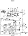
- a semiconductor thin film deposition apparatus includes at least one reactor 100 in which a wafer (not shown) is received, an exhaust pump 200 for exhausting gas from the reactor 100, an ozone supply portion 300 for generating ozone that is supplied to the reactor 100, and a gas supply portion 400 for generating a reaction gas or inert gas that is supplied to the reactor 100.
- This thin film deposition apparatus uses ozone for being reacted with the reaction gas to deposit a thin film on a wafer.
- the semiconductor thin film deposition apparatus may further include a heater (not shown) as a thermal treatment means for performing thermal treatment on a wafer received in the reactor 100.
- the heater can control the temperature of the reactor in a range of 300 to 700 °C.
- the ozone supply portion 300 includes an ozone generator 310, a main valve 320 connected to the ozone generator 310 for allowing ozone to flow or for blocking the flow of ozone, an ozone transfer unit 330 for transferring ozone, which has passed through the main valve 320, to the reactor 100, and an ozone control unit 340 for allowing a certain amount of ozone to flow to the ozone transfer unit 330 when an excessive amount of ozone is generated by the ozone generator 310.
- the ozone transfer unit 330 for guiding ozone generated by the ozone generator 310 to the reactor 100, is designed so that ozone used in a thin film deposition process for a wafer received within the reactor 100 is transferred separately from ozone used in thermal treatment on the wafer. That is, the ozone transfer unit 330 is connected to the main valve 320 in parallel, and includes a process ozone transfer member for transferring ozone used for a thin film deposition process, a thermal treatment ozone transfer member for transferring ozone used for thermal treatment.
- a selection transfer member 339 selectively transfers ozone which has passed through the process ozone transfer member or thermal treatment ozone transfer member, to the reactor 100 or exhaust pump 200. In FIG. 1, two ozone transfer units are shown. However, the other transfer unit will not be described because it has the same structure as the above-described ozone transfer unit 330. If several ozone transfer units described above are used, an equal number of reactors can be operated.
- the process ozone transfer member is made up of a first process valve 332, a process mass flow controller (MFC1), and a second process valve 334, which are sequentially connected.
- MFC1 process mass flow controller
- the thermal treatment ozone transfer member is made up of a first thermal treatment valve 336, a thermal treatment mass flow controller (MFC2), and a second thermal treatment valve 338, which are sequentially connected.
- MFC2 thermal treatment mass flow controller
- the selection transfer member 339 is made up of a first selection valve 339a and a second selection valve 339b.
- the first selection valve 339a is connected to a line between the second process valve 334 and the second thermal treatment valve 338, and the reactor 100, and allows or blocks the flow of ozone to the reactor 100.
- the second selection valve 339b is connected to a line between the second process valve 334 and the second thermal treatment valve 338, and the exhaust pump 200, and allows or blocks the flow of ozone to the exhaust pump 200. If the second selection valve 339b is opened, ozone which has passed through the second process valve 334 and the second thermal treatment valve 338 is applied to the exhaust pump 200.
- the first and second selection valves 339a and 339b perform opposite operations at the same time. That is, when the first selection valve 339a is turned off, the second selection valve 339b is turned on, and vice versa.
- the process MFC1 and the thermal treatment MFC2 control the flow of ozone.
- the process MFC1 controls the flow of ozone used in a thin film deposition process in a range of 100 to 500 sccm (standard cc/min).
- the thermal treatment MFC2 controls the flow of ozone used for thermal treatment up to 20000 sccm.
- ozone generator 310 It is not easy to control the amount of ozone generated by the ozone generator 310 in an the exact amount actually used in a thin film deposition process or thermal treatment. In practice, a small amount of ozone is used in a deposition process or thermal treatment process. However, the ozone generator 310 generally generates an excessive amount. Thus, a high ozone pressure is applied to a line connected between the ozone generator 310 and the main valve 320. When an excessive ozone pressure is applied to the line, even the MFC1 and MFC2 cannot properly control the flow of ozone. In this case, the ozone control unit 340 is operated.
- the ozone control unit 340 includes an automatic pressure valve 341 and an ozone remover 342 which are installed on the line between the main valve 320 and the ozone generator 310.
- the automatic pressure valve 341 is automatically opened when the ozone pressure is equal to or greater than a predetermined value, and the ozone remover 342 removes ozone which has passed through the automatic pressure valve 341.
- the ozone remover 342 can be a catalyzer that converts harmful ozone to harmless oxygen or another gas through a catalyzed chemical reaction and then exhausts the resultant gas.
- the ozone control unit 340 further includes a valve 345 and a check valve 344 which are installed on the line between the main valve 320 and the ozone remover 342.
- the valve 345 allows/blocks the flow of ozone
- the check valve 344 allows ozone having a predetermined pressure or greater to flow only toward the ozone remover 342.
- the pressure is fed back to operate the ozone control unit 340. That is, when the ozone pressure is equal to or greater than a predetermined value, the pressure valve 341 is opened, so that a superfluous amount of ozone flows toward the ozone remover 342. Also, in the ozone remover 342, the introduced ozone is converted into harmless gas by a catalyst, and then the harmless gas is exhausted.
- the ozone control unit 340 can maintain the pressure of ozone flowing into the ozone transfer unit 330 to be uniform, and thus can guide ozone at a stable state.
- ozone generated by the ozone generator 310 flows into the reactor 100 along a route starting from the main valve 320 to the first process valve 332, to the process MFC1, to the second process valve 334, to the first selection valve 339a, or along a route starting from the main valve 320 to the first thermal treatment valve 336, to the thermal treatment MFC2, to the second thermal treatment valve 338, to the first selection valve 339a. That is, ozone can be selectively allowed to flow into the reactor 100 by selectively turning on or off the first process valve 332 or the first thermal treatment valve 336.
- the first and second selection valves 339a and 339b perform opposite operations at the same time, so that when the first selection valve 339a is turned off, the second selection valve 339b is turned on. Hence, ozone is exhausted directly to the outside by the exhaust pump 200.
- the gas supply portion 400 includes a first reaction gas supply unit 410 for supplying a first reaction gas to the reactor 100, a second reaction gas supply unit 420 for supplying a second reaction gas, and an inert gas supply unit 430 for supplying an inert gas used as a carrier gas or a purging gas.
- the first and second reaction gas supply units 410 and 420, and the inert gas supply unit 430 are connected to each other by a pipe line, and several valves 411, 412, 413, 414, 415, 421, 422, 423, 424 and 425 are installed on the line. These valves are connected to a controller (not shown) to allow/block the flow of gas.
- the first reaction gas supply unit 410 includes a first reaction material container 416 filled with a first liquid reaction material to be vaporized and used as a first reaction gas, a mass flow controller (MFC) for controlling the flow of a carrier gas for transferring the first reaction gas to the reactor 100, a first flow control valve 412a installed between the first reaction material container 416 and a valve 412, and a second flow control valve 414a installed between the MFC and the valve 414.
- the first and second flow control valves 412a and 414a consecutively control the flow of gas, and uniformly raise/maintain the vapor pressure of a gas introduced into the reactor 100.
- argon is used as the inert carrier gas.
- various inert gases such as neon can be used instead of argon.
- the second reaction gas supply unit 420 includes a second reaction material container 426 filled with a second liquid reaction material to be vaporized and used as a second reaction gas, an MFC for controlling the flow of a carrier gas for transferring the second reaction gas to the reactor 100, a first flow control valve 422a installed between the second reaction material container 426 and the valve 422, and a second flow control valve 424a installed between the MFC and the valve 424.
- the first and second flow control valves 422a and 424a consecutively control the flow of gas, and uniformly raise/maintain the vapor pressure of a gas introduced into the reactor 100.
- first and second flow control valves 412a, 414a, 422a and 424a adopted in the first and second gas supply units 410 and 420 are meter valves or control valves. It is also preferable that the first and second flow control valves 412a, 414a, 422a and 424a are installed in front of the valves 412, 414, 422 and 424, and that the distance between a flow control valve and an adjacent valve is minimized in order to control the flow of gas at a stable constant pressure.
- the flow control valves 412a, 414a, 422a and 424a control the flow of gas by adjusting the cross-sectional area through which gas passes.
- a transfer gas introduced via a first supply line 41 and the valve 411 flows into the reactor 100 via a route from the flow control valve 412a, to the valves 412 and 413, to a reactor line 45, together with the first reaction gas of the first reaction material container 416.
- valves 414 and 415 are opened, a carrier gas introduced via the first supply line 41 is exhausted to the outside through a route from the second flow control valve 414a, to the valves 414 and 415, to an exhaust line 46, to the exhaust pump 200.
- the first and second flow control valves 412a and 414a consecutively control the flow of gas, uniformly raise/maintain the vapor pressure of a gas flowing into the reactor 100, and equalize the pressure of a gas applied to the reactor 100 with the pressure of a gas applied to the exhaust pump 200.
- an inert gas flows into the reactor 100 along a route from the valve 431 to the valve 432 to the reactor line 45, and exhausts a reaction gas that remains within the reactor 100.
- the second reaction gas of the second reaction material container 426 is allowed to flow into the reactor 100 via a route from the first flow amount control valve 422a, to the valves 422 and 423, to the reactor line 45, along with the carrier gas introduced via a second supply line 42 and the valve 421. Then, if the valves 424 and 425 are opened, the carrier gas is exhausted to the outside via the route from the second flow amount control valve 424a, to the valves 424 and 425, to the exhaust line 46, to the exhaust pump 200.
- the first and second flow control valves 422a and 424a consecutively control the flow of gas, uniformly raise/maintain the vapor pressure of a gas flowing into the reactor 100, and equalize the pressure of a gas applied to the reactor 100 with the pressure of a gas applied to the exhaust pump 200.
- An inert gas flows into the reactor 100 along a route from the valve 431 to the valve 432 to the reactor line 45, and exhausts a reaction gas that remains within the reactor 100.
- thermal treatment using ozone is performed as a pre-process for easily depositing a thin film on a wafer.
- the internal temperature of the reactor 100 is increased to a range of 300 to 700 degreesC, and ozone is supplied into the reactor 100.
- ozone generated by the ozone generator 310 is introduced into the reactor 100 via a route from the main valve 320, to the first thermal treatment valve 336, to the thermal treatment MFC2, to the second thermal treatment valve 338, and to the first selection valve 339a. It is preferable that the thermal treatment is performed at a temperature as high as possible to accelerate decomposition of ozone.
- ozone and a reaction gas flow into a reactor at the same time or a time interval apart, in order to deposit an aluminum oxide film on a wafer. That is, ozone generated by the ozone generator 310 flows into the reactor 100 via a route from the main valve 320, to the first process valve 332, to the process MFC1, to the second process valve 334, and to the selection valve 339a. Meanwhile, the first reaction gas of the first reaction material container 416 flows into the reactor 100 via a route from the flow control valve 412a, to the valves 412 and 413, and to the reactor line 45 along with a carrier gas introduced via the first supply line 41 and the valve 411, as the valves 411, 412 and 413 are opened. The ozone and the first reaction gas flowing into the reactor 100 react with each other, so that an aluminum oxide film is deposited on the wafer.
- an inert gas flows into the reactor 100 via a route from the valve 431, to the valve 432 and to the reactor line 45 to exhaust the ozone and first reaction gas within the reactor 100.
- a thin film deposition process is continuously performed by supplying the second reaction gas of the second reaction material container 426, together with ozone, into the reactor 100 through a similar operation to that described above.
- a thin film can be deposited at a thickness of an atomic layer by varying the inflow duration of a reaction gas or ozone. Also, an inert gas for purging is allowed to flow into the reactor between the times for introducing ozone and a reaction gas.
- the internal temperature of the reactor is increased to a range of 300 to 700 degreesC, and ozone is supplied into the reactor. In this way, thermal treatment is performed.
- the flow of ozone is made equal to those of the first and second reaction gases, in order to suppress a change in the pressure of a reactor due to the sequential inflow of ozone and first and second reaction gases.
- a defectless thin film can be formed on a wafer using ozone instead of deionized (DI) water vapor for oxidation as in the prior art. That is, in contrast to the prior art, generation of an H group that can permeate into a thin film is prevented, so that defects in a thin film caused by H can be prevented.
- DI deionized
- thermal treatment can be performed together with a thin film deposition process, leading to deposition of a high-quality thin film and a simple process.
Landscapes
- Chemical & Material Sciences (AREA)
- General Chemical & Material Sciences (AREA)
- Chemical Kinetics & Catalysis (AREA)
- Engineering & Computer Science (AREA)
- Materials Engineering (AREA)
- Mechanical Engineering (AREA)
- Metallurgy (AREA)
- Organic Chemistry (AREA)
- Electrochemistry (AREA)
- Chemical Vapour Deposition (AREA)
- Formation Of Insulating Films (AREA)
- Physical Deposition Of Substances That Are Components Of Semiconductor Devices (AREA)
- Physical Vapour Deposition (AREA)
- Crystals, And After-Treatments Of Crystals (AREA)
- Internal Circuitry In Semiconductor Integrated Circuit Devices (AREA)
- Magnetic Heads (AREA)
Claims (11)
- Vorrichtung zum Aufbringen dünner Halbleiterschichten mit:wobei der Ozonversorgungsabschnitt (300) aufweist:wenigstens einem Reaktor (100), in den ein Wafer aufgenommen wird,einem Gasversorgungsabschnitt (400) zum Zuführen eines Reaktionsgases oder eines Inertgases zu dem Reaktor, wobei der Gasversorgungsabschnitt (400) aufweist:wenigstens eine Reaktionsgasversorgungseinheit (410, 420) zum selektiven Liefern von Reaktionsgas zu dem Reaktor (100), undeiner Inertgasversorgungseinheit (430) zum Liefern des Inertgases zu dem Reaktor (100),einer Entlüftungspumpe (200) zum Entlüften von Gas aus dem Reaktor (200),einem Ozonversorgungsabschnitt (300) zum Erzeugen von Ozon zur Reaktion mit dem Reaktionsgas,einer selektiven Transfereinheit (339) zum selektiven Überführen von Ozon, das von der wenigstens einen Ozontransfereinheit (330) geliefert wird, zu dem Reaktor (100) oder zu der Entlüftungspumpe (200).einen Ozongenerator (210) zum Erzeugen des Ozons,ein Hauptventil (320), um Ozon fließen zu lassen oder um den Fluss des Ozons zu blockieren,wenigstens eine Ozontransfereinheit (330) mit zwei Massenstromreglern (MFC1, MFC2) zum Überführen von Ozon zu dem Reaktor (100) mit zwei verschiedenen Stromwerten, undeine Überschussozonsteuereinheit (340) zum Entfernen von Ozon, wenn von dem Ozongenerator eine Ozonmenge erzeugt ist, die diejenige übersteigt, die für den von der Ozontransfereinheit überführten Stromwert erforderlich ist, und
- Vorrichtung zum Aufbringen dünner Halbleiterschichten nach Anspruch 1, wobei die Ozontransfereinheit (330) aufweist:eine Prozessozon-Transfereinheit zum Überführen von in einem Dünnschichtaufbringungsprozess verwendetem Ozon, undeine Wärmebehandlungsozon-Transfereinheit zum Überführen von Ozon, das in einem Wärmebehandlungsprozess verwendet wird.
- Vorrichtung zum Aufbringen von dünnen Halbleiterschichten nach Anspruch 1 oder 2, wobei die selektive Transfereinheit aufweist:ein erstes Selektionsventil, das mit einer Leitung zwischen der Prozessozon-Transfereinheit und der Wärmebehandlungsozon-Transfereinheit und dem Reaktor verbunden ist, undein zweites Selektionsventil, das mit der Leitung und der Entlüftungspumpe verbunden ist.
- Vorrichtung zum Aufbringen dünner Halbleiterschichten nach Anspruch 2, wobei die Prozessozon-Transfereinheit aufweist:wobei der Prozessmassenstromregler den Ozonstrom auf einen ersten Stromwert regelt.ein erstes Prozessventil, das mit dem Hauptventil in Reihe verbunden ist,einen Prozessmassenstromregler, undein zweites Prozessventil, das in Reihe mit dem Prozessmassenstromregler und dem ersten Prozessventil verbunden ist,
- Vorrichtung zum Aufbringen dünner Halbleiterschichten nach Anspruch 4, wobei der erste Stromwert bis zu 500 sccm beträgt.
- Vorrichtung zum Aufbringen dünner Halbleiterschichten nach Anspruch 2, wobei die Wärmebehandlungsozon-Transfereinheit aufweist:wobei der Wärmebehandlungsmassenstromregler vorzugsweise den Ozonstrom auf einen zweiten Stromwert regelt.ein erstes Wärmebehandlungsventil, das mit dem Hauptventil in Reihe damit verbunden ist,einen Wärmebehandlungsmassenstromsregler, undein zweites Wärmebehandlungsventil, das in Aufeinanderfolge mit dem Wärmebehandlungsmassenstromregler und dem ersten Wärmebehandlungsventil verbunden ist,
- Vorrichtung zum Aufbringen dünner Halbleiterschichten nach Anspruch 6, wobei der zweite Stromwert bis zu 20 000 sccm beträgt.
- Vorrichtung zum Aufbringen dünner Halbleiterschichten nach Anspruch 2, wobei die Überschussozonsteuereinheit ein automatisches Druckventil und einen Ozonentferner umfasst, die an der Leitung zwischen dem Hauptventil und dem Ozongenerator installiert sind, und wobei das automatische Druckventil automatisch geöffnet wird, wenn der Ozondruck gleich oder größer als ein vorgegebener Wert ist, und wobei der Ozonentferner Ozon entfernt, das durch das automatische Druckventil geflossen ist.
- Vorrichtung zum Aufbringen dünner Halbleiterschichten nach Anspruch 8, wobei die Überschussozonsteuereinheit weiter ein Ventil zum Durchlass/Blockieren des Ozonstroms und ein Rückschlagventil zum Durchlassen von Ozon, das einen vorgegebenen Druck oder höher hat, um es ausschließlich zu dem Ozonentferner fließen zu lassen, aufweist, wobei das Ventil und das Rückschlagventil an der Leitung zwischen dem Hauptventil und dem Ozonentferner installiert sind.
- Vorrichtung zum Aufbringen dünner Halbleiterschichten nach Anspruch 1, die weiter eine Heizung zum Erreichen einer Temperatur aufweist, um eine Wärmebehandlung des in dem Reaktor aufgenommenen Wafers in dem Reaktor durchzuführen, und wobei vorzugsweise die Heizung die Temperatur in einem Bereich von 300 - 700°C einstellt.
- Vorrichtung zum Aufbringen dünner Halbleiterschichten nach Anspruch 1, wobei das Inertgas Argon ist.
Applications Claiming Priority (2)
| Application Number | Priority Date | Filing Date | Title |
|---|---|---|---|
| KR9958541 | 1999-12-17 | ||
| KR1019990058541A KR100330749B1 (ko) | 1999-12-17 | 1999-12-17 | 반도체 박막증착장치 |
Publications (2)
| Publication Number | Publication Date |
|---|---|
| EP1108468A1 EP1108468A1 (de) | 2001-06-20 |
| EP1108468B1 true EP1108468B1 (de) | 2004-06-02 |
Family
ID=19626555
Family Applications (1)
| Application Number | Title | Priority Date | Filing Date |
|---|---|---|---|
| EP00311218A Expired - Lifetime EP1108468B1 (de) | 1999-12-17 | 2000-12-15 | Vorrichtung zum Aufbringen von dünnen Schichten |
Country Status (8)
| Country | Link |
|---|---|
| US (1) | US6740166B2 (de) |
| EP (1) | EP1108468B1 (de) |
| JP (1) | JP3481586B2 (de) |
| KR (1) | KR100330749B1 (de) |
| AT (1) | ATE268217T1 (de) |
| DE (1) | DE60011215T2 (de) |
| SG (1) | SG98002A1 (de) |
| TW (1) | TW466565B (de) |
Families Citing this family (68)
| Publication number | Priority date | Publication date | Assignee | Title |
|---|---|---|---|---|
| DE10063717C1 (de) | 2000-12-20 | 2002-02-21 | Infineon Technologies Ag | Verfahren zur Abscheidung dünner Schichten durch Chemical Vapor Deposition |
| US6998579B2 (en) | 2000-12-29 | 2006-02-14 | Applied Materials, Inc. | Chamber for uniform substrate heating |
| US6765178B2 (en) | 2000-12-29 | 2004-07-20 | Applied Materials, Inc. | Chamber for uniform substrate heating |
| US6825447B2 (en) | 2000-12-29 | 2004-11-30 | Applied Materials, Inc. | Apparatus and method for uniform substrate heating and contaminate collection |
| US6660126B2 (en) | 2001-03-02 | 2003-12-09 | Applied Materials, Inc. | Lid assembly for a processing system to facilitate sequential deposition techniques |
| US6878206B2 (en) | 2001-07-16 | 2005-04-12 | Applied Materials, Inc. | Lid assembly for a processing system to facilitate sequential deposition techniques |
| KR100420117B1 (ko) * | 2001-03-12 | 2004-03-02 | 삼성전자주식회사 | 수소 확산방지막을 포함하는 반도체 장치 및 그 제조 방법 |
| US6849545B2 (en) | 2001-06-20 | 2005-02-01 | Applied Materials, Inc. | System and method to form a composite film stack utilizing sequential deposition techniques |
| US20030198754A1 (en) * | 2001-07-16 | 2003-10-23 | Ming Xi | Aluminum oxide chamber and process |
| US9051641B2 (en) | 2001-07-25 | 2015-06-09 | Applied Materials, Inc. | Cobalt deposition on barrier surfaces |
| JP2005504885A (ja) | 2001-07-25 | 2005-02-17 | アプライド マテリアルズ インコーポレイテッド | 新規なスパッタ堆積方法を使用したバリア形成 |
| US8110489B2 (en) | 2001-07-25 | 2012-02-07 | Applied Materials, Inc. | Process for forming cobalt-containing materials |
| US20090004850A1 (en) | 2001-07-25 | 2009-01-01 | Seshadri Ganguli | Process for forming cobalt and cobalt silicide materials in tungsten contact applications |
| US20030029715A1 (en) | 2001-07-25 | 2003-02-13 | Applied Materials, Inc. | An Apparatus For Annealing Substrates In Physical Vapor Deposition Systems |
| US7085616B2 (en) | 2001-07-27 | 2006-08-01 | Applied Materials, Inc. | Atomic layer deposition apparatus |
| US6718126B2 (en) | 2001-09-14 | 2004-04-06 | Applied Materials, Inc. | Apparatus and method for vaporizing solid precursor for CVD or atomic layer deposition |
| US7049226B2 (en) | 2001-09-26 | 2006-05-23 | Applied Materials, Inc. | Integration of ALD tantalum nitride for copper metallization |
| US6936906B2 (en) | 2001-09-26 | 2005-08-30 | Applied Materials, Inc. | Integration of barrier layer and seed layer |
| US7780785B2 (en) | 2001-10-26 | 2010-08-24 | Applied Materials, Inc. | Gas delivery apparatus for atomic layer deposition |
| US6916398B2 (en) | 2001-10-26 | 2005-07-12 | Applied Materials, Inc. | Gas delivery apparatus and method for atomic layer deposition |
| US6773507B2 (en) * | 2001-12-06 | 2004-08-10 | Applied Materials, Inc. | Apparatus and method for fast-cycle atomic layer deposition |
| US6729824B2 (en) | 2001-12-14 | 2004-05-04 | Applied Materials, Inc. | Dual robot processing system |
| WO2003065424A2 (en) | 2002-01-25 | 2003-08-07 | Applied Materials, Inc. | Apparatus for cyclical deposition of thin films |
| US6866746B2 (en) * | 2002-01-26 | 2005-03-15 | Applied Materials, Inc. | Clamshell and small volume chamber with fixed substrate support |
| US6911391B2 (en) | 2002-01-26 | 2005-06-28 | Applied Materials, Inc. | Integration of titanium and titanium nitride layers |
| US6998014B2 (en) | 2002-01-26 | 2006-02-14 | Applied Materials, Inc. | Apparatus and method for plasma assisted deposition |
| US6972267B2 (en) | 2002-03-04 | 2005-12-06 | Applied Materials, Inc. | Sequential deposition of tantalum nitride using a tantalum-containing precursor and a nitrogen-containing precursor |
| US7186385B2 (en) | 2002-07-17 | 2007-03-06 | Applied Materials, Inc. | Apparatus for providing gas to a processing chamber |
| US6955211B2 (en) | 2002-07-17 | 2005-10-18 | Applied Materials, Inc. | Method and apparatus for gas temperature control in a semiconductor processing system |
| US7066194B2 (en) * | 2002-07-19 | 2006-06-27 | Applied Materials, Inc. | Valve design and configuration for fast delivery system |
| US6772072B2 (en) | 2002-07-22 | 2004-08-03 | Applied Materials, Inc. | Method and apparatus for monitoring solid precursor delivery |
| US6915592B2 (en) | 2002-07-29 | 2005-07-12 | Applied Materials, Inc. | Method and apparatus for generating gas to a processing chamber |
| JP4303925B2 (ja) | 2002-08-19 | 2009-07-29 | 篠田プラズマ株式会社 | 金属酸化膜の形成方法及びガス放電管の2次電子放出膜形成方法 |
| US6821563B2 (en) | 2002-10-02 | 2004-11-23 | Applied Materials, Inc. | Gas distribution system for cyclical layer deposition |
| US20040069227A1 (en) | 2002-10-09 | 2004-04-15 | Applied Materials, Inc. | Processing chamber configured for uniform gas flow |
| US6905737B2 (en) | 2002-10-11 | 2005-06-14 | Applied Materials, Inc. | Method of delivering activated species for rapid cyclical deposition |
| EP1420080A3 (de) | 2002-11-14 | 2005-11-09 | Applied Materials, Inc. | Vorrichtung und Verfahren zu hybriden chemischen Abscheidungsverfahren |
| US6868859B2 (en) * | 2003-01-29 | 2005-03-22 | Applied Materials, Inc. | Rotary gas valve for pulsing a gas |
| US6994319B2 (en) * | 2003-01-29 | 2006-02-07 | Applied Materials, Inc. | Membrane gas valve for pulsing a gas |
| US20040177813A1 (en) | 2003-03-12 | 2004-09-16 | Applied Materials, Inc. | Substrate support lift mechanism |
| DE10325629A1 (de) * | 2003-03-21 | 2004-10-07 | Forschungszentrum Jülich GmbH | Verfahren zur Abscheidung von Verbindungen auf einem Substrat mittels metallorganischer Gasphasendeposition |
| US20070031991A1 (en) * | 2003-03-21 | 2007-02-08 | Forschungszentrum Julich Gmbh | Method for depositing compounds on a substrate by means of metalorganic chemical vapor deposition |
| US7342984B1 (en) | 2003-04-03 | 2008-03-11 | Zilog, Inc. | Counting clock cycles over the duration of a first character and using a remainder value to determine when to sample a bit of a second character |
| US20040198069A1 (en) | 2003-04-04 | 2004-10-07 | Applied Materials, Inc. | Method for hafnium nitride deposition |
| KR100505064B1 (ko) | 2003-05-06 | 2005-07-29 | 삼성전자주식회사 | 반도체 소자의 산화방법 및 이를 이용한 산화막 형성방법 |
| US20050067103A1 (en) * | 2003-09-26 | 2005-03-31 | Applied Materials, Inc. | Interferometer endpoint monitoring device |
| US20050252449A1 (en) | 2004-05-12 | 2005-11-17 | Nguyen Son T | Control of gas flow and delivery to suppress the formation of particles in an MOCVD/ALD system |
| US8119210B2 (en) | 2004-05-21 | 2012-02-21 | Applied Materials, Inc. | Formation of a silicon oxynitride layer on a high-k dielectric material |
| US8323754B2 (en) | 2004-05-21 | 2012-12-04 | Applied Materials, Inc. | Stabilization of high-k dielectric materials |
| US7402534B2 (en) | 2005-08-26 | 2008-07-22 | Applied Materials, Inc. | Pretreatment processes within a batch ALD reactor |
| US7464917B2 (en) | 2005-10-07 | 2008-12-16 | Appiled Materials, Inc. | Ampoule splash guard apparatus |
| KR101019293B1 (ko) | 2005-11-04 | 2011-03-07 | 어플라이드 머티어리얼스, 인코포레이티드 | 플라즈마-강화 원자층 증착 장치 및 방법 |
| KR100725098B1 (ko) * | 2005-11-17 | 2007-06-04 | 삼성전자주식회사 | 반도체 제조설비의 유량조절기 오동작 감지장치 및 그 방법 |
| US20070151668A1 (en) | 2006-01-04 | 2007-07-05 | Tokyo Electron Limited | Gas supply system, substrate processing apparatus, and gas supply method |
| US7798096B2 (en) | 2006-05-05 | 2010-09-21 | Applied Materials, Inc. | Plasma, UV and ion/neutral assisted ALD or CVD in a batch tool |
| US7601648B2 (en) | 2006-07-31 | 2009-10-13 | Applied Materials, Inc. | Method for fabricating an integrated gate dielectric layer for field effect transistors |
| US20080176149A1 (en) * | 2006-10-30 | 2008-07-24 | Applied Materials, Inc. | Endpoint detection for photomask etching |
| US20080099436A1 (en) * | 2006-10-30 | 2008-05-01 | Michael Grimbergen | Endpoint detection for photomask etching |
| US7775508B2 (en) | 2006-10-31 | 2010-08-17 | Applied Materials, Inc. | Ampoule for liquid draw and vapor draw with a continuous level sensor |
| US8821637B2 (en) | 2007-01-29 | 2014-09-02 | Applied Materials, Inc. | Temperature controlled lid assembly for tungsten nitride deposition |
| US8297223B2 (en) * | 2007-10-02 | 2012-10-30 | Msp Corporation | Method and apparatus for particle filtration and enhancing tool performance in film deposition |
| US8146896B2 (en) | 2008-10-31 | 2012-04-03 | Applied Materials, Inc. | Chemical precursor ampoule for vapor deposition processes |
| US8778204B2 (en) | 2010-10-29 | 2014-07-15 | Applied Materials, Inc. | Methods for reducing photoresist interference when monitoring a target layer in a plasma process |
| US8961804B2 (en) | 2011-10-25 | 2015-02-24 | Applied Materials, Inc. | Etch rate detection for photomask etching |
| US8808559B2 (en) | 2011-11-22 | 2014-08-19 | Applied Materials, Inc. | Etch rate detection for reflective multi-material layers etching |
| US8900469B2 (en) | 2011-12-19 | 2014-12-02 | Applied Materials, Inc. | Etch rate detection for anti-reflective coating layer and absorber layer etching |
| US9805939B2 (en) | 2012-10-12 | 2017-10-31 | Applied Materials, Inc. | Dual endpoint detection for advanced phase shift and binary photomasks |
| US8778574B2 (en) | 2012-11-30 | 2014-07-15 | Applied Materials, Inc. | Method for etching EUV material layers utilized to form a photomask |
Family Cites Families (13)
| Publication number | Priority date | Publication date | Assignee | Title |
|---|---|---|---|---|
| JPS56114809A (en) | 1980-02-12 | 1981-09-09 | Toshiba Corp | Ozonizer |
| JP2888253B2 (ja) * | 1989-07-20 | 1999-05-10 | 富士通株式会社 | 化学気相成長法およびその実施のための装置 |
| JPH04196528A (ja) * | 1990-11-28 | 1992-07-16 | Toshiba Corp | マグネトロンエッチング装置 |
| JPH05247654A (ja) | 1991-03-19 | 1993-09-24 | Babcock Hitachi Kk | 光励起cvd装置 |
| JPH05234882A (ja) | 1992-02-21 | 1993-09-10 | Hitachi Ltd | 表面処理装置 |
| JP3174856B2 (ja) * | 1993-05-07 | 2001-06-11 | 日本エア・リキード株式会社 | 混合ガス供給装置 |
| US5352615A (en) * | 1994-01-24 | 1994-10-04 | Motorola, Inc. | Denuding a semiconductor substrate |
| AU1288197A (en) * | 1995-12-15 | 1997-07-14 | Watkins-Johnson Company | Method of forming dielectric films with reduced metal contamination |
| JPH09232296A (ja) * | 1996-02-23 | 1997-09-05 | Mitsubishi Electric Corp | 半導体装置の製造装置および製造方法 |
| US6004397A (en) * | 1996-05-16 | 1999-12-21 | Lg Semicon Co., Ltd. | TEOS-O3 oxidizing film depositing system and process for supplying ozone (O3) thereto |
| US6277347B1 (en) | 1997-02-24 | 2001-08-21 | Applied Materials, Inc. | Use of ozone in process effluent abatement |
| US5976471A (en) * | 1997-04-16 | 1999-11-02 | Lockheed Martin Energy Systems, Inc. | Ozone decomposing filter |
| US5876798A (en) * | 1997-12-29 | 1999-03-02 | Chartered Semiconductor Manufacturing, Ltd. | Method of fluorinated silicon oxide film deposition |
-
1999
- 1999-12-17 KR KR1019990058541A patent/KR100330749B1/ko not_active Expired - Lifetime
-
2000
- 2000-11-30 US US09/726,977 patent/US6740166B2/en not_active Expired - Fee Related
- 2000-12-07 TW TW089126057A patent/TW466565B/zh not_active IP Right Cessation
- 2000-12-13 JP JP2000378316A patent/JP3481586B2/ja not_active Expired - Fee Related
- 2000-12-13 SG SG200007424A patent/SG98002A1/en unknown
- 2000-12-15 EP EP00311218A patent/EP1108468B1/de not_active Expired - Lifetime
- 2000-12-15 DE DE60011215T patent/DE60011215T2/de not_active Expired - Lifetime
- 2000-12-15 AT AT00311218T patent/ATE268217T1/de not_active IP Right Cessation
Also Published As
| Publication number | Publication date |
|---|---|
| JP3481586B2 (ja) | 2003-12-22 |
| EP1108468A1 (de) | 2001-06-20 |
| DE60011215D1 (de) | 2004-07-08 |
| KR20010056876A (ko) | 2001-07-04 |
| ATE268217T1 (de) | 2004-06-15 |
| JP2001217232A (ja) | 2001-08-10 |
| TW466565B (en) | 2001-12-01 |
| SG98002A1 (en) | 2003-08-20 |
| US6740166B2 (en) | 2004-05-25 |
| KR100330749B1 (ko) | 2002-04-03 |
| DE60011215T2 (de) | 2005-07-07 |
| US20020134307A1 (en) | 2002-09-26 |
Similar Documents
| Publication | Publication Date | Title |
|---|---|---|
| EP1108468B1 (de) | Vorrichtung zum Aufbringen von dünnen Schichten | |
| US12222644B2 (en) | Method of forming an enhanced unexposed photoresist layer | |
| JP7420744B2 (ja) | 浸透性材料に浸透させる浸透装置および方法 | |
| US6905549B2 (en) | Vertical type semiconductor device producing apparatus | |
| EP1038048B1 (de) | Gaszuführsystem für cvd reaktor und verfahren zu dessen steuerung | |
| CN110858554A (zh) | 衬底处理设备和方法 | |
| US7163719B2 (en) | Method of depositing thin film using hafnium compound | |
| KR20120028305A (ko) | 기판상에 박막을 성장시키는 방법 및 장치 | |
| KR20120126012A (ko) | 가스 공급 장치, 열처리 장치, 가스 공급 방법 및 열처리 방법 | |
| JP2012184499A (ja) | 半導体装置の製造方法、基板処理装置、及び基板処理方法 | |
| JP2009016799A (ja) | 基板処理装置 | |
| WO2005017987A1 (ja) | 基板処理装置及び半導体デバイスの製造方法 | |
| JP4356943B2 (ja) | 基板処理装置及び半導体装置の製造方法 | |
| CN109321897B (zh) | 一种原子层沉积系统及方法 | |
| JP2012015344A (ja) | 半導体装置の製造方法 | |
| KR20040061093A (ko) | 반도체 박막 증착장치 | |
| JP2014154751A (ja) | ガス供給系及び成膜装置 | |
| JP2006222265A (ja) | 基板処理装置 | |
| JP4465398B2 (ja) | 基板処理装置 | |
| US20250006490A1 (en) | Substrate processing method, method of manufacturing semiconductor device, non-transitory computer-readable recording medium and substrate processing apparatus | |
| JP2006066557A (ja) | 基板処理装置 | |
| EP4585714A2 (de) | Verfahren zur substratverarbeitung, verfahren zur herstellung eines halbleiterbauelements, programm und substratverarbeitungsvorrichtung | |
| US20240363334A1 (en) | Method of processing substrate, method of manufacturing semiconductor device, recording medium, and substrate processing apparatus | |
| WO2024154233A1 (ja) | 基板処理方法、半導体装置の製造方法、基板処理装置及びプログラム | |
| KR100230181B1 (ko) | 반도체 제조 장치 및 이를 이용한 반도체 장치의 제조 방법 |
Legal Events
| Date | Code | Title | Description |
|---|---|---|---|
| PUAI | Public reference made under article 153(3) epc to a published international application that has entered the european phase |
Free format text: ORIGINAL CODE: 0009012 |
|
| 17P | Request for examination filed |
Effective date: 20001227 |
|
| AK | Designated contracting states |
Kind code of ref document: A1 Designated state(s): AT BE CH CY DE DK ES FI FR GB GR IE IT LI LU MC NL PT SE TR |
|
| AX | Request for extension of the european patent |
Free format text: AL;LT;LV;MK;RO;SI |
|
| AKX | Designation fees paid |
Free format text: AT BE CH CY DE DK ES FI FR GB GR IE IT LI LU MC NL PT SE TR |
|
| 17Q | First examination report despatched |
Effective date: 20021111 |
|
| GRAP | Despatch of communication of intention to grant a patent |
Free format text: ORIGINAL CODE: EPIDOSNIGR1 |
|
| GRAS | Grant fee paid |
Free format text: ORIGINAL CODE: EPIDOSNIGR3 |
|
| GRAA | (expected) grant |
Free format text: ORIGINAL CODE: 0009210 |
|
| AK | Designated contracting states |
Kind code of ref document: B1 Designated state(s): AT BE CH CY DE DK ES FI FR GB GR IE IT LI LU MC NL PT SE TR |
|
| PG25 | Lapsed in a contracting state [announced via postgrant information from national office to epo] |
Ref country code: IT Free format text: LAPSE BECAUSE OF FAILURE TO SUBMIT A TRANSLATION OF THE DESCRIPTION OR TO PAY THE FEE WITHIN THE PRESCRIBED TIME-LIMIT;WARNING: LAPSES OF ITALIAN PATENTS WITH EFFECTIVE DATE BEFORE 2007 MAY HAVE OCCURRED AT ANY TIME BEFORE 2007. THE CORRECT EFFECTIVE DATE MAY BE DIFFERENT FROM THE ONE RECORDED. Effective date: 20040602 Ref country code: AT Free format text: LAPSE BECAUSE OF FAILURE TO SUBMIT A TRANSLATION OF THE DESCRIPTION OR TO PAY THE FEE WITHIN THE PRESCRIBED TIME-LIMIT Effective date: 20040602 Ref country code: FI Free format text: LAPSE BECAUSE OF FAILURE TO SUBMIT A TRANSLATION OF THE DESCRIPTION OR TO PAY THE FEE WITHIN THE PRESCRIBED TIME-LIMIT Effective date: 20040602 Ref country code: NL Free format text: LAPSE BECAUSE OF FAILURE TO SUBMIT A TRANSLATION OF THE DESCRIPTION OR TO PAY THE FEE WITHIN THE PRESCRIBED TIME-LIMIT Effective date: 20040602 Ref country code: BE Free format text: LAPSE BECAUSE OF FAILURE TO SUBMIT A TRANSLATION OF THE DESCRIPTION OR TO PAY THE FEE WITHIN THE PRESCRIBED TIME-LIMIT Effective date: 20040602 Ref country code: CY Free format text: LAPSE BECAUSE OF FAILURE TO SUBMIT A TRANSLATION OF THE DESCRIPTION OR TO PAY THE FEE WITHIN THE PRESCRIBED TIME-LIMIT Effective date: 20040602 Ref country code: LI Free format text: LAPSE BECAUSE OF FAILURE TO SUBMIT A TRANSLATION OF THE DESCRIPTION OR TO PAY THE FEE WITHIN THE PRESCRIBED TIME-LIMIT Effective date: 20040602 Ref country code: CH Free format text: LAPSE BECAUSE OF FAILURE TO SUBMIT A TRANSLATION OF THE DESCRIPTION OR TO PAY THE FEE WITHIN THE PRESCRIBED TIME-LIMIT Effective date: 20040602 Ref country code: TR Free format text: LAPSE BECAUSE OF FAILURE TO SUBMIT A TRANSLATION OF THE DESCRIPTION OR TO PAY THE FEE WITHIN THE PRESCRIBED TIME-LIMIT Effective date: 20040602 |
|
| REG | Reference to a national code |
Ref country code: GB Ref legal event code: FG4D |
|
| RIN1 | Information on inventor provided before grant (corrected) |
Inventor name: WON-SUNG, CHOI |
|
| REG | Reference to a national code |
Ref country code: CH Ref legal event code: EP |
|
| REF | Corresponds to: |
Ref document number: 60011215 Country of ref document: DE Date of ref document: 20040708 Kind code of ref document: P |
|
| REG | Reference to a national code |
Ref country code: IE Ref legal event code: FG4D |
|
| PG25 | Lapsed in a contracting state [announced via postgrant information from national office to epo] |
Ref country code: SE Free format text: LAPSE BECAUSE OF FAILURE TO SUBMIT A TRANSLATION OF THE DESCRIPTION OR TO PAY THE FEE WITHIN THE PRESCRIBED TIME-LIMIT Effective date: 20040902 Ref country code: DK Free format text: LAPSE BECAUSE OF FAILURE TO SUBMIT A TRANSLATION OF THE DESCRIPTION OR TO PAY THE FEE WITHIN THE PRESCRIBED TIME-LIMIT Effective date: 20040902 Ref country code: GR Free format text: LAPSE BECAUSE OF FAILURE TO SUBMIT A TRANSLATION OF THE DESCRIPTION OR TO PAY THE FEE WITHIN THE PRESCRIBED TIME-LIMIT Effective date: 20040902 |
|
| PG25 | Lapsed in a contracting state [announced via postgrant information from national office to epo] |
Ref country code: ES Free format text: LAPSE BECAUSE OF FAILURE TO SUBMIT A TRANSLATION OF THE DESCRIPTION OR TO PAY THE FEE WITHIN THE PRESCRIBED TIME-LIMIT Effective date: 20040913 |
|
| REG | Reference to a national code |
Ref country code: CH Ref legal event code: PL |
|
| NLV1 | Nl: lapsed or annulled due to failure to fulfill the requirements of art. 29p and 29m of the patents act | ||
| PG25 | Lapsed in a contracting state [announced via postgrant information from national office to epo] |
Ref country code: GB Free format text: LAPSE BECAUSE OF NON-PAYMENT OF DUE FEES Effective date: 20041215 Ref country code: LU Free format text: LAPSE BECAUSE OF NON-PAYMENT OF DUE FEES Effective date: 20041215 Ref country code: IE Free format text: LAPSE BECAUSE OF NON-PAYMENT OF DUE FEES Effective date: 20041215 |
|
| PG25 | Lapsed in a contracting state [announced via postgrant information from national office to epo] |
Ref country code: MC Free format text: LAPSE BECAUSE OF NON-PAYMENT OF DUE FEES Effective date: 20041231 |
|
| ET | Fr: translation filed | ||
| PLBE | No opposition filed within time limit |
Free format text: ORIGINAL CODE: 0009261 |
|
| STAA | Information on the status of an ep patent application or granted ep patent |
Free format text: STATUS: NO OPPOSITION FILED WITHIN TIME LIMIT |
|
| 26N | No opposition filed |
Effective date: 20050303 |
|
| GBPC | Gb: european patent ceased through non-payment of renewal fee |
Effective date: 20041215 |
|
| REG | Reference to a national code |
Ref country code: IE Ref legal event code: MM4A |
|
| PG25 | Lapsed in a contracting state [announced via postgrant information from national office to epo] |
Ref country code: PT Free format text: LAPSE BECAUSE OF NON-PAYMENT OF DUE FEES Effective date: 20041102 |
|
| PGFP | Annual fee paid to national office [announced via postgrant information from national office to epo] |
Ref country code: FR Payment date: 20061221 Year of fee payment: 7 |
|
| REG | Reference to a national code |
Ref country code: FR Ref legal event code: ST Effective date: 20081020 |
|
| PG25 | Lapsed in a contracting state [announced via postgrant information from national office to epo] |
Ref country code: FR Free format text: LAPSE BECAUSE OF NON-PAYMENT OF DUE FEES Effective date: 20071231 |
|
| REG | Reference to a national code |
Ref country code: DE Ref legal event code: R082 Ref document number: 60011215 Country of ref document: DE Representative=s name: HOFFMANN - EITLE, DE |
|
| REG | Reference to a national code |
Ref country code: DE Ref legal event code: R082 Ref document number: 60011215 Country of ref document: DE Representative=s name: HOFFMANN - EITLE PATENT- UND RECHTSANWAELTE PA, DE Effective date: 20120222 Ref country code: DE Ref legal event code: R081 Ref document number: 60011215 Country of ref document: DE Owner name: WONIK IPS CO., LTD., PYEONGTAEK-SI, KR Free format text: FORMER OWNER: IPS LTD., PYUNGTAEK, KYONGGI, KR Effective date: 20120222 Ref country code: DE Ref legal event code: R082 Ref document number: 60011215 Country of ref document: DE Representative=s name: HOFFMANN - EITLE, DE Effective date: 20120222 Ref country code: DE Ref legal event code: R081 Ref document number: 60011215 Country of ref document: DE Owner name: WONIK IPS CO., LTD., KR Free format text: FORMER OWNER: IPS LTD., PYUNGTAEK, KR Effective date: 20120222 |
|
| PGFP | Annual fee paid to national office [announced via postgrant information from national office to epo] |
Ref country code: DE Payment date: 20131211 Year of fee payment: 14 |
|
| REG | Reference to a national code |
Ref country code: DE Ref legal event code: R119 Ref document number: 60011215 Country of ref document: DE |
|
| PG25 | Lapsed in a contracting state [announced via postgrant information from national office to epo] |
Ref country code: DE Free format text: LAPSE BECAUSE OF NON-PAYMENT OF DUE FEES Effective date: 20150701 |