EP1109221A2 - Structure d'interconnexions de type damascène et son procédé de réalisation - Google Patents
Structure d'interconnexions de type damascène et son procédé de réalisation Download PDFInfo
- Publication number
- EP1109221A2 EP1109221A2 EP00403464A EP00403464A EP1109221A2 EP 1109221 A2 EP1109221 A2 EP 1109221A2 EP 00403464 A EP00403464 A EP 00403464A EP 00403464 A EP00403464 A EP 00403464A EP 1109221 A2 EP1109221 A2 EP 1109221A2
- Authority
- EP
- European Patent Office
- Prior art keywords
- layer
- interconnections
- dielectric material
- sublayer
- sich
- Prior art date
- Legal status (The legal status is an assumption and is not a legal conclusion. Google has not performed a legal analysis and makes no representation as to the accuracy of the status listed.)
- Granted
Links
Images


Classifications
-
- H—ELECTRICITY
- H10—SEMICONDUCTOR DEVICES; ELECTRIC SOLID-STATE DEVICES NOT OTHERWISE PROVIDED FOR
- H10W—GENERIC PACKAGES, INTERCONNECTIONS, CONNECTORS OR OTHER CONSTRUCTIONAL DETAILS OF DEVICES COVERED BY CLASS H10
- H10W20/00—Interconnections in chips, wafers or substrates
- H10W20/01—Manufacture or treatment
- H10W20/071—Manufacture or treatment of dielectric parts thereof
- H10W20/074—Manufacture or treatment of dielectric parts thereof of dielectric parts comprising thin functional dielectric layers, e.g. dielectric etch-stop, barrier, capping or liner layers
- H10W20/075—Manufacture or treatment of dielectric parts thereof of dielectric parts comprising thin functional dielectric layers, e.g. dielectric etch-stop, barrier, capping or liner layers of multilayered thin functional dielectric layers
-
- H—ELECTRICITY
- H10—SEMICONDUCTOR DEVICES; ELECTRIC SOLID-STATE DEVICES NOT OTHERWISE PROVIDED FOR
- H10W—GENERIC PACKAGES, INTERCONNECTIONS, CONNECTORS OR OTHER CONSTRUCTIONAL DETAILS OF DEVICES COVERED BY CLASS H10
- H10W20/00—Interconnections in chips, wafers or substrates
- H10W20/01—Manufacture or treatment
- H10W20/071—Manufacture or treatment of dielectric parts thereof
- H10W20/081—Manufacture or treatment of dielectric parts thereof by forming openings in the dielectric parts
- H10W20/084—Manufacture or treatment of dielectric parts thereof by forming openings in the dielectric parts for dual-damascene structures
- H10W20/086—Manufacture or treatment of dielectric parts thereof by forming openings in the dielectric parts for dual-damascene structures involving buried masks
-
- H—ELECTRICITY
- H10—SEMICONDUCTOR DEVICES; ELECTRIC SOLID-STATE DEVICES NOT OTHERWISE PROVIDED FOR
- H10W—GENERIC PACKAGES, INTERCONNECTIONS, CONNECTORS OR OTHER CONSTRUCTIONAL DETAILS OF DEVICES COVERED BY CLASS H10
- H10W20/00—Interconnections in chips, wafers or substrates
- H10W20/01—Manufacture or treatment
- H10W20/071—Manufacture or treatment of dielectric parts thereof
- H10W20/081—Manufacture or treatment of dielectric parts thereof by forming openings in the dielectric parts
- H10W20/084—Manufacture or treatment of dielectric parts thereof by forming openings in the dielectric parts for dual-damascene structures
- H10W20/087—Manufacture or treatment of dielectric parts thereof by forming openings in the dielectric parts for dual-damascene structures involving multiple stacked pre-patterned masks
-
- H—ELECTRICITY
- H10—SEMICONDUCTOR DEVICES; ELECTRIC SOLID-STATE DEVICES NOT OTHERWISE PROVIDED FOR
- H10W—GENERIC PACKAGES, INTERCONNECTIONS, CONNECTORS OR OTHER CONSTRUCTIONAL DETAILS OF DEVICES COVERED BY CLASS H10
- H10W20/00—Interconnections in chips, wafers or substrates
- H10W20/40—Interconnections external to wafers or substrates, e.g. back-end-of-line [BEOL] metallisations or vias connecting to gate electrodes
- H10W20/45—Interconnections external to wafers or substrates, e.g. back-end-of-line [BEOL] metallisations or vias connecting to gate electrodes characterised by their insulating parts
- H10W20/48—Insulating materials thereof
Definitions
- the present invention relates to a Damascene-type interconnection structure. She also relates to its production process.
- the interconnection structures of integrated circuits are conventionally made in aluminum doped with copper (Al-Cu), the doping rate being of the order of 2 to 4%.
- the process used to achieving these interconnection structures consists of deposit the metal, then engrave it to form the network of interconnections and finally to deposit, overcoat, a dielectric which is used to isolate the lines of metal as well laterally (inter-line insulation) only vertically (inter-level insulation). This process is commonly called “conventional” or "gap fill” (filling of inter-line spaces by the dielectric).
- the network of interconnections is formed by etching trenches in a dielectric with very low permittivity, then by deposition of a metallic nitride barrier layer followed filling the trench with copper. Lastly place, the excess copper and barrier material is removed by polishing to leave only the dielectric between the metal lines.
- CMP chemical mechanical polishing
- the materials SiO 2 , Si 3 N 4 and SiO x N y are usually used because they are already commonly used in the production of integrated circuits. In fact, they are used either at the active area of the circuits as insulators, or at the interconnections as intermetallic dielectrics or as passivation dielectrics. They can be deposited by various but well known techniques: by thermal growth of oxide, by low pressure CVD (LPCVD), by atmospheric CVD (APCVD) or by plasma assisted CVD (PECVD).
- LPCVD low pressure CVD
- APCVD atmospheric CVD
- PECVD plasma assisted CVD
- SiO 2 has good electrical qualities and good etching selectivity with respect to organic materials. However, its properties are insufficient on the other points. If 3 N 4 has good etching selectivity, good resistance to abrasion and to diffusion of copper, but its dielectric constant is high. SiON is intermediate between Si 3 N 4 and SiO 2 . Thus, none of these conventional materials has all of the required properties.
- dielectric interface materials can induce an oxidation of the interface or of the whole matrix of the material with low permittivity and thus degrading its properties: dielectric constant, leakage current, densification with modification of the thickness, loss of adhesion, chemical modification.
- Dielectric materials with very low permittivity based on Si-O with a porous structure, comprising carbon radicals (of Si-R type) or hydride (of Si-H type) are particularly targeted by these degradations. Indeed, for these materials, during the deposition of the layer of interface dielectric material, more or less deep oxidation occurs depending on their porosity. This oxidation induces the formation of silanol (Si-OH) and water which are respectively very polar radicals or molecules.
- the invention allows the production of Damascene type structures using dielectrics with very low permittivity of Si-O based mineral type having a porous structure.
- dielectrics with very low permittivity comprise organic radicals (for example Si-CH 3 ) or hydrides (for example Si-H). They may be xerogels, methyl aerogels or hydrogen silsesquioxane or any other material based on porous mineral oxide which may contain organic radicals obtained by spreading a precursor or by a CVD process.
- the dielectric interface layers are formed by a combination of sublayers of SiOCH and SiCH.
- the subject of the invention is therefore a method of creation of a type of interconnection structure Damascene on one side to connect a device microelectronics, the process comprising depositing at least at least one layer of dielectric material on said face to be connected, intended to house said interconnections, the method also comprising the deposition of at least one interface layer of material dielectric in intimate contact with said layer of dielectric material intended to house the interconnections, characterized in that said layer interface is formed by depositing at least one SiOCH sublayer and at least one sublayer of SiCH.
- the deposition of a layer of dielectric material intended to house the interconnections involves depositing a layer of a material chosen from dielectric materials to very low permittivity of Si-O based mineral type, comprising organic or hydride radicals.
- the interface layer includes an SiCH undercoat deposited on and in contact with the layer of dielectric material intended to house the interconnections, an underlay in SiOCH being deposited on and in contact with the undercoat in SiCH.
- the SiOCH sublayer can be used as an engraving mask for SiCH underlay to house interconnections in the corresponding dielectric material layer.
- the microelectronic device can be made on silicon.
- interconnections are copper, there provision is made for the deposition of a metal layer forming barrier to copper diffusion in the layer of dielectric material intended to house the interconnections.
- the subject of the invention is also a Damascene-type interconnection structure on a face of a micro-electronic device, comprising at minus a layer of dielectric material intended for house said interconnections and comprising at least an interface layer of dielectric material intimate contact with said layer of material dielectric intended to house the interconnections, characterized in that said interface layer includes at least one SiOCH sublayer and at least an SiCH undercoat.
- the layer of material dielectric intended to house said interconnections is a layer of a material chosen from among the materials very low permittivity type dielectrics Si-O based mineral with organic radicals or hydrides.
- the interface layer includes an SiCH undercoat on and in contact with the layer of dielectric material intended to house the interconnections, an SiOCH sublayer being placed on and in contact with the SiCH underlay.
- the structure includes a metallic layer forming barrier to copper diffusion in the layer of dielectric material intended to house the interconnections.
- the last line of the table concerns the chemical compatibility between each material in the table with the dielectric materials intended to house the interconnections.
- SiCH and SiOCH combine the set of qualities required to obtain a good interface layer: resistance to abrasion, to copper diffusion and selectivity of etching for SiCH, low dielectric constant for SiOCH.
- SiCH is produced without an oxidizing precursor.
- these two materials have good compatibility with each other and can be deposited in the same reactor from equivalent precursors of the methyl-, dimethyl- or trimethylsilane, or even phenylsilane type.
- SiOCH is obtained by adding an oxidizing precursor of type O 2 , N 2 0, NO 2 , CO 2 ...
- FIGS. 1 to 10 are sectional views transverse and partial of a structure double Damascene interconnections according to the invention.
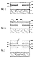
- Figure 1 shows a copper line 1 flush with one side 2 of a deposited dielectric 3 on a semiconductor substrate.
- interface layer 4 serving as a barrier layer to the diffusion of copper.
- Layer 4 has a thickness between 10 and 30 nm.
- a layer 5 of dielectric material with low permittivity is deposited on layer 4. Its thickness is between 0.5 and 1 ⁇ m.
- FIG. 3 shows that a layer interface 10 has been deposited on the material layer dielectric 5.
- the interface layer 10, intended for constitute a hard mask includes an underlay 11 made of SiCH deposited on the layer of dielectric material 5 and an undercoat 12 of SiOCH deposited on the undercoat 11.
- the underlay 11 may have a thickness between 10 and 20 nm while the thickness of the sublayer 12 is of the order of 100 nm. This stacking of undercoats is compatible with the material to be low permittivity of layer 5 because SiCH does not oxidize the dielectric and ensures excellent etching selectivity: hard / dielectric mask low permittivity.
- a layer of photosensitive resin 20 is deposited on the layer interface or hard mask 10 and an engraving hole 21 y is defined opposite line 1.
- the etching of the hard mask 10 is done in three operations. A hole is first etched in the sub-layer 12 in SiOCH until the sub-layer 11 in SiCH is revealed. The resin layer 20 is then removed, the dielectric layer via 5, which is very sensitive to the oxidation produced by the oxidizing agents for removing the resin (plasma O 2 , organic bases, etc.), being then protected by the sublayer 11 as shown in FIG. 4. Finally, the sublayer 11 is etched using the sublayer 12 as a mask, the sublayer 12 being partially etched.
- a layer 6 of dielectric material with low permittivity called “line dielectric” is deposited on the layer interface 10 and fills the hole made on the layer interface 10.
- the thickness of layer 6 can be between 0.3 and 0.6 ⁇ m.
- the interface layer 30 is then deposited on the layer of dielectric material 6 like the shows Figure 6.
- the interface layer 30 includes three sublayers: in the order of deposition one sublayer 31 in SiCH of thickness less than 10 nm and compatible with the dielectric material of the layer 6, a SiOCH sublayer 32 with a thickness comprised between 100 and 150 nm and a 33 SiCH sublayer slightly greater than the sum of the thicknesses of layer 2 and sublayer 31 in SiCH.
- the interface layer 30 will serve as a layer stop chemical mechanical polishing and also mask hard.
- the underlay 31 is used in particular to avoid oxidation of the dielectric layer 6.
- the undercoat 32 serves as a stop layer for polishing. She protects the dielectric layer 6 from faults of polishing uniformities. It limits the effect of copper removal during the chemical mechanical polishing.
- the underlay 33 serves as engraving counter mask allowing to engrave in one single step a hole revealing line 1.
- a layer of photosensitive resin 40 is deposited on the layer interface 30 and an etching hole 41 is defined therein opposite the hole previously etched in the hard mask 10.
- a hole is first engraved in the underlay 33 in SiCH with stop in sublayer 32 in SiOCH. The resin is then removed, the dielectric material of layer 6 being protected by sublayers 31 and 32.
- the engraving of the hard mask 30 is continued until the layer is revealed line 6 dielectric.
- the SiCH underlay 33 is engraved over its entire surface at least one thickness equivalent to the thickness of the SiCH sublayer 31.
- FIG 10 shows the presence of a copper connection 9 passing through the dielectric layer via 5 and the layer of dielectric line 6 to contact the line 1.
- layer 6 line dielectric
- dielectric constant equivalent to this stack is 2.25.
- the use of SiN in place of SiCH and the use of SiO 2 in place of SiOCH would lead to an equivalent dielectric constant of 2.55.
Landscapes
- Internal Circuitry In Semiconductor Integrated Circuit Devices (AREA)
Abstract
Description
- Les matériaux à usage de barrière doivent posséder une bonne résistance à la diffusion du cuivre.
- Les matériaux à usage de masque dur doivent présenter une excellente sélectivité de gravure vis-à-vis des matériaux sous-jacents de type organique ou minéral.
- Les matériaux à usage de couche d'arrêt au polissage doivent présenter une bonne résistance au polissage mécano-chimique afin de permettre l'élimination du cuivre excédentaire au-dessus des lignes sans qu'il y ait dégradation du diélectrique. Autrement dit, ces matériaux doivent présenter une sélectivité au polissage élevée vis-à-vis du cuivre.
- Tous ces matériaux doivent de plus avoir de bonnes tenues électriques : faible constante diélectrique, faible courant de fuite.
- Les matériaux déposés directement sur les diélectriques à très faible permittivité (matériaux des masques durs et des couches d'arrêt) doivent présenter une bonne compatibilité chimique avec ces diélectriques.
- dépôt sur ladite face à connecter d'une couche barrière à la diffusion du cuivre en SiCH,
- dépôt sur la couche barrière d'une première couche de matériau diélectrique de très faible permittivité pour le logement desdites interconnexions,
- dépôt d'une première couche d'interface sur ladite première couche de matériau diélectrique, comprenant une sous-couche de SiCH, déposée sur et en contact avec la première couche de matériau diélectrique, et une sous-couche de SiOCH,
- gravure de trous dans ladite sous-couche de SiOCH, en vis-à-vis des lignes conductrices à connecter, au moyen d'un masque de résine, jusqu'à révéler la sous-couche de SiCH,
- retrait du masque de résine,
- gravure de la partie de la sous-couche de SiCH révélée jusqu'à atteindre la première couche de matériau diélectrique,
- dépôt sur la première couche d'interface gravée d'une deuxième couche de matériau diélectrique de très faible permittivité pour le logement desdites interconnexions,
- dépôt d'une deuxième couche d'interface sur ladite deuxième couche de matériau diélectrique, comprenant successivement une première sous-couche de SiCH, déposée sur et en contact avec la deuxième couche de matériau diélectrique, une deuxième sous-couche de SiOCH et une troisième sous-couche de SiCH,
- gravure de trous dans ladite troisième sous-couche, en vis-à-vis des lignes conductrices à connecter, au moyen d'un masque de résine, jusqu'à révéler la deuxième sous-couche,
- retrait du masque de résine,
- gravure de la partie de la deuxième sous-couche révélée et de la partie de la première sous-couche révélée par la gravure de la deuxième sous-couche,
- gravure de trous au travers de la deuxième couche de matériau diélectrique, de la première couche de matériau diélectrique et de la couche barrière, lesdites couches d'interface servant de masque dur, jusqu'à révéler les lignes conductrices, ladite troisième sous-couche étant également éliminée,
- dépôt uniforme d'une couche métallique servant de barrière à la diffusion du cuivre sur l'empilement de couches gravées,
- dépôt d'une couche de cuivre remplissant les trous gravés dans la structure,
- polissage de l'excès de cuivre et de la couche métallique recouvrant la deuxième sous-couche pour révéler la deuxième sous-couche et fournir les interconnexions.
- une couche barrière à la diffusion du cuivre en SiCH déposée sur ladite face,
- une première couche de matériau diélectrique de très faible permittivité déposée sur la couche barrière,
- une première couche d'interface déposée sur ladite première couche de matériau diélectrique, comprenant une sous-couche de SiCH, déposée sur et en contact avec la première couche de matériau diélectrique, et une sous-couche de SiOCH,
- une deuxième couche de matériau diélectrique de très faible permittivité déposée sur la première couche d'interface,
- une deuxième couche d'interface déposée sur ladite deuxième couche de matériau diélectrique, comprenant une première sous-couche de SiCH, déposée sur et en contact avec la deuxième couche de matériau diélectrique, et une deuxième sous-couche de SiOCH,
- des interconnexions en cuivre traversant ladite structure pour établir des liaisons électriques avec lesdites lignes conductrices, une couche barrière à la diffusion du cuivre séparant les interconnexions des couches de matériau diélectrique de très faible permittivité.
| Propriétés | Matériaux | ||||
| SiO2 | Si3N4 | SiON | SiCH | SiOCH | |
| Constante Diélectrique | 4,3 | 8 | 6,5 | 5,5 | 2,7 |
| Sélectivité gravure fluorée/SiO2 | 0 | ++ | + | +++ | + |
| Résistance à l'abrasion/Cu | + | ++ | + | +++ | ++ |
| Diffusion Cu | - | ++ | - | +++ | - |
| Compatibilité chimique | --- | + | - | + | -- |
Claims (13)
- Procédé de réalisation d'une structure d'interconnexions de type Damascène sur une face (2) à connecter d'un dispositif micro-électronique, le procédé comprenant le dépôt d'au moins une couche de matériau diélectrique (5, 6) sur ladite face (2) à connecter, destinée à loger lesdites interconnexions (9), le procédé comprenant également le dépôt d'au moins une couche d'interface (10, 30) en matériau diélectrique en contact intime avec ladite couche de matériau diélectrique (5, 6) destinée à loger les interconnexions (9), caractérisé en ce que ladite couche d'interface (10, 30) est formée par le dépôt d'au moins une sous-couche (12, 32) de SiOCH et d'au moins une sous-couche de SiCH (11, 31, 33).
- Procédé selon la revendication 1, caractérisé en ce que le dépôt d'une couche de matériau diélectrique (5, 6) destinée à loger les interconnexions (9) consiste à déposer une couche d'un matériau choisi parmi les matériaux diélectriques à très faible permittivité de type minéral à base Si-O, comportant des radicaux organiques ou hydrures.
- Procédé selon l'une des revendications 1 ou 2, caractérisé en ce que la couche d'interface (10, 30) comprend une sous-couche en SiCH (11, 31) déposée sur et en contact avec la couche de matériau diélectrique (5, 6) destinée à loger les interconnexions (9), une sous-couche en SiOCH (12, 32) étant déposée sur et en contact avec la sous-couche en SiCH (11, 31).
- Procédé selon l'une quelconque des revendications 1 à 3, caractérisé en ce que le dispositif micro-électronique est réalisé sur du silicium (3).
- Procédé selon l'une quelconque des revendications 1 à 4, caractérisé en ce que les interconnexions (9) étant en cuivre, il est prévu le dépôt d'une couche métallique (8) formant barrière à la diffusion du cuivre dans la couche de matériau diélectrique (5, 6) destinée à loger les interconnexions.
- Procédé selon la revendication 3, caractérisé en ce que la sous-couche de SiOCH (12) est utilisée comme masque de gravure pour la sous-couche de SiCH (11) en vue de loger les interconnexions (9) dans la couche de matériau diélectrique correspondante.
- Procédé de réalisation d'une structure d'interconnexions de type double Damascène sur une face (2) à connecter d'un dispositif micro-électronique réalisé sur du silicium, ladite face (2) présentant des lignes conductrices en cuivre (1) à connecter, caractérisé en ce qu'il comprend les étapes suivantes :dépôt sur ladite face (2) à connecter d'une couche barrière à la diffusion du cuivre (4) en SiCH,dépôt sur la couche barrière (4) d'une première couche de matériau diélectrique de très faible permittivité (5) pour le logement desdites interconnexions,dépôt d'une première couche d'interface (10) sur ladite première couche de matériau diélectrique (5), comprenant une sous-couche (11) de SiCH, déposée sur et en contact avec la première couche de matériau diélectrique, et une sous-couche (12) de SiOCH,gravure de trous dans ladite sous-couche (12) de SiOCH, en vis-à-vis des lignes conductrices (1) à connecter, au moyen d'un masque de résine (20), jusqu'à révéler la sous-couche (11) de SiCH,retrait du masque de résine (20),gravure de la partie de la sous-couche (11) de SiCH révélée jusqu'à atteindre la première couche de matériau diélectrique (5),dépôt sur la première couche d'interface (10) gravée d'une deuxième couche de matériau diélectrique de très faible permittivité (6) pour le logement desdites interconnexions,dépôt d'une deuxième couche d'interface (30) sur ladite deuxième couche de matériau diélectrique (6), comprenant successivement une première sous-couche (31) de SiCH, déposée sur et en contact avec la deuxième couche de matériau diélectrique (6), une deuxième sous-couche (32) de SiOCH et une troisième sous-couche (33) de SiCH,gravure de trous dans ladite troisième sous-couche (33), en vis-à-vis des lignes conductrices (1) à connecter, au moyen d'un masque de résine (40), jusqu'à révéler la deuxième sous-couche (32),retrait du masque de résine (40),gravure de la partie de la deuxième sous-couche (32) révélée et de la partie de la première sous-couche (31) révélée par la gravure de la deuxième sous-couche (32),gravure de trous (7) au travers de la deuxième couche de matériau diélectrique (6), de la première couche de matériau diélectrique (5) et de la couche barrière (4), lesdites couches d'interface (30, 10) servant de masque dur, jusqu'à révéler les lignes conductrices (1), ladite troisième sous-couche (33) étant également éliminée,dépôt uniforme d'une couche métallique (8) servant de barrière à la diffusion du cuivre sur l'empilement de couches gravées,dépôt d'une couche de cuivre remplissant les trous (7) gravés dans la structure,polissage de l'excès de cuivre et de la couche métallique (8) recouvrant la deuxième sous-couche (32) pour révéler la deuxième sous-couche (32) et fournir les interconnexions (9).
- Structure d'interconnexions de type Damascène sur une face d'un dispositif micro-électronique, comprenant au moins une couche de matériau diélectrique (5, 6) destinée à loger lesdites interconnexions (9) et comprenant au moins une couche d'interface (10) en matériau diélectrique en contact intime avec ladite couche de matériau diélectrique destinée à loger les interconnexions, caractérisée en ce que ladite couche d'interface (10) comprend au moins une sous-couche de SiOCH (12) et au moins une sous-couche de SiCH (11).
- Structure d'interconnexions selon la revendication 8, caractérisée en ce que la couche de matériau diélectrique (5, 6) destinée à loger lesdites interconnexions (9) est une couche d'un matériau choisi parmi les matériaux diélectriques à très faible permittivité de type minéral à base Si-O, comportant des radicaux organiques ou hydrures.
- Structure d'interconnexions selon l'une des revendications 8 ou 9, caractérisée en ce que la couche d'interface (10) comprend une sous-couche (11) en SiCH sur et en contact avec la couche de matériau diélectrique (5) destinée à loger les interconnexions, une sous-couche (12) en SiOCH étant disposée sur et en contact avec la sous-couche (11) en SiCH.
- Structure d'interconnexions selon l'une quelconque des revendications 8 à 10, caractérisée en ce que le dispositif micro-électronique est un dispositif réalisé sur du silicium (3).
- Structure d'interconnexions selon l'une quelconque des revendications 8 à 11, caractérisée en ce que les interconnexions (9) étant en cuivre, la structure comprend une couche métallique (8) formant barrière à la diffusion du cuivre dans la couche de matériau diélectrique (5, 6) destinée à loger les interconnexions (9).
- Structure d'interconnexions de type double Damascène sur une face (2) à connecter d'un dispositif micro-électronique réalisé sur du silicium, ladite face (2) présentant des lignes conductrices (1) en cuivre à connecter, caractérisée en ce qu'elle comprend :une couche barrière à la diffusion du cuivre (4) en SiCH déposée sur ladite face (2),une première couche de matériau diélectrique de très faible permittivité (5) déposée sur la couche barrière (4),une première couche d'interface (10) déposée sur ladite première couche de matériau diélectrique (5), comprenant une sous-couche (11) de SiCH, déposée sur et en contact avec la première couche de matériau diélectrique (5), et une sous-couche (12) de SiOCH,une deuxième couche de matériau diélectrique de très faible permittivité (6) déposée sur la première couche d'interface (10),une deuxième couche d'interface (30) déposée sur ladite deuxième couche de matériau diélectrique (6), comprenant une première sous-couche (31) de SiCH, déposée sur et en contact avec la deuxième couche de matériau diélectrique (6), et une deuxième sous-couche (32) de SiOCH,des interconnexions (9) en cuivre traversant ladite structure pour établir des liaisons électriques avec lesdites lignes conductrices (1), une couche barrière à la diffusion du cuivre (8) séparant les interconnexions (9) des couches de matériau diélectrique de très faible permittivité (5, 6).
Applications Claiming Priority (2)
| Application Number | Priority Date | Filing Date | Title |
|---|---|---|---|
| FR9915669A FR2802336B1 (fr) | 1999-12-13 | 1999-12-13 | Structure d'interconnexions de type damascene et son procede de realisation |
| FR9915669 | 1999-12-13 |
Publications (3)
| Publication Number | Publication Date |
|---|---|
| EP1109221A2 true EP1109221A2 (fr) | 2001-06-20 |
| EP1109221A3 EP1109221A3 (fr) | 2001-09-12 |
| EP1109221B1 EP1109221B1 (fr) | 2006-11-02 |
Family
ID=9553165
Family Applications (1)
| Application Number | Title | Priority Date | Filing Date |
|---|---|---|---|
| EP00403464A Expired - Lifetime EP1109221B1 (fr) | 1999-12-13 | 2000-12-11 | Structure d'interconnexions de type damascène et son procédé de réalisation |
Country Status (4)
| Country | Link |
|---|---|
| US (1) | US6624053B2 (fr) |
| EP (1) | EP1109221B1 (fr) |
| DE (1) | DE60031637D1 (fr) |
| FR (1) | FR2802336B1 (fr) |
Cited By (1)
| Publication number | Priority date | Publication date | Assignee | Title |
|---|---|---|---|---|
| EP3098851A2 (fr) | 2015-05-28 | 2016-11-30 | Commissariat A L'energie Atomique Et Aux Energies Alternatives | Procédé de réalisation d'un filtre infrarouge associé à un capteur d'image |
Families Citing this family (41)
| Publication number | Priority date | Publication date | Assignee | Title |
|---|---|---|---|---|
| US20020086547A1 (en) * | 2000-02-17 | 2002-07-04 | Applied Materials, Inc. | Etch pattern definition using a CVD organic layer as an anti-reflection coating and hardmask |
| TW535253B (en) * | 2000-09-08 | 2003-06-01 | Applied Materials Inc | Plasma treatment of silicon carbide films |
| US6979903B1 (en) * | 2001-06-04 | 2005-12-27 | Advanced Micro Devices, Inc. | Integrated circuit with dielectric diffusion barrier layer formed between interconnects and interlayer dielectric layers |
| US6469385B1 (en) * | 2001-06-04 | 2002-10-22 | Advanced Micro Devices, Inc. | Integrated circuit with dielectric diffusion barrier layer formed between interconnects and interlayer dielectric layers |
| KR100668819B1 (ko) * | 2001-06-26 | 2007-01-17 | 주식회사 하이닉스반도체 | 반도체 소자의 제조 방법 |
| US6879046B2 (en) * | 2001-06-28 | 2005-04-12 | Agere Systems Inc. | Split barrier layer including nitrogen-containing portion and oxygen-containing portion |
| US7642202B1 (en) | 2001-06-28 | 2010-01-05 | Novellus Systems, Inc. | Methods of forming moisture barrier for low k film integration with anti-reflective layers |
| US6797605B2 (en) * | 2001-07-26 | 2004-09-28 | Chartered Semiconductor Manufacturing Ltd. | Method to improve adhesion of dielectric films in damascene interconnects |
| US20030064582A1 (en) * | 2001-09-28 | 2003-04-03 | Oladeji Isaiah O. | Mask layer and interconnect structure for dual damascene semiconductor manufacturing |
| JP2003124189A (ja) * | 2001-10-10 | 2003-04-25 | Fujitsu Ltd | 半導体装置の製造方法 |
| US6838393B2 (en) | 2001-12-14 | 2005-01-04 | Applied Materials, Inc. | Method for producing semiconductor including forming a layer containing at least silicon carbide and forming a second layer containing at least silicon oxygen carbide |
| US7091137B2 (en) * | 2001-12-14 | 2006-08-15 | Applied Materials | Bi-layer approach for a hermetic low dielectric constant layer for barrier applications |
| US6890850B2 (en) | 2001-12-14 | 2005-05-10 | Applied Materials, Inc. | Method of depositing dielectric materials in damascene applications |
| KR100799118B1 (ko) * | 2001-12-19 | 2008-01-29 | 주식회사 하이닉스반도체 | 다층 구리 배선의 형성 방법 |
| US20030119305A1 (en) * | 2001-12-21 | 2003-06-26 | Huang Robert Y. S. | Mask layer and dual damascene interconnect structure in a semiconductor device |
| US6911389B2 (en) * | 2002-09-18 | 2005-06-28 | Texas Instruments Incorporated | Self aligned vias in dual damascene interconnect, buried mask approach |
| US7749563B2 (en) * | 2002-10-07 | 2010-07-06 | Applied Materials, Inc. | Two-layer film for next generation damascene barrier application with good oxidation resistance |
| GB2394879B (en) | 2002-11-04 | 2005-11-23 | Electrolux Outdoor Prod Ltd | Trimmer |
| US6917108B2 (en) * | 2002-11-14 | 2005-07-12 | International Business Machines Corporation | Reliable low-k interconnect structure with hybrid dielectric |
| US6706629B1 (en) * | 2003-01-07 | 2004-03-16 | Taiwan Semiconductor Manufacturing Company | Barrier-free copper interconnect |
| JP3898133B2 (ja) * | 2003-01-14 | 2007-03-28 | Necエレクトロニクス株式会社 | SiCHN膜の成膜方法。 |
| JP4068072B2 (ja) * | 2003-01-29 | 2008-03-26 | Necエレクトロニクス株式会社 | 半導体装置及びその製造方法 |
| US6913992B2 (en) | 2003-03-07 | 2005-07-05 | Applied Materials, Inc. | Method of modifying interlayer adhesion |
| US7071539B2 (en) * | 2003-07-28 | 2006-07-04 | International Business Machines Corporation | Chemical planarization performance for copper/low-k interconnect structures |
| US20050077629A1 (en) * | 2003-10-14 | 2005-04-14 | International Business Machines Corporation | Photoresist ash process with reduced inter-level dielectric ( ILD) damage |
| US7030041B2 (en) | 2004-03-15 | 2006-04-18 | Applied Materials Inc. | Adhesion improvement for low k dielectrics |
| US7229911B2 (en) | 2004-04-19 | 2007-06-12 | Applied Materials, Inc. | Adhesion improvement for low k dielectrics to conductive materials |
| US7288205B2 (en) | 2004-07-09 | 2007-10-30 | Applied Materials, Inc. | Hermetic low dielectric constant layer for barrier applications |
| US7265437B2 (en) * | 2005-03-08 | 2007-09-04 | International Business Machines Corporation | Low k dielectric CVD film formation process with in-situ imbedded nanolayers to improve mechanical properties |
| JP2007053220A (ja) * | 2005-08-18 | 2007-03-01 | Oki Electric Ind Co Ltd | 半導体装置の製造方法 |
| JP4231055B2 (ja) * | 2006-02-06 | 2009-02-25 | 株式会社東芝 | 半導体装置及びその製造方法 |
| US8084862B2 (en) * | 2007-09-20 | 2011-12-27 | International Business Machines Corporation | Interconnect structures with patternable low-k dielectrics and method of fabricating same |
| US8618663B2 (en) | 2007-09-20 | 2013-12-31 | International Business Machines Corporation | Patternable dielectric film structure with improved lithography and method of fabricating same |
| US7709370B2 (en) | 2007-09-20 | 2010-05-04 | International Business Machines Corporation | Spin-on antireflective coating for integration of patternable dielectric materials and interconnect structures |
| JP2010003894A (ja) * | 2008-06-20 | 2010-01-07 | Nec Electronics Corp | 半導体装置の製造方法及び半導体装置 |
| US8138093B2 (en) * | 2009-08-12 | 2012-03-20 | International Business Machines Corporation | Method for forming trenches having different widths and the same depth |
| JP5404365B2 (ja) * | 2009-12-16 | 2014-01-29 | キヤノン株式会社 | 電気機械変換装置及びその製造方法 |
| CN104465491B (zh) * | 2013-09-23 | 2018-01-12 | 中芯国际集成电路制造(上海)有限公司 | 金属互连层的形成方法 |
| US10380868B2 (en) * | 2016-08-25 | 2019-08-13 | Infineon Technologies Ag | Sensor devices |
| US10872861B2 (en) * | 2018-02-07 | 2020-12-22 | Advanced Semiconductor Engineering, Inc. Kaohsiung, Taiwan | Semiconductor packages |
| US20240379561A1 (en) * | 2023-05-09 | 2024-11-14 | Nanya Technology Corporation | Interconnect structure and manufacturing method thereof |
Family Cites Families (4)
| Publication number | Priority date | Publication date | Assignee | Title |
|---|---|---|---|---|
| US6159871A (en) * | 1998-05-29 | 2000-12-12 | Dow Corning Corporation | Method for producing hydrogenated silicon oxycarbide films having low dielectric constant |
| US6331479B1 (en) * | 1999-09-20 | 2001-12-18 | Chartered Semiconductor Manufacturing Ltd. | Method to prevent degradation of low dielectric constant material in copper damascene interconnects |
| US6372661B1 (en) * | 2000-07-14 | 2002-04-16 | Taiwan Semiconductor Manufacturing Company | Method to improve the crack resistance of CVD low-k dielectric constant material |
| US6350675B1 (en) * | 2000-10-12 | 2002-02-26 | Chartered Semiconductor Manufacturing Ltd. | Integration of silicon-rich material in the self-aligned via approach of dual damascene interconnects |
-
1999
- 1999-12-13 FR FR9915669A patent/FR2802336B1/fr not_active Expired - Fee Related
-
2000
- 2000-12-06 US US09/731,090 patent/US6624053B2/en not_active Expired - Lifetime
- 2000-12-11 DE DE60031637T patent/DE60031637D1/de not_active Expired - Lifetime
- 2000-12-11 EP EP00403464A patent/EP1109221B1/fr not_active Expired - Lifetime
Cited By (1)
| Publication number | Priority date | Publication date | Assignee | Title |
|---|---|---|---|---|
| EP3098851A2 (fr) | 2015-05-28 | 2016-11-30 | Commissariat A L'energie Atomique Et Aux Energies Alternatives | Procédé de réalisation d'un filtre infrarouge associé à un capteur d'image |
Also Published As
| Publication number | Publication date |
|---|---|
| FR2802336A1 (fr) | 2001-06-15 |
| US20010004550A1 (en) | 2001-06-21 |
| DE60031637D1 (de) | 2006-12-14 |
| US6624053B2 (en) | 2003-09-23 |
| EP1109221B1 (fr) | 2006-11-02 |
| EP1109221A3 (fr) | 2001-09-12 |
| FR2802336B1 (fr) | 2002-03-01 |
Similar Documents
| Publication | Publication Date | Title |
|---|---|---|
| EP1109221B1 (fr) | Structure d'interconnexions de type damascène et son procédé de réalisation | |
| US6245665B1 (en) | Semiconductor device and method of fabricating the same | |
| KR0160338B1 (ko) | 반도체 장치의 제조 방법 | |
| US7816280B2 (en) | Semiconductor device, semiconductor wafer, and methods of producing the same device and wafer | |
| KR100288827B1 (ko) | 반도체장치 및 그 제조방법 | |
| US7088003B2 (en) | Structures and methods for integration of ultralow-k dielectrics with improved reliability | |
| US7265038B2 (en) | Method for forming a multi-layer seed layer for improved Cu ECP | |
| KR100689917B1 (ko) | 반도체 장치 및 그 제조 방법 | |
| US7951705B2 (en) | Multilayered cap barrier in microelectronic interconnect structures | |
| CN100461352C (zh) | 互连结构及其形成方法 | |
| US7705431B1 (en) | Method of improving adhesion between two dielectric films | |
| JP3211950B2 (ja) | 半導体装置およびその製造方法 | |
| US20060024954A1 (en) | Copper damascene barrier and capping layer | |
| US7642185B2 (en) | Insulating film forming method capable of enhancing adhesion of silicon carbide film, etc. and semiconductor device | |
| JPH1140671A (ja) | 半導体装置を形成するためのプロセス | |
| US20040041269A1 (en) | Semiconductor device and manufacturing method thereof | |
| EP1243024B1 (fr) | Procede de formation d'une structure d'interconnexions dont l'isolant inclut des cavites | |
| KR100541185B1 (ko) | 캡핑막을 포함하는 층간절연막 및 이를 포함하는 금속배선형성 방법 | |
| FR2798512A1 (fr) | Procede de realisation d'une connexion en cuivre au travers d'une couche de materiau dielectrique d'un circuit integre | |
| US6184120B1 (en) | Method of forming a buried plug and an interconnection | |
| US6867135B1 (en) | Via bottom copper/barrier interface improvement to resolve via electromigration and stress migration | |
| CA2006174A1 (fr) | Methode de fabrication de films isolants sans craquelures au moyen de couches intermediaires de verre de spin | |
| JP3159134B2 (ja) | 半導体集積回路装置 | |
| JPH11111845A (ja) | 半導体装置及びその製造方法 | |
| JP4108189B2 (ja) | 配線構造、及びその形成方法 |
Legal Events
| Date | Code | Title | Description |
|---|---|---|---|
| PUAI | Public reference made under article 153(3) epc to a published international application that has entered the european phase |
Free format text: ORIGINAL CODE: 0009012 |
|
| AK | Designated contracting states |
Kind code of ref document: A2 Designated state(s): AT BE CH CY DE DK ES FI FR GB GR IE IT LI LU MC NL PT SE TR Kind code of ref document: A2 Designated state(s): DE FR GB IT |
|
| AX | Request for extension of the european patent |
Free format text: AL;LT;LV;MK;RO;SI |
|
| PUAL | Search report despatched |
Free format text: ORIGINAL CODE: 0009013 |
|
| AK | Designated contracting states |
Kind code of ref document: A3 Designated state(s): AT BE CH CY DE DK ES FI FR GB GR IE IT LI LU MC NL PT SE TR |
|
| AX | Request for extension of the european patent |
Free format text: AL;LT;LV;MK;RO;SI |
|
| RAP1 | Party data changed (applicant data changed or rights of an application transferred) |
Owner name: STMICROELECTRONICS S.A. |
|
| 17P | Request for examination filed |
Effective date: 20020215 |
|
| AKX | Designation fees paid |
Free format text: DE FR GB IT |
|
| GRAP | Despatch of communication of intention to grant a patent |
Free format text: ORIGINAL CODE: EPIDOSNIGR1 |
|
| GRAS | Grant fee paid |
Free format text: ORIGINAL CODE: EPIDOSNIGR3 |
|
| GRAA | (expected) grant |
Free format text: ORIGINAL CODE: 0009210 |
|
| AK | Designated contracting states |
Kind code of ref document: B1 Designated state(s): DE FR GB IT |
|
| PG25 | Lapsed in a contracting state [announced via postgrant information from national office to epo] |
Ref country code: IT Free format text: LAPSE BECAUSE OF FAILURE TO SUBMIT A TRANSLATION OF THE DESCRIPTION OR TO PAY THE FEE WITHIN THE PRE;WARNING: LAPSES OF ITALIAN PATENTS WITH EFFECTIVE DATE BEFORE 2007 MAY HAVE OCCURRED AT ANY TIME BEFORE 2007. THE CORRECT EFFECTIVE DATE MAY BE DIFFERENT FROM THE ONE RECORDED.SCRIBED TIME-LIMIT Effective date: 20061102 |
|
| REG | Reference to a national code |
Ref country code: GB Ref legal event code: FG4D Free format text: NOT ENGLISH |
|
| REF | Corresponds to: |
Ref document number: 60031637 Country of ref document: DE Date of ref document: 20061214 Kind code of ref document: P |
|
| PG25 | Lapsed in a contracting state [announced via postgrant information from national office to epo] |
Ref country code: DE Free format text: LAPSE BECAUSE OF FAILURE TO SUBMIT A TRANSLATION OF THE DESCRIPTION OR TO PAY THE FEE WITHIN THE PRESCRIBED TIME-LIMIT Effective date: 20070203 |
|
| GBT | Gb: translation of ep patent filed (gb section 77(6)(a)/1977) |
Effective date: 20070111 |
|
| PLBE | No opposition filed within time limit |
Free format text: ORIGINAL CODE: 0009261 |
|
| STAA | Information on the status of an ep patent application or granted ep patent |
Free format text: STATUS: NO OPPOSITION FILED WITHIN TIME LIMIT |
|
| 26N | No opposition filed |
Effective date: 20070803 |
|
| PGFP | Annual fee paid to national office [announced via postgrant information from national office to epo] |
Ref country code: GB Payment date: 20101201 Year of fee payment: 11 |
|
| PGFP | Annual fee paid to national office [announced via postgrant information from national office to epo] |
Ref country code: FR Payment date: 20110120 Year of fee payment: 11 |
|
| GBPC | Gb: european patent ceased through non-payment of renewal fee |
Effective date: 20111211 |
|
| REG | Reference to a national code |
Ref country code: FR Ref legal event code: ST Effective date: 20120831 |
|
| PG25 | Lapsed in a contracting state [announced via postgrant information from national office to epo] |
Ref country code: GB Free format text: LAPSE BECAUSE OF NON-PAYMENT OF DUE FEES Effective date: 20111211 |
|
| PG25 | Lapsed in a contracting state [announced via postgrant information from national office to epo] |
Ref country code: FR Free format text: LAPSE BECAUSE OF NON-PAYMENT OF DUE FEES Effective date: 20120102 |