EP1111903A1 - Dispositif et procédé d'écriture optique - Google Patents
Dispositif et procédé d'écriture optique Download PDFInfo
- Publication number
- EP1111903A1 EP1111903A1 EP00125345A EP00125345A EP1111903A1 EP 1111903 A1 EP1111903 A1 EP 1111903A1 EP 00125345 A EP00125345 A EP 00125345A EP 00125345 A EP00125345 A EP 00125345A EP 1111903 A1 EP1111903 A1 EP 1111903A1
- Authority
- EP
- European Patent Office
- Prior art keywords
- light
- semiconductor laser
- over
- outputting
- change
- Prior art date
- Legal status (The legal status is an assumption and is not a legal conclusion. Google has not performed a legal analysis and makes no representation as to the accuracy of the status listed.)
- Granted
Links
Images


Classifications
-
- H—ELECTRICITY
- H04—ELECTRIC COMMUNICATION TECHNIQUE
- H04N—PICTORIAL COMMUNICATION, e.g. TELEVISION
- H04N1/00—Scanning, transmission or reproduction of documents or the like, e.g. facsimile transmission; Details thereof
- H04N1/40—Picture signal circuits
- H04N1/40025—Circuits exciting or modulating particular heads for reproducing continuous tone value scales
- H04N1/4005—Circuits exciting or modulating particular heads for reproducing continuous tone value scales with regulating circuits, e.g. dependent upon ambient temperature or feedback control
-
- G—PHYSICS
- G06—COMPUTING OR CALCULATING; COUNTING
- G06K—GRAPHICAL DATA READING; PRESENTATION OF DATA; RECORD CARRIERS; HANDLING RECORD CARRIERS
- G06K15/00—Arrangements for producing a permanent visual presentation of the output data, e.g. computer output printers
- G06K15/02—Arrangements for producing a permanent visual presentation of the output data, e.g. computer output printers using printers
- G06K15/12—Arrangements for producing a permanent visual presentation of the output data, e.g. computer output printers using printers by photographic printing, e.g. by laser printers
- G06K15/1204—Arrangements for producing a permanent visual presentation of the output data, e.g. computer output printers using printers by photographic printing, e.g. by laser printers involving the fast moving of an optical beam in the main scanning direction
- G06K15/1219—Detection, control or error compensation of scanning velocity or position, e.g. synchronisation
-
- G—PHYSICS
- G06—COMPUTING OR CALCULATING; COUNTING
- G06K—GRAPHICAL DATA READING; PRESENTATION OF DATA; RECORD CARRIERS; HANDLING RECORD CARRIERS
- G06K15/00—Arrangements for producing a permanent visual presentation of the output data, e.g. computer output printers
- G06K15/02—Arrangements for producing a permanent visual presentation of the output data, e.g. computer output printers using printers
- G06K15/12—Arrangements for producing a permanent visual presentation of the output data, e.g. computer output printers using printers by photographic printing, e.g. by laser printers
- G06K15/1238—Arrangements for producing a permanent visual presentation of the output data, e.g. computer output printers using printers by photographic printing, e.g. by laser printers simultaneously exposing more than one point
- G06K15/1257—Arrangements for producing a permanent visual presentation of the output data, e.g. computer output printers using printers by photographic printing, e.g. by laser printers simultaneously exposing more than one point on more than one main scanning line
- G06K15/1261—Arrangements for producing a permanent visual presentation of the output data, e.g. computer output printers using printers by photographic printing, e.g. by laser printers simultaneously exposing more than one point on more than one main scanning line using an array of light sources
-
- H—ELECTRICITY
- H01—ELECTRIC ELEMENTS
- H01S—DEVICES USING THE PROCESS OF LIGHT AMPLIFICATION BY STIMULATED EMISSION OF RADIATION [LASER] TO AMPLIFY OR GENERATE LIGHT; DEVICES USING STIMULATED EMISSION OF ELECTROMAGNETIC RADIATION IN WAVE RANGES OTHER THAN OPTICAL
- H01S5/00—Semiconductor lasers
- H01S5/06—Arrangements for controlling the laser output parameters, e.g. by operating on the active medium
- H01S5/068—Stabilisation of laser output parameters
- H01S5/0683—Stabilisation of laser output parameters by monitoring the optical output parameters
-
- H—ELECTRICITY
- H04—ELECTRIC COMMUNICATION TECHNIQUE
- H04N—PICTORIAL COMMUNICATION, e.g. TELEVISION
- H04N1/00—Scanning, transmission or reproduction of documents or the like, e.g. facsimile transmission; Details thereof
- H04N1/40—Picture signal circuits
- H04N1/401—Compensating positionally unequal response of the pick-up or reproducing head
- H04N1/4015—Compensating positionally unequal response of the pick-up or reproducing head of the reproducing head
-
- H—ELECTRICITY
- H01—ELECTRIC ELEMENTS
- H01S—DEVICES USING THE PROCESS OF LIGHT AMPLIFICATION BY STIMULATED EMISSION OF RADIATION [LASER] TO AMPLIFY OR GENERATE LIGHT; DEVICES USING STIMULATED EMISSION OF ELECTROMAGNETIC RADIATION IN WAVE RANGES OTHER THAN OPTICAL
- H01S5/00—Semiconductor lasers
- H01S5/40—Arrangement of two or more semiconductor lasers, not provided for in groups H01S5/02 - H01S5/30
- H01S5/4025—Array arrangements, e.g. constituted by discrete laser diodes or laser bar
Definitions
- an LD array semiconductor laser array
- LD array semiconductor laser array
- a primary object of the present invention is to provide an optical scanning apparatus improving the defects and troublesome matters of the background arts. Since the LD array takes (adopts) a peculiar structure, being composed of plural light-emitting elements and a single light-receiving element, there exists no LD drive controlling circuit exclusively used for the LD array. For this reason, when the LD array is employed, it is necessary to construct the control circuit in a discrete state.
- LD arrays of the cathode-common type are commonly used.
- the LD drive controlling circuit of the cathode-common type LD of 1 CH (LD driver for use in 1 CH)
- many ICs including the APC function block (circuit for performing the APC operation) have been proposed up to now.
- the second aspect of the invention relates to an optical writing apparatus comprising: a semiconductor laser array comprising plural light-emitting elements and a single light-receiving element; and plural semiconductor laser drive controlling devices, wherein the plural semiconductor laser drive controlling devices respectively comprise: a current controlling device controlling the normal-direction currents flowing through the respective plural light-emitting elements such that the light-receiving signals, which correspond to the light-emitting levels (light intensities) of the respective light-emitting elements outputted from the light-receiving element in the semiconductor laser array, and the light-emitting level designating signals respectively become equal to each other; said optical writing apparatus further comprising: a change-over switching device; and an outputting timing determination device; wherein the outputting timing determination device further comprises: an outputting stopping device stopping the outputting of the change-over signal to the change-over switching device, after finishing the control operation by use of the current controlling device in the semiconductor laser drive controlling device connected to the negative feedback loop formed by the changing-over operation of the change-over switching device among
- Fig. 2 is a block diagram illustrating an example of the main part structure of the digital copying machine, comprising an optical writing apparatus of the embodiment according to the present invention.
- the CPU 21 is a central processing unit for totally controlling the entire portion of the main control section 20 in accordance with a control program stored in ROM 22.
- Fig. 1 is a construction block diagram illustrating an example of the structure of the writing apparatus (writing unit) in the printer section relating to the present invention.
- the laser beam 5 immediately before scanning the surface of the photosensitive drum 43, pass through a light detector 44 (synchronization detecting signal generating device) composed of a light-receiving element such as a photodiode, mounted e.g. outside of the main scanning writing area (outside of the predetermined main scanning width), e.g. on the photosensitive drum 43, the light detector 44 detects the laser beams, and creates and outputs a synchronization detecting signal for performing the positioning operation in the main scanning direction (namely, prescribing the position of starting the writing operation in the main scanning direction).
- a part of the laser beams generated e.g. by means of a beam splitter, may also be focused on the light-receiving element.
- the GAVD 11 is the one for practicing the function of an outputting timing determining device according to the first through third aspect of the present invention. GAVD 11 also respectively determines the output timing of outputting four image signals (DATA signals) to the four LD drive controlling circuits 60 (semiconductor laser drive controlling devices) in the LD control section 12, the output timing of outputting the SW changing-over signal to the changing-over switch circuit 65, and the output timing of outputting the APC signal (control starting signal) to the APC controlling sections 62 of the respective LD drive controlling circuit 60.
- DATA signals image signals
- LD drive controlling circuits 60 semiconductor laser drive controlling devices
- APC signal control starting signal
- the respective LD drive controlling circuits 60 respectively comprise the LD drive section 61 and the APC controlling section 62.
- the LD drive sections 61 in the respective LD drive controlling circuits 60 simultaneously drive the respective light-emitting elements of the light-emitting section 51 in the LD array 13 in accordance with the image signal from the GAVD 11.
- the LD drive sections 61 in the respective LD drive controlling circuits 60 simultaneously cause the light-emitting elements to respectively emit a laser beam. In such a way, the light writing operation per each of the plural lines is performed at the same time on the surface of the photosensitive drum 43 and thereby the electrostatic latent image is formed.
- the laser beam emitted backward from the light-emitting element 51 is directed as the incident light to the light-receiving section composed of the light-receiving element such as a photodiode, etc.
- the light-receiving section 52 detects the light intensity (light-emitting level of the light-emitting element) of the laser beam thus directed as the incident light.
- the incident laser beam is the beam emitted in order from the respective light-emitting elements in the light-emitting section 51 at the time of the APC operation.
- the light-receiving section 51 also outputs the light-receiving signal corresponding thereto to the APC controlling section 62 of either one of the LD drive controlling circuits 60 through the changing-over switch device.
- the APC controlling section 62 signifies the APC controlling section in the LD drive controlling circuits 60 having the LD drive section 61 which causes the corresponding light-emitting element to emit the light at this time.
- the changing-over switch circuit 65 is constructed with four changing-over switches 66-69. Either one of the changing-over switches 66-69 is selectively turned on (ON state) by the switch changing-over signal from the GAVD 11. Thereby, it is possible to change over the construction of the negative feedback loop (optoelectronic negative feedback loop) of either one of the LD drive controlling circuits 60 for the light-receiving signal outputted from the light-receiving section 52 of the LD array 13.
- the APC controlling section 62 in the respective LD drive controlling circuits 60 controls the LD drive section 61 in accordance with the inputted light-receiving signal, and further controls the light-emitting level of the corresponding light-emitting element in the light-emitting sections 51 of the LD arrays 13 (or the intensity of light emitted by the corresponding light-emitting element) so as to make the light-emitting level constant. Namely, the APC operation is performed. In such an APC operation, the normal-direction current flowing through the light-emitting element is controlled so as to respectively equalize the light-receiving signals to be inputted (corresponding to the light-emitting elements) to the light-emitting level designating signal.
- the voltage of the drive power source of the corresponding light-emitting element in the LD array 13 is adjusted and held such that the light-emitting level becomes constant, namely, the corresponding light-receiving signal and the light-receiving level are respectively equalized.
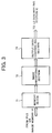
- Fig. 3 is a block diagram for illustrating the structural example of the GAVD 11.
- the GAVD 11 is provided with a memory block 71 for practicing the speed conversion and the format conversion for the data (image signal) from the IPU 3 or the image memory 24, an image processing section 72 for practicing the predetermined image processing for the data from the memory block 71, and an output data controlling section 73 for practicing the processes such as the conversion and the P sensor pattern applying, etc.
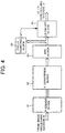
- Fig. 4 is a block diagram illustrating the structural example of the output data controlling section 73 as shown in Fig. 3.
- the output data controlling section 73 is provided with a P sensor block 81 for applying a P sensor pattern for putting the toner of a predetermined constant density on the photosensitive drum 43 for the purpose of acquiring the data for determining the processing condition to the data inputted from the image processing section 72, and ⁇ -conversion block 82 for causing the weight of the data to vary.
- the output data controlling section 73 is further provided with an APC block 83 for applying the image signal in synchronism with the APC operation timing in order to keep constant the light intensity (light amount) of the laser beam emitted from the respective light-emitting elements of the light-emitting section 51 in the LD array 13, a pixel count block 84 for counting the number of light-emitting dots (light-emitting pixels) emitted from the respective light-emitting sections 51 in the LD array 13, and an LD ON/OFF block 85 for applying the light-emitting data for the synchronization detecting output.
- an APC block 83 for applying the image signal in synchronism with the APC operation timing in order to keep constant the light intensity (light amount) of the laser beam emitted from the respective light-emitting elements of the light-emitting section 51 in the LD array 13
- a pixel count block 84 for counting the number of light-emitting dots (light-emitting pixels) emitted from the respective light-e
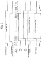
- Fig. 5 is a timing chart for illustrating an example of the operation of the printer section 10 relating to the present invention. Although Fig. 5 shows the APC operation during the time period of waiting, the timing of the APC operation does not change at all, even during the time period of printing (image formation). In this exemplary embodiment, the APC operation is performed for the 4 CH light-emitting elements (four-pieces LD) per one main scanning operation.
- the timing of outputting the above-mentioned respective signals by use of the GAVD 11 is cleared by the synchronization detecting signal employed in the GAVD 11.
- the same outputting timing is created by use of a not-shown main scanning counter, in which the counting-up operation is performed by the writing clock CLK.
- Those setting values can be changed at the time of setting the various setting data to a special (peculiar) mode capable of changing the setting data which is called the SP (Service-man Program) Mode, by use of the operation signal from the operation board section 30.
- SP Service-man Program
- the switch changing-over signals both for the image signal (DATA signal) and the APC signal.
- the GAVD 11 cannot create the switch changing-over signal because of the limitation of the pins number, etc.
- the APC signal and the switch changing-over signal can be newly created separately from the APC signal by providing a combination of plural digital circuits including two flip-flop circuits 91 and 92.
- Fig. 7 shows an example of the outputting timing of the respective signals in the GAVD 11 and the above-mentioned combination circuit.
- the embodiment according to the present invention may be applied to the optical writing apparatus (employing an LD array) of a digital copying machine.
- the present invention is not limited to such an embodiment.
- the invention is also applicable to any other type of optical writing apparatus (employing the LD array) using an electrophotographic image forming method, such as laser printer, facsimile device, etc.
- an LD drive controlling circuit including a commonly-used APC function
- LD driver LD drive controlling circuit
- the entire control circuit can be simplified further. Accordingly the base board carrying the entire control circuit can be small-sized, and the negative feedback loop can be shortened. Consequently, the respective light-emitting elements of the semiconductor laser array can perform a further stable drive operation.
- the outputting timing determining device performs the same controlling operation as that of the first aspect of the invention.
- the outputting timing determining device stops the outputting of the changing-over signal to the changing-over switch device.
Landscapes
- Engineering & Computer Science (AREA)
- Physics & Mathematics (AREA)
- General Physics & Mathematics (AREA)
- Optics & Photonics (AREA)
- Theoretical Computer Science (AREA)
- Signal Processing (AREA)
- General Engineering & Computer Science (AREA)
- Multimedia (AREA)
- Condensed Matter Physics & Semiconductors (AREA)
- Electromagnetism (AREA)
- Semiconductor Lasers (AREA)
- Facsimile Scanning Arrangements (AREA)
- Laser Beam Printer (AREA)
- Mechanical Optical Scanning Systems (AREA)
- Facsimile Heads (AREA)
Applications Claiming Priority (2)
| Application Number | Priority Date | Filing Date | Title |
|---|---|---|---|
| JP34125299A JP2001150726A (ja) | 1999-11-30 | 1999-11-30 | 光書込装置 |
| JP34125299 | 1999-11-30 |
Publications (2)
| Publication Number | Publication Date |
|---|---|
| EP1111903A1 true EP1111903A1 (fr) | 2001-06-27 |
| EP1111903B1 EP1111903B1 (fr) | 2010-04-21 |
Family
ID=18344601
Family Applications (1)
| Application Number | Title | Priority Date | Filing Date |
|---|---|---|---|
| EP00125345A Expired - Lifetime EP1111903B1 (fr) | 1999-11-30 | 2000-11-30 | Dispositif et procédé d'écriture optique |
Country Status (4)
| Country | Link |
|---|---|
| US (1) | US6654042B2 (fr) |
| EP (1) | EP1111903B1 (fr) |
| JP (1) | JP2001150726A (fr) |
| DE (1) | DE60044232D1 (fr) |
Cited By (2)
| Publication number | Priority date | Publication date | Assignee | Title |
|---|---|---|---|---|
| EP1324115A3 (fr) * | 2001-12-27 | 2004-12-01 | Noritsu Koki Co., Ltd. | Appareil d'exposition d'images |
| EP1892806A1 (fr) * | 2006-08-23 | 2008-02-27 | Canon Kabushiki Kaisha | Dispositif de contrôle lumineux à laser pour appareil de formation d'image, et appareil de formation d'image |
Families Citing this family (10)
| Publication number | Priority date | Publication date | Assignee | Title |
|---|---|---|---|---|
| JP2004101656A (ja) | 2002-09-05 | 2004-04-02 | Ricoh Co Ltd | 画像形成装置、光書込装置および光書込装置のapc制御方法 |
| JP2004349792A (ja) * | 2003-05-20 | 2004-12-09 | Ricoh Co Ltd | 光書込制御装置 |
| US20040231481A1 (en) | 2003-05-23 | 2004-11-25 | Floding Daniel Leonard | Apparatus for perforating or slitting heat shrink film |
| US7823366B2 (en) * | 2003-10-07 | 2010-11-02 | Douglas Machine, Inc. | Apparatus and method for selective processing of materials with radiant energy |
| JP4570156B2 (ja) * | 2005-08-24 | 2010-10-27 | 株式会社リコー | 画像形成装置 |
| US20070081068A1 (en) * | 2005-10-03 | 2007-04-12 | Matsushita Electric Industrial Co., Ltd. | Image forming apparatus |
| JP5381497B2 (ja) * | 2009-08-21 | 2014-01-08 | 株式会社リコー | マルチビームレーザ光量制御回路及びマルチビームレーザ光量制御回路を利用する画像形成装置 |
| JP5792960B2 (ja) * | 2010-01-28 | 2015-10-14 | キヤノン株式会社 | 画像形成装置 |
| JP2011198918A (ja) | 2010-03-18 | 2011-10-06 | Ricoh Co Ltd | 半導体レーザ駆動装置及びその半導体レーザ駆動装置を備えた画像形成装置 |
| JP5605042B2 (ja) * | 2010-07-15 | 2014-10-15 | 株式会社リコー | 半導体レーザ駆動装置およびその駆動装置を備えた画像形成装置 |
Citations (4)
| Publication number | Priority date | Publication date | Assignee | Title |
|---|---|---|---|---|
| US4796265A (en) * | 1986-04-05 | 1989-01-03 | Ricoh Company, Limited | Imaging using collectively controlled multiple beams |
| EP0710005A2 (fr) * | 1994-10-31 | 1996-05-01 | Hewlett-Packard Company | Commande de la taille des points dans un appareil de formation d'image avec laser |
| EP0902586A2 (fr) * | 1997-09-10 | 1999-03-17 | Kabushiki Kaisha Toshiba | Dispositif de balayage à faisceau lumineux et dispositif de formation d'images |
| US5892219A (en) | 1995-05-30 | 1999-04-06 | Asahi Kogaku Kogyo Kabushiki Kaisha | Light intensity controlling device |
Family Cites Families (2)
| Publication number | Priority date | Publication date | Assignee | Title |
|---|---|---|---|---|
| US4443695A (en) * | 1980-01-25 | 1984-04-17 | Canon Kabushiki Kaisha | Apparatus for controlling the quantity of light |
| DE3850594T2 (de) * | 1987-04-02 | 1995-02-23 | Canon Kk | Bildaufzeichnungsgerät. |
-
1999
- 1999-11-30 JP JP34125299A patent/JP2001150726A/ja active Pending
-
2000
- 2000-11-30 EP EP00125345A patent/EP1111903B1/fr not_active Expired - Lifetime
- 2000-11-30 DE DE60044232T patent/DE60044232D1/de not_active Expired - Lifetime
- 2000-11-30 US US09/725,563 patent/US6654042B2/en not_active Expired - Fee Related
Patent Citations (4)
| Publication number | Priority date | Publication date | Assignee | Title |
|---|---|---|---|---|
| US4796265A (en) * | 1986-04-05 | 1989-01-03 | Ricoh Company, Limited | Imaging using collectively controlled multiple beams |
| EP0710005A2 (fr) * | 1994-10-31 | 1996-05-01 | Hewlett-Packard Company | Commande de la taille des points dans un appareil de formation d'image avec laser |
| US5892219A (en) | 1995-05-30 | 1999-04-06 | Asahi Kogaku Kogyo Kabushiki Kaisha | Light intensity controlling device |
| EP0902586A2 (fr) * | 1997-09-10 | 1999-03-17 | Kabushiki Kaisha Toshiba | Dispositif de balayage à faisceau lumineux et dispositif de formation d'images |
Cited By (5)
| Publication number | Priority date | Publication date | Assignee | Title |
|---|---|---|---|---|
| EP1324115A3 (fr) * | 2001-12-27 | 2004-12-01 | Noritsu Koki Co., Ltd. | Appareil d'exposition d'images |
| US7239336B2 (en) | 2001-12-27 | 2007-07-03 | Noritsu Koki Co., Ltd. | Image exposing apparatus having a beam scanner |
| EP1892806A1 (fr) * | 2006-08-23 | 2008-02-27 | Canon Kabushiki Kaisha | Dispositif de contrôle lumineux à laser pour appareil de formation d'image, et appareil de formation d'image |
| KR100934055B1 (ko) * | 2006-08-23 | 2009-12-24 | 캐논 가부시끼가이샤 | 화상 형성 장치용의 레이저 광 제어 장치 및 화상 형성장치 |
| US7692678B2 (en) | 2006-08-23 | 2010-04-06 | Canon Kabushiki Kaisha | Laser light control device for image forming apparatus, and image forming apparatus |
Also Published As
| Publication number | Publication date |
|---|---|
| US6654042B2 (en) | 2003-11-25 |
| EP1111903B1 (fr) | 2010-04-21 |
| JP2001150726A (ja) | 2001-06-05 |
| US20010052925A1 (en) | 2001-12-20 |
| DE60044232D1 (de) | 2010-06-02 |
Similar Documents
| Publication | Publication Date | Title |
|---|---|---|
| US8089665B2 (en) | Optical scanning device moving gravity center of pixel in sub-scanning direction, image forming apparatus having light sources, and method | |
| US7920305B2 (en) | Optical scanning device, optical scanning method, computer program product for executing optical scanning method, recording medium with computer program recorded thereon, image forming apparatus, and color image forming apparatus using the same | |
| US8310516B2 (en) | Light scanning apparatus, light scanning method, image forming apparatus, color image forming apparatus, and recording medium having program | |
| US7826110B2 (en) | Light scanning apparatus, light scanning method, image forming apparatus, and color image forming apparatus | |
| US7139013B2 (en) | Laser scanning control apparatus | |
| EP1111903B1 (fr) | Dispositif et procédé d'écriture optique | |
| US9091956B2 (en) | Image forming apparatus for performing exposure a plurality of times | |
| JP4045822B2 (ja) | 画像形成装置 | |
| US8605131B2 (en) | Image forming apparatus and image forming method | |
| JP4896663B2 (ja) | 画素形成装置、光走査装置、光走査方法、画像形成装置、カラー画像形成装置、プログラム、記録媒体 | |
| US7804514B2 (en) | Light beam scanning apparatus and image forming apparatus | |
| JP2003266761A (ja) | 画像形成装置 | |
| JP2003266756A (ja) | 画像処理装置および画像形成装置 | |
| JP2000118040A (ja) | 画像形成装置 | |
| JP2002149034A (ja) | 画像形成装置 | |
| US20060227207A1 (en) | Light beam scanning apparatus and image forming apparatus | |
| JPH11286135A (ja) | レーザ駆動方法および装置、画像形成方法および装置 | |
| JP2005238660A (ja) | 光書込装置および画像形成装置 | |
| JP2008026434A (ja) | 光走査装置、光走査方法、画像形成装置、カラー画像形成装置、プログラム、記録媒体 | |
| JPH1199696A (ja) | 画像形成方法及び装置並びに半導体レーザ駆動方法及び装置 | |
| JPH11245445A (ja) | レーザ駆動方法および装置、画像形成装置 | |
| JP2004289303A (ja) | デジタル複写機 | |
| JP2002166594A (ja) | 画像形成装置および画像形成方法 |
Legal Events
| Date | Code | Title | Description |
|---|---|---|---|
| PUAI | Public reference made under article 153(3) epc to a published international application that has entered the european phase |
Free format text: ORIGINAL CODE: 0009012 |
|
| AK | Designated contracting states |
Kind code of ref document: A1 Designated state(s): DE ES FR GB IT NL Kind code of ref document: A1 Designated state(s): AT BE CH CY DE DK ES FI FR GB GR IE IT LI LU MC NL PT SE TR |
|
| AX | Request for extension of the european patent |
Free format text: AL;LT;LV;MK;RO;SI |
|
| 17P | Request for examination filed |
Effective date: 20011016 |
|
| AKX | Designation fees paid |
Free format text: DE ES FR GB IT NL |
|
| 17Q | First examination report despatched |
Effective date: 20060911 |
|
| GRAP | Despatch of communication of intention to grant a patent |
Free format text: ORIGINAL CODE: EPIDOSNIGR1 |
|
| GRAS | Grant fee paid |
Free format text: ORIGINAL CODE: EPIDOSNIGR3 |
|
| GRAA | (expected) grant |
Free format text: ORIGINAL CODE: 0009210 |
|
| AK | Designated contracting states |
Kind code of ref document: B1 Designated state(s): DE ES FR GB IT NL |
|
| REG | Reference to a national code |
Ref country code: GB Ref legal event code: FG4D |
|
| REF | Corresponds to: |
Ref document number: 60044232 Country of ref document: DE Date of ref document: 20100602 Kind code of ref document: P |
|
| REG | Reference to a national code |
Ref country code: NL Ref legal event code: VDEP Effective date: 20100421 |
|
| PG25 | Lapsed in a contracting state [announced via postgrant information from national office to epo] |
Ref country code: NL Free format text: LAPSE BECAUSE OF FAILURE TO SUBMIT A TRANSLATION OF THE DESCRIPTION OR TO PAY THE FEE WITHIN THE PRESCRIBED TIME-LIMIT Effective date: 20100421 Ref country code: ES Free format text: LAPSE BECAUSE OF FAILURE TO SUBMIT A TRANSLATION OF THE DESCRIPTION OR TO PAY THE FEE WITHIN THE PRESCRIBED TIME-LIMIT Effective date: 20100801 |
|
| PLBE | No opposition filed within time limit |
Free format text: ORIGINAL CODE: 0009261 |
|
| STAA | Information on the status of an ep patent application or granted ep patent |
Free format text: STATUS: NO OPPOSITION FILED WITHIN TIME LIMIT |
|
| 26N | No opposition filed |
Effective date: 20110124 |
|
| PG25 | Lapsed in a contracting state [announced via postgrant information from national office to epo] |
Ref country code: IT Free format text: LAPSE BECAUSE OF FAILURE TO SUBMIT A TRANSLATION OF THE DESCRIPTION OR TO PAY THE FEE WITHIN THE PRESCRIBED TIME-LIMIT Effective date: 20100421 |
|
| PGFP | Annual fee paid to national office [announced via postgrant information from national office to epo] |
Ref country code: GB Payment date: 20131120 Year of fee payment: 14 Ref country code: DE Payment date: 20131121 Year of fee payment: 14 Ref country code: FR Payment date: 20131120 Year of fee payment: 14 |
|
| REG | Reference to a national code |
Ref country code: DE Ref legal event code: R119 Ref document number: 60044232 Country of ref document: DE |
|
| GBPC | Gb: european patent ceased through non-payment of renewal fee |
Effective date: 20141130 |
|
| REG | Reference to a national code |
Ref country code: FR Ref legal event code: ST Effective date: 20150731 |
|
| PG25 | Lapsed in a contracting state [announced via postgrant information from national office to epo] |
Ref country code: GB Free format text: LAPSE BECAUSE OF NON-PAYMENT OF DUE FEES Effective date: 20141130 Ref country code: DE Free format text: LAPSE BECAUSE OF NON-PAYMENT OF DUE FEES Effective date: 20150602 |
|
| PG25 | Lapsed in a contracting state [announced via postgrant information from national office to epo] |
Ref country code: FR Free format text: LAPSE BECAUSE OF NON-PAYMENT OF DUE FEES Effective date: 20141201 |