EP1119035A2 - Méthode de dépôt d'une couche diélectrique à faible constant diélectrique - Google Patents
Méthode de dépôt d'une couche diélectrique à faible constant diélectrique Download PDFInfo
- Publication number
- EP1119035A2 EP1119035A2 EP00126111A EP00126111A EP1119035A2 EP 1119035 A2 EP1119035 A2 EP 1119035A2 EP 00126111 A EP00126111 A EP 00126111A EP 00126111 A EP00126111 A EP 00126111A EP 1119035 A2 EP1119035 A2 EP 1119035A2
- Authority
- EP
- European Patent Office
- Prior art keywords
- layer
- silicon oxide
- furan
- nano
- depositing
- Prior art date
- Legal status (The legal status is an assumption and is not a legal conclusion. Google has not performed a legal analysis and makes no representation as to the accuracy of the status listed.)
- Withdrawn
Links
Images


Classifications
-
- C—CHEMISTRY; METALLURGY
- C23—COATING METALLIC MATERIAL; COATING MATERIAL WITH METALLIC MATERIAL; CHEMICAL SURFACE TREATMENT; DIFFUSION TREATMENT OF METALLIC MATERIAL; COATING BY VACUUM EVAPORATION, BY SPUTTERING, BY ION IMPLANTATION OR BY CHEMICAL VAPOUR DEPOSITION, IN GENERAL; INHIBITING CORROSION OF METALLIC MATERIAL OR INCRUSTATION IN GENERAL
- C23C—COATING METALLIC MATERIAL; COATING MATERIAL WITH METALLIC MATERIAL; SURFACE TREATMENT OF METALLIC MATERIAL BY DIFFUSION INTO THE SURFACE, BY CHEMICAL CONVERSION OR SUBSTITUTION; COATING BY VACUUM EVAPORATION, BY SPUTTERING, BY ION IMPLANTATION OR BY CHEMICAL VAPOUR DEPOSITION, IN GENERAL
- C23C16/00—Chemical coating by decomposition of gaseous compounds, without leaving reaction products of surface material in the coating, i.e. chemical vapour deposition [CVD] processes
- C23C16/22—Chemical coating by decomposition of gaseous compounds, without leaving reaction products of surface material in the coating, i.e. chemical vapour deposition [CVD] processes characterised by the deposition of inorganic material, other than metallic material
- C23C16/30—Deposition of compounds, mixtures or solid solutions, e.g. borides, carbides, nitrides
- C23C16/40—Oxides
- C23C16/401—Oxides containing silicon
- C23C16/402—Silicon dioxide
-
- C—CHEMISTRY; METALLURGY
- C23—COATING METALLIC MATERIAL; COATING MATERIAL WITH METALLIC MATERIAL; CHEMICAL SURFACE TREATMENT; DIFFUSION TREATMENT OF METALLIC MATERIAL; COATING BY VACUUM EVAPORATION, BY SPUTTERING, BY ION IMPLANTATION OR BY CHEMICAL VAPOUR DEPOSITION, IN GENERAL; INHIBITING CORROSION OF METALLIC MATERIAL OR INCRUSTATION IN GENERAL
- C23C—COATING METALLIC MATERIAL; COATING MATERIAL WITH METALLIC MATERIAL; SURFACE TREATMENT OF METALLIC MATERIAL BY DIFFUSION INTO THE SURFACE, BY CHEMICAL CONVERSION OR SUBSTITUTION; COATING BY VACUUM EVAPORATION, BY SPUTTERING, BY ION IMPLANTATION OR BY CHEMICAL VAPOUR DEPOSITION, IN GENERAL
- C23C16/00—Chemical coating by decomposition of gaseous compounds, without leaving reaction products of surface material in the coating, i.e. chemical vapour deposition [CVD] processes
- C23C16/56—After-treatment
-
- H—ELECTRICITY
- H10—SEMICONDUCTOR DEVICES; ELECTRIC SOLID-STATE DEVICES NOT OTHERWISE PROVIDED FOR
- H10P—GENERIC PROCESSES OR APPARATUS FOR THE MANUFACTURE OR TREATMENT OF DEVICES COVERED BY CLASS H10
- H10P14/00—Formation of materials, e.g. in the shape of layers or pillars
- H10P14/60—Formation of materials, e.g. in the shape of layers or pillars of insulating materials
- H10P14/65—Formation of materials, e.g. in the shape of layers or pillars of insulating materials characterised by treatments performed before or after the formation of the materials
- H10P14/6502—Formation of materials, e.g. in the shape of layers or pillars of insulating materials characterised by treatments performed before or after the formation of the materials of treatments performed before formation of the materials
- H10P14/6506—Formation of intermediate materials
-
- H—ELECTRICITY
- H10—SEMICONDUCTOR DEVICES; ELECTRIC SOLID-STATE DEVICES NOT OTHERWISE PROVIDED FOR
- H10P—GENERIC PROCESSES OR APPARATUS FOR THE MANUFACTURE OR TREATMENT OF DEVICES COVERED BY CLASS H10
- H10P14/00—Formation of materials, e.g. in the shape of layers or pillars
- H10P14/60—Formation of materials, e.g. in the shape of layers or pillars of insulating materials
- H10P14/65—Formation of materials, e.g. in the shape of layers or pillars of insulating materials characterised by treatments performed before or after the formation of the materials
- H10P14/6516—Formation of materials, e.g. in the shape of layers or pillars of insulating materials characterised by treatments performed before or after the formation of the materials of treatments performed after formation of the materials
- H10P14/6548—Formation of materials, e.g. in the shape of layers or pillars of insulating materials characterised by treatments performed before or after the formation of the materials of treatments performed after formation of the materials by forming intermediate materials, e.g. capping layers or diffusion barriers
-
- H—ELECTRICITY
- H10—SEMICONDUCTOR DEVICES; ELECTRIC SOLID-STATE DEVICES NOT OTHERWISE PROVIDED FOR
- H10P—GENERIC PROCESSES OR APPARATUS FOR THE MANUFACTURE OR TREATMENT OF DEVICES COVERED BY CLASS H10
- H10P14/00—Formation of materials, e.g. in the shape of layers or pillars
- H10P14/60—Formation of materials, e.g. in the shape of layers or pillars of insulating materials
- H10P14/66—Formation of materials, e.g. in the shape of layers or pillars of insulating materials characterised by the type of materials
- H10P14/668—Formation of materials, e.g. in the shape of layers or pillars of insulating materials characterised by the type of materials the materials being characterised by the deposition precursor materials
- H10P14/6681—Formation of materials, e.g. in the shape of layers or pillars of insulating materials characterised by the type of materials the materials being characterised by the deposition precursor materials the precursor containing a compound comprising Si
- H10P14/6684—Formation of materials, e.g. in the shape of layers or pillars of insulating materials characterised by the type of materials the materials being characterised by the deposition precursor materials the precursor containing a compound comprising Si the compound comprising silicon and oxygen
-
- H—ELECTRICITY
- H10—SEMICONDUCTOR DEVICES; ELECTRIC SOLID-STATE DEVICES NOT OTHERWISE PROVIDED FOR
- H10W—GENERIC PACKAGES, INTERCONNECTIONS, CONNECTORS OR OTHER CONSTRUCTIONAL DETAILS OF DEVICES COVERED BY CLASS H10
- H10W20/00—Interconnections in chips, wafers or substrates
- H10W20/01—Manufacture or treatment
- H10W20/031—Manufacture or treatment of conductive parts of the interconnections
- H10W20/032—Manufacture or treatment of conductive parts of the interconnections of conductive barrier, adhesion or liner layers
-
- H—ELECTRICITY
- H10—SEMICONDUCTOR DEVICES; ELECTRIC SOLID-STATE DEVICES NOT OTHERWISE PROVIDED FOR
- H10W—GENERIC PACKAGES, INTERCONNECTIONS, CONNECTORS OR OTHER CONSTRUCTIONAL DETAILS OF DEVICES COVERED BY CLASS H10
- H10W20/00—Interconnections in chips, wafers or substrates
- H10W20/01—Manufacture or treatment
- H10W20/031—Manufacture or treatment of conductive parts of the interconnections
- H10W20/056—Manufacture or treatment of conductive parts of the interconnections by filling conductive material into holes, grooves or trenches
-
- H—ELECTRICITY
- H10—SEMICONDUCTOR DEVICES; ELECTRIC SOLID-STATE DEVICES NOT OTHERWISE PROVIDED FOR
- H10P—GENERIC PROCESSES OR APPARATUS FOR THE MANUFACTURE OR TREATMENT OF DEVICES COVERED BY CLASS H10
- H10P14/00—Formation of materials, e.g. in the shape of layers or pillars
- H10P14/60—Formation of materials, e.g. in the shape of layers or pillars of insulating materials
- H10P14/63—Formation of materials, e.g. in the shape of layers or pillars of insulating materials characterised by the formation processes
- H10P14/6326—Deposition processes
- H10P14/6328—Deposition from the gas or vapour phase
- H10P14/6334—Deposition from the gas or vapour phase using decomposition or reaction of gaseous or vapour phase compounds, i.e. chemical vapour deposition
- H10P14/6336—Deposition from the gas or vapour phase using decomposition or reaction of gaseous or vapour phase compounds, i.e. chemical vapour deposition in the presence of a plasma [PECVD]
-
- H—ELECTRICITY
- H10—SEMICONDUCTOR DEVICES; ELECTRIC SOLID-STATE DEVICES NOT OTHERWISE PROVIDED FOR
- H10P—GENERIC PROCESSES OR APPARATUS FOR THE MANUFACTURE OR TREATMENT OF DEVICES COVERED BY CLASS H10
- H10P14/00—Formation of materials, e.g. in the shape of layers or pillars
- H10P14/60—Formation of materials, e.g. in the shape of layers or pillars of insulating materials
- H10P14/63—Formation of materials, e.g. in the shape of layers or pillars of insulating materials characterised by the formation processes
- H10P14/6326—Deposition processes
- H10P14/6342—Liquid deposition, e.g. spin-coating, sol-gel techniques or spray coating
-
- H—ELECTRICITY
- H10—SEMICONDUCTOR DEVICES; ELECTRIC SOLID-STATE DEVICES NOT OTHERWISE PROVIDED FOR
- H10P—GENERIC PROCESSES OR APPARATUS FOR THE MANUFACTURE OR TREATMENT OF DEVICES COVERED BY CLASS H10
- H10P14/00—Formation of materials, e.g. in the shape of layers or pillars
- H10P14/60—Formation of materials, e.g. in the shape of layers or pillars of insulating materials
- H10P14/66—Formation of materials, e.g. in the shape of layers or pillars of insulating materials characterised by the type of materials
- H10P14/665—Porous materials
-
- H—ELECTRICITY
- H10—SEMICONDUCTOR DEVICES; ELECTRIC SOLID-STATE DEVICES NOT OTHERWISE PROVIDED FOR
- H10P—GENERIC PROCESSES OR APPARATUS FOR THE MANUFACTURE OR TREATMENT OF DEVICES COVERED BY CLASS H10
- H10P14/00—Formation of materials, e.g. in the shape of layers or pillars
- H10P14/60—Formation of materials, e.g. in the shape of layers or pillars of insulating materials
- H10P14/66—Formation of materials, e.g. in the shape of layers or pillars of insulating materials characterised by the type of materials
- H10P14/668—Formation of materials, e.g. in the shape of layers or pillars of insulating materials characterised by the type of materials the materials being characterised by the deposition precursor materials
- H10P14/6681—Formation of materials, e.g. in the shape of layers or pillars of insulating materials characterised by the type of materials the materials being characterised by the deposition precursor materials the precursor containing a compound comprising Si
- H10P14/6684—Formation of materials, e.g. in the shape of layers or pillars of insulating materials characterised by the type of materials the materials being characterised by the deposition precursor materials the precursor containing a compound comprising Si the compound comprising silicon and oxygen
- H10P14/6686—Formation of materials, e.g. in the shape of layers or pillars of insulating materials characterised by the type of materials the materials being characterised by the deposition precursor materials the precursor containing a compound comprising Si the compound comprising silicon and oxygen the compound being a molecule comprising at least one silicon-oxygen bond and the compound having hydrogen or an organic group attached to the silicon or oxygen, e.g. a siloxane
-
- H—ELECTRICITY
- H10—SEMICONDUCTOR DEVICES; ELECTRIC SOLID-STATE DEVICES NOT OTHERWISE PROVIDED FOR
- H10P—GENERIC PROCESSES OR APPARATUS FOR THE MANUFACTURE OR TREATMENT OF DEVICES COVERED BY CLASS H10
- H10P14/00—Formation of materials, e.g. in the shape of layers or pillars
- H10P14/60—Formation of materials, e.g. in the shape of layers or pillars of insulating materials
- H10P14/69—Inorganic materials
- H10P14/692—Inorganic materials composed of oxides, glassy oxides or oxide-based glasses
- H10P14/6921—Inorganic materials composed of oxides, glassy oxides or oxide-based glasses containing silicon
- H10P14/69215—Inorganic materials composed of oxides, glassy oxides or oxide-based glasses containing silicon the material being a silicon oxide, e.g. SiO2
-
- H—ELECTRICITY
- H10—SEMICONDUCTOR DEVICES; ELECTRIC SOLID-STATE DEVICES NOT OTHERWISE PROVIDED FOR
- H10P—GENERIC PROCESSES OR APPARATUS FOR THE MANUFACTURE OR TREATMENT OF DEVICES COVERED BY CLASS H10
- H10P14/00—Formation of materials, e.g. in the shape of layers or pillars
- H10P14/60—Formation of materials, e.g. in the shape of layers or pillars of insulating materials
- H10P14/69—Inorganic materials
- H10P14/692—Inorganic materials composed of oxides, glassy oxides or oxide-based glasses
- H10P14/6921—Inorganic materials composed of oxides, glassy oxides or oxide-based glasses containing silicon
- H10P14/6922—Inorganic materials composed of oxides, glassy oxides or oxide-based glasses containing silicon the material containing Si, O and at least one of H, N, C, F or other non-metal elements, e.g. SiOC, SiOC:H or SiONC
-
- Y—GENERAL TAGGING OF NEW TECHNOLOGICAL DEVELOPMENTS; GENERAL TAGGING OF CROSS-SECTIONAL TECHNOLOGIES SPANNING OVER SEVERAL SECTIONS OF THE IPC; TECHNICAL SUBJECTS COVERED BY FORMER USPC CROSS-REFERENCE ART COLLECTIONS [XRACs] AND DIGESTS
- Y10—TECHNICAL SUBJECTS COVERED BY FORMER USPC
- Y10T—TECHNICAL SUBJECTS COVERED BY FORMER US CLASSIFICATION
- Y10T428/00—Stock material or miscellaneous articles
- Y10T428/249921—Web or sheet containing structurally defined element or component
- Y10T428/249953—Composite having voids in a component [e.g., porous, cellular, etc.]
- Y10T428/249967—Inorganic matrix in void-containing component
- Y10T428/249969—Of silicon-containing material [e.g., glass, etc.]
-
- Y—GENERAL TAGGING OF NEW TECHNOLOGICAL DEVELOPMENTS; GENERAL TAGGING OF CROSS-SECTIONAL TECHNOLOGIES SPANNING OVER SEVERAL SECTIONS OF THE IPC; TECHNICAL SUBJECTS COVERED BY FORMER USPC CROSS-REFERENCE ART COLLECTIONS [XRACs] AND DIGESTS
- Y10—TECHNICAL SUBJECTS COVERED BY FORMER USPC
- Y10T—TECHNICAL SUBJECTS COVERED BY FORMER US CLASSIFICATION
- Y10T428/00—Stock material or miscellaneous articles
- Y10T428/249921—Web or sheet containing structurally defined element or component
- Y10T428/249953—Composite having voids in a component [e.g., porous, cellular, etc.]
- Y10T428/249976—Voids specified as closed
-
- Y—GENERAL TAGGING OF NEW TECHNOLOGICAL DEVELOPMENTS; GENERAL TAGGING OF CROSS-SECTIONAL TECHNOLOGIES SPANNING OVER SEVERAL SECTIONS OF THE IPC; TECHNICAL SUBJECTS COVERED BY FORMER USPC CROSS-REFERENCE ART COLLECTIONS [XRACs] AND DIGESTS
- Y10—TECHNICAL SUBJECTS COVERED BY FORMER USPC
- Y10T—TECHNICAL SUBJECTS COVERED BY FORMER US CLASSIFICATION
- Y10T428/00—Stock material or miscellaneous articles
- Y10T428/249921—Web or sheet containing structurally defined element or component
- Y10T428/249953—Composite having voids in a component [e.g., porous, cellular, etc.]
- Y10T428/249978—Voids specified as micro
-
- Y—GENERAL TAGGING OF NEW TECHNOLOGICAL DEVELOPMENTS; GENERAL TAGGING OF CROSS-SECTIONAL TECHNOLOGIES SPANNING OVER SEVERAL SECTIONS OF THE IPC; TECHNICAL SUBJECTS COVERED BY FORMER USPC CROSS-REFERENCE ART COLLECTIONS [XRACs] AND DIGESTS
- Y10—TECHNICAL SUBJECTS COVERED BY FORMER USPC
- Y10T—TECHNICAL SUBJECTS COVERED BY FORMER US CLASSIFICATION
- Y10T428/00—Stock material or miscellaneous articles
- Y10T428/249921—Web or sheet containing structurally defined element or component
- Y10T428/249994—Composite having a component wherein a constituent is liquid or is contained within preformed walls [e.g., impregnant-filled, previously void containing component, etc.]
Definitions
- the present invention relates to the fabrication of integrated circuits. More particularly, the invention relates to a process for depositing dielectric layers on a substrate.
- PECVD plasma-enhanced CVD
- Plasma-enhanced CVD techniques promote excitation and/or disassociation of the reactant gases by the application of radio frequency (RF) energy to a reaction zone near the substrate surface, thereby creating a plasma of highly reactive species.
- RF radio frequency
- conductive materials having low resistivity and insulators having low k (dielectric constant ⁇ 2.5) have been used between the conductive materials and the insulators to prevent diffusion of byproducts such as moisture onto the conductive material as described in International Publication Number WO 99/41423, published on August 17, 1999.
- moisture that can be generated during formation of a low k insulator readily diffuses to the surface of the conductive metal and increases the resistivity of the conductive metal surface.
- a barrier/liner layer formed from organosilicon or organosilane nitride materials can block the diffusion of the byproducts.
- the barrier/liner layers typically have dielectric constants that are greater than about 2.5, and the high dielectric constants result in a combined insulator that may not significantly reduce the dielectric constant.
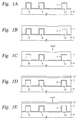
- Fig.1A-1E illustrates a three-layer deposition PECVD process for depositing a PECVD lining layer 2 of the oxidized organosilane or organosiloxane polymer as described in International Publication Number WO 99/41423.
- the lining layer 2 acts as an isolation layer between a subsequent layer 7 and the underlying substrate surface 6 and metal lines 8, 9, 10 formed on the substrate surface.
- the layer 7 is capped by a PECVD capping layer 12 of the oxidized organosilane or organosiloxane polymer.
- the PECVD process deposits a multi-component dielectric layer, wherein an carbon containing silicon dioxide (SiO 2 ) is first deposited on the patterned metal layer having metal lines 8, 9, 10 formed on substrate 6.
- the PECVD lining layer 2 is deposited by the plasma enhanced reaction of an organosilane or organosiloxane compound such as methylsilane, CH 3 SiH 3 , and an oxidizing gas such as N 2 O in the presence of an inert gas, such as argon, at a temperature of approximately -20°C to 40°C.
- an inert gas such as argon
- the oxidized organosilane or organosiloxane layer is then cured.
- the deposited PECVD lining layer 2 (at about 2000 ⁇ per minute) has improved barrier characteristics for the subsequent deposition of the layer 7 shown in Fig. 1B.
- the lining layer obtained from methylsilane has sufficient C-H bonds to be hydrophobic, and is an excellent moisture barrier.
- a low K dielectric layer 7 is then deposited on the liner layer 2 by the reaction of a silane compound and hydrogen peroxide (H 2 O 2 ) at a temperature below 200°C at a pressure of about 0.2 to about 5 Torr during deposition of the layer 7.
- the layer 7 may be partially cured as shown in Fig. 1C to remove solvents such as water prior to deposition of a cap layer 12 as shown in Fig. 1D. Curing is performed by pumping down a reaction under an inert gas atmosphere under 10 Torr.
- an optional capping layer 12 may be deposited on the low k dielectric layer 7 by the plasma enhanced reaction of an organosilane or organosiloxane compound and an oxidizing gas such as N 2 O.
- an oxidizing gas such as N 2 O.
- the capping layer 12 is also an oxidized organosilane or organosiloxane film that has good barrier properties and has a dielectric property of about 3.0. Both the liner layer 2 and the cap layer 12 have a dielectric constant greater than 3.0 and the high dielectric constant layers substantially detract from the benefit of the low k dielectric layer 7.
- Lowering the parasitic capacitance between metal interconnects separated by dielectric material can be accomplished by either increasing the thickness of the dielectric material or by lowering the dielectric constant of the dielectric material. Increasing the thickness of the dielectric materials, however, does not address parasitic capacitance within the same metallized layer or plane. As a result, to reduce the parasitic capacitance between metal interconnects on the same or adjacent layers, one must change the material used between the metal lines or interconnects to a material having a lower dielectric constant than that of the materials currently used, i . e ., k ⁇ 3.0.
- the present invention provides a method for depositing a nano-porous silicon oxide layer having a low dielectric constant.
- the nano-porous silicon oxide layer is produced by depositing a silicon/oxygen containing material that further contains thermally labile organic groups, and by controlled annealing of the deposited silicon/oxygen containing material to form microscopic gas pockets, or voids, that are uniformly dispersed in a silicon oxide layer.
- the relative volume of the microscopic gas pockets to the silicon oxide layer is controlled to preferably maintain a closed cell foam structure that provides low dielectric constants.
- the silicon/oxygen material is deposited by plasma enhanced chemical vapor deposition of one or more compounds comprising at least one oxidizable silicon containing component and at least one non-silicon containing component having thermally labile groups.
- the labile groups in the reactive compound or mixture contain sufficient oxygen to convert to gaseous products to evolve from the film and leave voids when the deposited silicon oxide layer is annealed.
- the oxidizable silicon containing component can be separated from non-silicon components having thermally labile groups in the same molecule.
- Preferred silicon-oxygen ligands of components that form nano-porous silicon oxide-based layers under controlled annealing comprise methylsiloxy (CH 3 -SiH 2 -O-) or dimethylsiloxy ((CH 3 ) 2 -SiH-O-) groups.
- Preferred compounds formed from these components include methylsilyl-1,4-dioxinyl ether or methylsiloxanyl furan. Formation of voids using 2,4,6-trisilaoxane and cyclo-1,3,5,7-tetrasilano-2,6-dioxy-4,8-dimethylene is enhanced by virtue of their non-planar ring structure.
- Such compounds react with an oxidizing gas to form a silicon/oxygen containing material that retains many of the labile organic groups at temperatures below about 50°C.
- the amount of labile groups can be increased by mixing the reactive compounds with non-silicon containing components that comprise one or more labile groups, such as vinyl-1,4-dioxinyl ether, vinyl furyl ether, vinyl-1,4-dioxin, vinyl furan, methyl furoate, furyl formate, furyl acetate, furaldehyde, difuryl ketone, difuryl ether, difurfuryl ether, furan, 1,4- dioxin, fluorinated derivatives thereof, and combinations thereof.
- labile groups such as vinyl-1,4-dioxinyl ether, vinyl furyl ether, vinyl-1,4-dioxin, vinyl furan, methyl furoate, furyl formate, furyl acetate, furaldehyde, difuryl ket
- the non-silicon containing components can alternatively be mixed with the reactive silicon containing materials that do not contain thermally labile organic groups, such as methylsilane, dimethylsilane, 1,1,3,3-tetramethyldisiloxane, 1,1,5,5-tetramethyltrisiloxane, disilanomethane, and fluorinated carbon derivatives thereof.
- thermally labile organic groups such as methylsilane, dimethylsilane, 1,1,3,3-tetramethyldisiloxane, 1,1,5,5-tetramethyltrisiloxane, disilanomethane, and fluorinated carbon derivatives thereof.
- the silicon/oxygen containing material is preferably deposited by striking a plasma at an RF power level from 10-250 W in an oxidizing gas selected from the group consisting of N 2 O, O 2 , O 3 , CO 2 , and combinations thereof.
- the deposited silicon/oxygen containing material is then annealed at a gradually increasing temperature profile to convert the labile organic groups to dispersed gas pockets in a nano-porous silicon oxide layer having a low dielectric constant attributed to a preferably closed cell foam structure. Annealing preferably increases the temperature of the deposited material to about 350°C to about 400°C.
- the nano-porous silicon oxide layer of the present invention is deposited on a PECVD silicon oxide, silicon nitride, silicon oxynitride, or hydrogenated silicon carbide barrier layer that was deposited on a patterned metal layer by plasma assisted reaction of one or more reactive silicon containing compounds.
- the nano-porous silicon oxide layer is then deposited in the same chamber or in an adjacent cluster tool processing chamber. After annealing as described above, the nano-porous silicon oxide layer is capped in the same chamber or in an adjacent cluster tool processing chamber with PECVD silicon oxide, silicon nitride, silicon oxynitride, or hydrogenated silicon carbide.
- the liner and cap layers serve as barriers which protect the nano-porous silicon oxide layer.
- the present invention provides a method for depositing a nano-porous silicon oxide layer having a low dielectric constant.
- the nano-porous silicon oxide layer is produced by plasma enhanced (PECVD) or microwave enhanced chemical vapor deposition of a silicon/oxygen containing material that optionally contains thermally labile organic groups, and by controlled annealing of the deposited silicon/oxygen containing material to form microscopic gas pockets that are uniformly dispersed in a silicon oxide layer.
- the relative volume of the microscopic gas pockets to the silicon oxide layer is controlled to preferably maintain a closed cell foam structure that provides low dielectric constants after annealing.
- the nano-porous silicon oxide layers will have dielectric constants less than about 2.5, preferably less than about 2.0.
- the silicon/oxygen material is chemical vapor deposited by reacting an oxidizable silicon containing compound or mixture comprising an oxidizable silicon component and an unsaturated non-silicon bearing component having thermally labile groups with an oxidizing gas.
- the oxidizing gases are oxygen (O 2 ) or oxygen containing compounds such as nitrous oxide (N 2 O), ozone (O 3 ), and carbon dioxide (CO 2 ), preferably N 2 O or O 2 .
- Oxygen and oxygen containing compounds are preferably dissociated to increase reactivity when necessary to achieve a desired carbon content in the deposited film.
- RF power can be coupled to the deposition chamber to increase dissociation of the oxidizing compounds.
- the oxidizing compounds may also be dissociated in a microwave chamber prior to entering the deposition chamber to reduce excessive dissociation of the silicon containing compounds.
- Deposition of the silicon oxide layer can be continuous or discontinuous. Although deposition preferably occurs in a single deposition chamber, the layer can be deposited sequentially in two or more deposition chambers.
- RF power can be cycled or pulsed to reduce heating of the substrate and promote greater porosity in the deposited film.
- the oxidizable silicon component of the oxidizable silicon containing compound or mixture comprises organosilane or organosiloxane compounds which generally include the structure: wherein each Si is bonded to at least one hydrogen atom and may be bonded to one or two carbon atoms, and C is included in an organo group, preferably alkyl or alkenyl groups such as-CH 3 , -CH 2 -CH 3 , -CH 2 -, or -CH 2 -CH 2 -, or fluorinated carbon derivatives thereof.
- an organosilane or organosiloxane compound includes two or more Si atoms
- each Si is separated from another Si by -O-, -C-, or -C-C-, wherein each bridging C is included in an organo group, preferably alkyl or alkenyl groups such as -CH 2 -, -CH 2 -CH 2 -, -CH(CH 3 )-, -C(CH 3 ) 2 -, or fluorinated carbon derivatives thereof.
- the preferred organosilane and organosiloxane compounds are gases or liquids near room temperature and can be volatilized above about 10 Torr.
- Suitable silicon containing compounds include: methylsilane, CH 3 -SiH 3 dimethylsilane, (CH 3 ) 2 -SiH 2 disilanomethane, SiH 3 -CH 2 -SiH 3 bis(methylsilano)methane, CH 3 -SiH 2 -CH 2 -SiH 2 -CH 3 2,4,6-trisilaoxane -(-SiH2-CH 2 -SiH 2 -CH 2 -SiH 2 -O-)- (cyclic) cyclo-1,3,5,7-tetrasilano-2,6-dioxy-4,8-dimethylene -(-SiH 2 -CH 2 -SiH 2 -O-)2- (cyclic) 1,3,5-trisilacyclohexane, -(-SiH 2 -CH 2 -) 3 - (cyclic) 1,3-dimethyldisiloxane, CH 3 -S
- the hydrocarbon groups in the organosilanes and organosiloxane may be partially or fully fluorinated to convert C-H bonds to C-F bonds.
- Many of the preferred organosilane and organosiloxane compounds are commercially available.
- a combination of two or more of the organosilanes or organosiloxanes can be employed to provide a blend of desired properties such as dielectric constant, oxide content, hydrophobicity, film stress, and plasma etching characteristics.
- the organosilane or organosiloxane compound are functional groups possessing both a silicon oxygen bond and a silicon-hydrogen bond.
- Preferred functional groups having the bonding requirements include: methylsiloxy, and (CH 3 -SiH 2 -O-) dimethylsiloxy ((CH 3 ) 2 -SiH-O-)
- the unsaturated non-silicon bearing component having thermally labile groups has the property of reacting with an plasma-sustained oxidizing environment to form thermally labile molecules that deposit, and which, when subsequently exposed to elevated temperatures, thermally decompose to form volatile species with low boiling points. Decomposition and evolution of the thermally labile group's volatile species from the deposited film will leave voids in the structure, reducing the structure's density. Selectively removing embedded chemically reacted solid material within the deposited film by a thermal process results in low density films which have low dielectric constants.
- Formation of voids using some compounds such as 2,4,6-trisilaoxane (2,4,6-trisilatetrahydropyran) and cyclo-1,3,5,7-tetrasilano-2,6-dioxy-4,8-dimethylene is achieved during annealing without addition of labile groups by virtue of a non-planar ring structure: 1,3,5,7-tetrasilano-2,6-dioxy-4,8-dimethylene, and -(-SiH 2 -CH 2 -SiH 2 -O-) 2 - (cyclic) 2,4,6-trisilatetrahydropyran, -SiH 2 -CH 2 -SiH 2 -CH 2 -SiH 2 -O-(cyclic)
- the thermally labile organic groups contain sufficient oxygen to form gaseous products when the silicon oxide layer is annealed.
- thermally labile groups are non-silicon containing multiply unsaturated cycloalkanes (having two or more carbon-carbon double bonds), including heterocyclodialkenes, with oxygen or nitrogen incorporated within the molecular structure, and which generally tend to perform favorably in plasma environments.
- the compounds are liquid at room temperature and can be volatilized near a pressure of 10 Torr or above.
- Such compounds react with an oxidizing gas to form a gel-like silicon/oxygen containing material that retains many of the labile organic groups at temperatures below about 50°C.
- the amount of labile organic groups retained in the deposited silicon/oxygen containing material can be increased by mixing the reactive compounds with non-silicon containing components that comprise one or more labile organic groups.
- the labile organic groups include the dioxan, furan, and fulvene derivative chemicals described for the silicon containing reactive compounds and other oxygen containing organic groups.
- the labile organic groups are preferably the silicon containing and non-silicon containing components incorporated in the same molecule, but with the methylsilyl or methylsiloxanyl groups replaced with vinyl groups, or with the methylsiloxanyl groups replaced with ester groups, or with the methylsiloxanyl groups replaced with other non-silicon containing organic groups, in addition to those chemicals without the methylsiloxanyl groups, such as 1,4-dioxin and furan.
- the non-silicon containing components can alternatively be mixed with the reactive silicon containing materials that do not contain labile organic groups, such as: methylsilane, CH 3 -SiH 3 dimethylsilane, (CH 3 ) 2 -SiH 2 disilanomethane, SiH 3 -CH 2 -SiH 3 bis(methylsilano)methane, CH 3 -SiH 2 -CH 2 -SiH 2 -CH 3 2,4,6-trisilaoxane -(-SiH 2 -CH 2 -SiH 2 -CH 2 -SiH 2 -O-)- (cyclic) 1,3,5-trisilacyclohexane, -(-SiH 2 CH 2 -) 3 - (cyclic) cyclo-1,3,5,7-tetrasilano-2,6-dioxy-4,8-dimethylene -(-SiH 2 -CH 2 -SiH 2 -O
- thermally-labile-imparting and non-thermally-labile-imparting compounds can be co-deposited to tailor film properties.
- a preferred embodiment of the codeposition compounds include a thermally-labile-imparting compound selected from either methylsilyl-1,4-dioxinyl ether or 2-methylsiloxanyl furan and a non-thermally-labile-imparting compound selected from either 2,4,6-trisilaoxane (2,4,6-trisilatetrahydropyran) or cyclo-1,3,5,7-tetrasilano-2,6-dioxy-4,8-dimethylene.
- the co-deposited heteroalicyclic non-thermally-labile imparting molecules which can be used advantageously are non-planar cyclic molecules with insignificant ring strain and which deposit in random orientations.
- the dual bonding of the silyl functional groups to the methylene groups can provide improved thermal stability and better mechanical properties of the resultant film.
- the non-planar molecule can provide a relatively reduced stack density within the deposited film, thereby producing low dielectric films.
- the film is preferably annealed at a gradually increasing temperature to convert the labile organic groups to dispersed gas pockets in a nano-porous silicon oxide layer having a low dielectric constant attributed to a preferably closed cell foam structure.
- the nano-porous silicon oxide layer of the present invention is deposited on a PECVD silicon oxide, silicon nitride, silicon oxynitride, or hydrogenated silicon carbide (e.g., BLOkTM layer material available from Applied Materials Inc., of Santa Clara, California.) barrier layer that was deposited on a patterned metal layer by plasma assisted reaction of one or more reactive silicon containing compounds.
- the nano-porous silicon oxide layer is then deposited in the same multichamber clustered CVD system while applying RF power or remote microwave power, and is subsequently heated using an increasing temperature profile, optionally to between about 350°C to about 400°C.
- the nano-porous silicon oxide layer is optionally capped in the same chamber or in an adjacent cluster tool processing chamber used to deposit the barrier layer, for example with a hydrogenated silicon carbide (BLOkTM).
- BLOkTM hydrogenated silicon carbide
- the liner and cap layers serve as barriers which protect the nano-porous silicon oxide layer.
- the chemical used is preferably selected from a group consisting of hexamethyldisilazane, trimethylsilyldiethylamine, phenyldimethylsilyldimethylamine, trimethoxysilyldi-methylamine, tris(trifluoromethyl)silyldimethylamine, bis(trimethyl-silyl)hydrazine, 1-phenyldimethylsilyl-2-methyl-hydrazine, 1-trimethoxysilyl-2-methyl-hydrazine, 1-tris(trifluoromethylsilyl)-2-methyl-hydrazine, trimethylchlorosilane, trimethylbromosilane, trimethylsilane, or combinations thereof.
- the liner and cap layers can be deposited by plasma assisted chemical vapor deposition (CVD) of silicon oxide, silicon nitride, silicon oxynitride, or hydrogenated silicon carbide (BLOkTM).
- CVD plasma assisted chemical vapor deposition
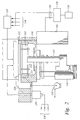
- a suitable CVD plasma reactor in which a method of the present invention can be carried out is the "DLK" chamber available from Applied Materials of Santa Clara, California, and is shown in Fig. 2, which is a vertical, cross-section view of a parallel plate chemical vapor deposition reactor 110 having a high vacuum region 115.
- Reactor 110 contains a gas distribution manifold 111 for dispersing process gases through perforated holes in the manifold to a substrate or substrate (not shown) that rests on a substrate support plate or susceptor 112 which is raised or lowered by a lift motor 114.
- a liquid injection system (not shown), such as typically used for liquid injection of TEOS, may also be provided for injecting a liquid reactant.
- Preferred liquid injection systems include the AMAT Gas Precision Liquid Injection System (GPLIS) and the AMAT Extended Precision Liquid Injection System (EPLIS), both available from Applied Materials, Inc.
- GPLIS AMAT Gas Precision Liquid Injection System
- EPLIS AMAT Extended
- the reactor 110 includes heating of the process gases and substrate, such as by resistive heating coils (not shown) or external lamps (not shown).
- susceptor 112 is mounted on a support stem 113 so that susceptor 112 (and the substrate supported on the upper surface of susceptor 112) can be controllably moved between a lower loading/off-loading position and an upper processing position which is closely adjacent to manifold 111.
- susceptor 112 and the substrate When susceptor 112 and the substrate are in processing position 114, they are surrounded by a an insulator 117 and process gases exhaust into a manifold 124. During processing, gases inlet to manifold 111 are uniformly distributed radially across the surface of the substrate.
- a vacuum pump 132 having a throttle valve controls the exhaust rate of gases from the chamber.
- deposition and carrier gases are input through gas lines 118 into a mixing system 119 where they are combined and then sent to manifold 111.
- An optional microwave system 150 (shown in Fig. 3) having a applicator tube 120 may be located on the input gas line for the oxidizing gas to provide additional energy that dissociates only the oxidizing gas prior to entry to the reactor 110.
- the microwave applicator provides a power from between about 0 and about 6000 W.
- the process gases supply lines 18 for each of the process gases include (i) safety shut-off valves (not shown) that can be used to automatically or manually shut off the flow of process gas into the chamber, and (ii) mass flow controllers (also not shown) that measure the flow of gas through the gas supply lines.
- safety shut-off valves not shown
- mass flow controllers also not shown
- the deposition process performed in reactor 110 can be either a non-plasma process on a cooled substrate pedestal or a plasma enhanced process.
- a controlled plasma is typically formed adjacent to the substrate by RF energy applied to distribution manifold 111 from RF power supply 125 (with susceptor 112 grounded).
- RF power can be provided to the susceptor 112 or RF power can be provided to different components at different frequencies.
- RF power supply 125 can supply either single or mixed frequency RF power to enhance the decomposition of reactive species introduced into the high vacuum region 115.
- a mixed frequency RF power supply typically supplies power at a high RF frequency (RF1) of about 13.56 MHz to the distribution manifold 111 and at a low RF frequency (RF2) of about 360 KHz to the susceptor 112.
- RF1 high RF frequency
- RF2 low RF frequency
- the silicon oxide layers of the present invention are most preferably produced using low levels or pulsed levels of high frequency RF power.
- Pulsed RF power preferably provides 13.56 MHz RF power at about 20 to about 200 W during about 10% to about 30% of the duty cycle.
- Non-pulsed RF power preferably provides 13.56 MHz RF power at about 10 to about 150 W as described in more detail below.
- Low power deposition preferably occurs at a temperature range from about -20 to about 40°C. At the preferred temperature range, the deposited film is partially polymerized during deposition and polymerization is completed during subsequent curing of the film.
- an optional microwave chamber can be used to input from about 0 to about 3000W of microwave power to the oxidizing gas prior to entering the deposition chamber. Separate addition of microwave power would avoid excessive dissociation of the silicon compounds prior to reaction with the oxidizing gas.
- a gas distribution plate having separate passages for the silicon compound and the oxidizing gas is preferred when microwave power is added to the oxidizing gas.
- any or all of the chamber lining, gas inlet manifold faceplate, support stem 113, and various other reactor hardware is made out of material such as aluminum or anodized aluminum.
- An example of such a CVD reactor is described in U.S. Patent 5,000,113, entitled “Thermal CVD/PECVD Reactor and Use for Thermal Chemical Vapor Deposition of Silicon Dioxide and In-situ Multi-step Planarized Process,” issued to Wang et al . and assigned to Applied Materials. Inc., the assignee of the present invention.
- the lift motor 114 raises and lowers susceptor 112 between a processing position and a lower, substrate-loading position.
- the motor, the gas mixing system 119, and the RF power supply 125 are controlled by a system controller 134 over control lines 136.
- the reactor includes analog assemblies, such as mass flow controllers (MFCs) and standard or pulsed RF generators, that are controlled by the system controller 134 which executes system control software stored in a memory 210, which in the preferred embodiment is a hard disk drive.
- MFCs mass flow controllers
- RF generators standard or pulsed RF generators
- the system controller 134 controls all of the activities of the CVD reactor and a preferred embodiment of the controller 134 includes a hard disk drive, a floppy disk drive, and a card rack.
- the card rack contains a single board computer (SBC), analog and digital input/output boards, interface boards and stepper motor controller boards.
- SBC single board computer
- the system controller conforms to the Versa Modular Europeans (VME) standard which defines board, card cage, and connector dimensions and types.
- VME Versa Modular Europeans
- the VME standard also defines the bus structure having a 16-bit data bus and 24-bit address bus.
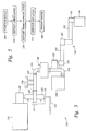
- Fig. 3 is a simplified diagram of a remote microwave system 150 for dissociating process gases such as water prior to entering the DLK reactor 110, in accordance with an embodiment of the present invention.
- Remote microwave system 150 includes an applicator tube 120, a plasma ignition system including an ultraviolet (UV) lamp 154 and a UV power supply 155, a microwave waveguide system that includes various lengths of straight and curved waveguide sections 156, waveguide coupling 158, which may be connected together at joints 157, an output waveguide section 160, and a magnetron 168.
- the waveguide section 156 may further have an arm support 162 formed therein for attachment to an pivoting arm 164 mounted on a arm base 166.
- the pivoting arm comprises arm pieces 165 coupled to arm joints 163 that provide vertical separation of the arm pieces and allow rotational movement of the arm 164 around the arm joints 163.
- the arm joints 163, are vertically disposed cylinders coupled to one arm piece 165 at the bottom of the arm joint 163 and coupled to a second arm piece 165 at the top of the arm joint 165.
- the attachment of the arm pieces 165 at the ends of the arm joint 163 allow for vertical separation of the arm pieces and flexibility of position the arm 164, and thus the microwave system 150, during operation and maintenance of the processing reactor 110.
- Magnetron 168 is a typical magnetron source capable of operating between about 0-3000 Watts for continuous wave (CW) or pulsed output of microwaves of about 2.45 Gigahertz (GHz) frequency. Of course, other magnetrons may be utilized as well. Circulator (not shown) allows only forward microwave transmission from magnetron 168 toward applicator tube 120.
- Tuning system 170 which may use stub tuners or other tuning elements, provides the microwave system 150 with the ability to match the load at waveguide section 160 to the characteristic impedance of the waveguides. Tuning system 170 may provide fixed tuning, manual tuning, or automated tuning, according to specific embodiments. In the specific embodiment, the waveguide sections have rectangular cross-sections, but other types of waveguide also may be used.
- Applicator tube 120 is a circular (or other cross-section) tube made of a composite or ceramic material, preferably alumina, or other material resistant to etching by radicals.
- applicator tube 120 has a length of about 18-24 inches and a cross-sectional diameter of about 3-4 inches.
- Applicator tube 120 is disposed through a waveguide section 160, which is open at one end for transmitting microwaves and is terminated at the other end with a metal wall. Microwaves are transmitted through the open end of waveguide section 160 to gases inside applicator tube 120, which is transparent to microwaves.
- other materials such as sapphire also may be used for the interior of applicator tube 120.
- applicator tube 120 may have a metal exterior and an interior made of a composite or ceramic material wherein microwaves in waveguide section 160 enter a window through the exterior of applicator tube 120 to the exposed interior of tube 120 to energize the gases.
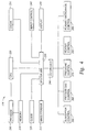
- Fig. 4 shows a block diagram of a processing system, or reactor 110, such as that depicted in Fig. 2, having such a system controller 134 that can be employed in such a capacity.
- the system controller 134 includes a programmable central processing unit (CPU) 220 that is operable with a memory 210, a mass storage device 215, an input control unit 245, and a display unit 255.
- CPU central processing unit
- the system controller further includes well-known support circuits 214 such as power supplies, clocks 225, cache 235, input/output (I/O) circuits 240 and the like, coupled to the various components of the DLK process reactor 110 to facilitate control of the deposition process.
- the controller 134 also includes hardware for monitoring substrate processing through sensors (not shown) in the chamber 110. Such sensors measure system parameters such as substrate temperature, chamber atmosphere pressure and the like. All of the above elements are coupled to a control system bus 230.
- the CPU 220 may be one of any form of general purpose computer processor that can be used in an industrial setting for controlling various chambers and subprocessors.
- the memory 210 is coupled to the CPU 220, and is accessible to the system bus 230.
- the memory 210, or computer-readable medium 215, may be one or more of readily available memory such as random access memory (RAM), read only memory (ROM), floppy disk drive, hard disk, or any other form of digital storage, local or remote.
- the support circuits 214 are coupled to the CPU 220 for supporting the processor in a conventional manner.
- the deposition process is generally stored in the memory 210, typically as a software routine.
- the software routine may also be stored and/or executed by a second CPU (not shown) that is remotely located from the hardware being controlled by the CPU 220.
- the memory 210 contains instructions that the CPU 220 executes to facilitate the performance of the processing system 10.
- the instructions in the memory 210 are in the form of program code such as a program 200 that implements the method of the present invention.
- the program code may conform to any one of a number of different programming languages. For example, the program code can be written in C, C++, BASIC, Pascal, or a number of other languages.
- the mass storage device 215 stores data and instructions are retrieves data and program code instructions from a processor readable storage medium, such as a magnetic disk or magnetic tape.
- a processor readable storage medium such as a magnetic disk or magnetic tape.
- the mass storage device 215 can be a hard disk drive, floppy disk drive, tape drive, or optical disk drive.
- the mass storage device 215 stores and retrieves the instructions in response to directions that it receives from the CPU 220.
- Data and program code instructions that are stored and retrieved by the mass storage device 215 are employed by the processor unit 220 for operating the processing system.
- the data and program code instructions are first retrieved by the mass storage device 215 from a medium and then transferred to the memory 210 for use by the CPU 220.
- the input control unit 245 couples a data input device, such as a keyboard, mouse, or light pen, to the processor unit 220 via the system bus 230 to provide for the receipt of a chamber operator's inputs.
- the display unit 255 provides information to a chamber operator in the form of graphical displays and alphanumeric characters under control of the CPU 220.
- the control system bus 230 provides for the transfer of data and control signals between all of the devices that are coupled to the control system bus 230.
- the control system bus is displayed as a single bus that directly connects the devices in the CPU 220, the control system bus 230 can also be a collection of busses.
- the display unit 255, input control unit 245 (with input device), and mass storage device 215 can be coupled to an input-output peripheral bus, while the CPU 220 and memory 210 are coupled to a local processor bus.
- the local processor bus and input-output peripheral bus are coupled together to form the control system bus 230.
- the system controller 134 is coupled to the elements of the processing system 10, employed in dielectric deposition processes in accordance with the present invention via the system bus 230 and the I/O circuits 240.
- the I/O circuits 240 receive instructions from the program 200 stored in memory 210 via the CPU 220 and system bus 230.
- the program 200 provides program subroutines that enable the I/O circuits 240 to provide for substrate positioning control 250, process gas control 260, pressure control 270, heater control 280, and plasma/microwave control 290, of the reactor 110.
- the CPU 220 forms a general purpose computer that becomes a specific purpose computer when executing programs such as the program 200 of the embodiment of the method of the present invention depicted in the flow diagram of Fig. 4.
- programs such as the program 200 of the embodiment of the method of the present invention depicted in the flow diagram of Fig. 4.
- ASIC application specific integrated circuit
- CVD system description is mainly for illustrative purposes, and other plasma CVD equipment such as electrode cyclotron resonance (ECR) plasma CVD devices, induction-coupled RF high density plasma CVD devices, or the like may be employed. Additionally, variations of the above described system such as variations in susceptor design, heater design, location of RF power connections and others are possible. For example, the substrate could be supported and heated by a resistively heated susceptor.
- ECR electrode cyclotron resonance
- the pretreatment and method for forming a pretreated layer of the present invention is not limited to any specific apparatus or to any specific plasma excitation method.
- the nano-porous silicon oxide layer of the present invention can be deposited in a three-layer process as shown in Fig. 5 using the PECVD or microwave chamber of Fig. 2.
- a substrate is positioned 300 in the reactor 110 and a barrier layer is deposited 305 by a PECVD process from a plasma comprising a reactive silicon containing compound.
- the deposition step 305 can include a capacitively coupled plasma or both an inductively and a capacitively coupled plasma in the process chamber 15 according to methods known in the art.
- An inert gas such as helium is commonly used in the PECVD deposition to assist in plasma generation.
- a nano-porous layer of the present invention is then deposited 310 on the liner layer by depositing a silicon/oxygen containing material that further contains labile organic groups, and by controlled annealing of the deposited silicon/oxygen containing material to form microscopic gas pockets that are uniformly dispersed in the layer.
- a cap layer is then deposited 315 on the layer, preferably using a similar process as employed for depositing the lining layer.
- the substrate is then removed 320 from the reactor 110.
- the three-layer process provides a PECVD lining layer 400.
- the lining layer 400 acts as an isolation layer between the subsequent nano-porous layer 402 and the underlying substrate surface 404 and metal lines 406, 408, 410 formed on the substrate surface.
- the nano-porous layer 402 is capped by a PECVD capping layer 412 of the silicon containing compound. This process is implemented and controlled using a computer program stored in the memory 220 of a computer controller 134 for a CVD reactor 110.
- the PECVD lining layer 400 is deposited in the reactor 110 by introducing a reactive silicon containing compound and an oxidizing gas.
- the process gases react in a plasma enhanced environment to form a conformal silicon oxide layer 400 on the substrate surface 404 and metal lines 406, 408, 410.
- the nano-porous layer 402 is deposited from a processing gas consisting of silicon and labile containing compounds and an oxidizing gas.
- the process gas flows range from about 20 to about 1000 sccm for the silicon and labile containing compounds, and about 5 to about 4000 sccm of the oxidizing gas.
- the preferred gas flows range from about 50 to about 500 sccm for the silicon and labile containing compounds and a flow rate of about 5 to about 2000 sccm of the oxidizing gas. These flow rates are given for a chamber having a volume of approximately 5.5 to 6.5 liters.
- reactor 110 is maintained at a pressure of about 0.2 to about 5 Torr during deposition of the nano-porous layer 402.
- the nano-porous layer 402 is cured as shown in Fig. 6C to remove volatile constituents prior to deposition of a cap layer 412 as shown in Fig. 6D. Curing can be performed in the reactor 110 under an inert gas atmosphere while heating the substrate to progressively higher temperatures.
- the nano-porous layer 402 is preferably annealed at a gradually increasing temperature to retain gaseous products as dispersed microscopic bubbles, and/or to convert the optional labile organic groups to dispersed microscopic gas bubbles that are retained in the cured silicon oxide film as voids in a preferably closed cell structure.
- a preferred anneal process comprises a heating time period of about 5 minutes, including gradually raising the temperature by about 50°C/min. to a final temperature of between about 350°C to about 400°C.
- Dispersion of the gas bubbles can be controlled by varying the temperature/time profile and by controlling the concentration of labile organic groups in the deposited film.
- the reactor 110 deposits a capping layer 412, preferably of the same material and by the same methods as used for the deposition of the PECVD liner layer 400.
- a capping layer 412 preferably of the same material and by the same methods as used for the deposition of the PECVD liner layer 400.
- the deposited layers are further annealed in a furnace or another chamber at a temperature from about 200°C to about 450°C to drive off remaining volatile products such as water.
- processing conditions will vary according to the desired characteristics of the deposited films.
- FIG. 7 A preferred dual damascene structure 500 fabricated in accordance with the invention is shown in Fig. 7, and the method of making the structure is sequentially depicted schematically in Figs.8A-8H, which are cross sectional views of a substrate having the steps of the invention formed thereon.
- a dual damascene structure 500 which includes a nano-porous intermetal dielectric layer 510 is shown in Fig 7.
- the intermetal dielectric layers 510 and 514 deposited according to the invention have extremely low dielectric constants of less than 3, and are often referred to as extreme low k, or ELk, dielectric layers.
- a first dielectric layer 510, preferably consisting of the nano-porous silicon oxide layer of the present invention is deposited on a substrate 502.
- the substrate comprising patterned conducting lines 506 formed in a contact level substrate material 504, with a first (or substrate) etch stop 508 of silicon oxide, silicon nitride, silicon oxynitride, or amorphous hydrogenated silicon carbide (BLOkTM), preferably silicon nitride, deposited thereon.
- BLOkTM amorphous hydrogenated silicon carbide
- a silicon oxide, silicon nitride, silicon oxynitride, or hydrogenated silicon carbide (BLOkTM) second etch stop 512 is deposited on the first dielectric layer 510.
- a second dielectric layer 514 preferably consisting of the nano-porous silicon oxide layer of the present invention is deposited on the second etch stop 512, with a third etch stop 516 deposited on the second dielectric layer 514.
- the deposited layers are etched to form a via 520, which is subsequently filled with a conducting metal 524, preferably copper, over a barrier layer 522 conformally deposited within the via 520.
- the structure is then planarized and a capping layer 518 comprising silicon nitride, silicon oxide, silicon oxynitride, or hydrogenated silicon carbide, preferably comprising silicon nitride, is deposited thereon.
- the capping layer 518 also serves as the substrate etch stop and corresponds to the first etch stop 508 for subsequent dual damascene multilevel interconnects.
- a first (or substrate) etch stop 508 of silicon oxide, silicon nitride, silicon oxynitride, or amorphous hydrogenated silicon carbide, preferably silicon nitride is deposited to a thickness of about 1000 ⁇ on the substrate 502.
- the substrate 502 comprises patterned conducting interconnects or lines 506 formed in a contact level substrate material 504.
- a first nano-porous dielectric layer 510 is deposited according to the invention on the first etch stop 508.
- the first dielectric layer 510 has a thickness of about 5,000 ⁇ to about 10,000 ⁇ , depending on the size of the structure to be fabricated, but has a preferable thickness of about 5,000 ⁇ .
- the first dielectric layer 510 and is then annealed at a temperature of about 350°C to about 400°C to remove volatile contaminants from the layer 510.
- a second etch stop 512 such as silicon oxynitride, is deposited on the dielectric layer 510 to a thickness of about 500 ⁇ .
- a second nano-porous dielectric layer 514 is then deposited a thickness of about 5,000 ⁇ to about 10,000 ⁇ , preferably about 5,000 ⁇ , according to the invention on the first etch stop 508, and is then annealed at a temperature of about 350°C to about 400°C.
- An anti-reflective coating (ARC) 519 and a trench photomask comprising a photoresist layer 521 are then respectfully deposited over the silicon oxide layer 517.
- the photoresist layer 521 is then patterned by conventional photolithography means known in the art.
- the silicon oxide layer 517 is then etched by conventional means known in the art, preferably by an etch process using fluorocarbon chemistry, to expose the third etch 516 as shown in Fig. 8B.
- the initial etch of the silicon oxide layer 517 establishes the opening width, or trench width, of the dual damascene structure 500.
- the opening width formed in the silicon oxide layer 517 defines the horizontal interconnect of the dual damascene structure 500 formed above the second etch stop 514.
- the remaining photoresist 521 is then ashed, or dry removed, for preparation of the via etch.
- a second anti-reflective coating 519 and a photoresist layer 521 are then respectfully deposited over the thin silicon oxide layer 517, and then patterned by photolithography to expose the third etch layer 516 by the via width as shown in Fig. 8C.
- the third etch stop 516 and second dielectric layer 514 are trenched etched to expose the second etch stop 512.
- the via 520 is then formed by via etching the second dielectric layer 514 to the second etch stop 512 using anisotropic etching techniques to define the metallization structure ( i . e ., the interconnect and contact/via) at the width established by the silicon oxide layer 517; and etching the first dielectric layer 510 to the first etch stop 508 at the via width established during the etching of the third etch stop 516, second dielectric layer 514, and the second etch stop 512 as shown in Fig. 8E.
- Fig. 8F shows the etching of the first etch stop 508 protecting the substrate 502, exposing the underlying patterned metal lines 506 in the contact level substrate material 504.
- the patterned metal lines 506 preferably comprise a conducting metal such as copper.
- the dual damascene structure 500 is then precleaned by conventional means known in the art prior to subsequent layer deposition.
- the metallization structure is then formed with a conductive material such as aluminum, copper, tungsten or combinations thereof.
- a conductive material such as aluminum, copper, tungsten or combinations thereof.
- the trend is to use copper to form the smaller features due to the low resistivity of copper (1.7 mW-cm compared to 3.1 mW-cm for aluminum).
- a suitable barrier layer 522 such as tantalum nitride is first deposited conformally in the metallization pattern 520 to prevent copper migration into the surrounding silicon and/or dielectric material.
- a layer of copper 524 is deposited using either chemical vapor deposition, physical vapor deposition, electroplating, preferably by electroplating, to form the conductive structure.
- the surface is planarized using chemical mechanical polishing and capped with a capping layer 518, preferably comprising silicon nitride and having a thickness of about 1000 ⁇ , as shown in Fig. 8H.
- a capping layer 518 preferably comprising silicon nitride and having a thickness of about 1000 ⁇ , as shown in Fig. 8H.
- the metal Prior to planarizing the surface, the metal may be annealed in a hydrogen atmosphere to recrystallize the copper fill and to remove voids that may have formed in the structure 500.
- a copper seed layer may be deposited prior to the copper layer 524 when the copper layer 524 is deposited by an electroplating process.
- the dual damascene formation process may then be repeated to deposit further interconnection levels, of which modern microprocessor integrated circuits have 5 or 6 interconnection levels.
- the following examples demonstrate deposition of a nano-porous silicon oxide based film having dispersed microscopic gas voids. This example is undertaken using a chemical vapor deposition chamber, and in particular, a CENTURA "DLK" system fabricated and sold by Applied Materials, Inc., Santa Clara, California.
- a nano-porous silicon oxide based film is deposited at a chamber pressure of 1.0 Torr and temperature of 30°C from reactive gases which are vaporized and flown into the reactor as follows: methylsilyl-2-furyl ether, at 150 sccm nitrous oxide (N 2 O), at 1000 sccm Prior to entering the chamber, the nitrous oxide is dissociated in a microwave applicator that provides 2000W of microwave energy. The substrate is positioned 600 mil from the gas distribution showerhead and the reactive gases are introduced for 2 minutes. The substrate is then heated over a time period of 5 minutes, raising the temperature of the substrate by 50°C/min to a temperature of 400°C to cure and anneal the nano-porous silicon oxide based film.
- a nano-porous silicon oxide based film is deposited at a chamber pressure of 1.0 Torr and temperature of 30°C from reactive gases which are vaporized and flown into the reactor as follows: cyclo-1,3,5,7-tetrasilylene-2,6-dioxy-4,8 dimethylene, at 100 sccm vinyl-2-furyl ether, at 50 sccm Nitrous Oxide (N 2 O), at 1000 sccm Prior to entering the chamber, the nitrous oxide is dissociated in a microwave applicator that provides 2000W of microwave energy. The substrate is positioned 600 mil from the gas distribution showerhead and the reactive gases are introduced for 2 minutes. The substrate is then heated over a time period of 5 minutes, raising the temperature of the substrate by 50°C/min to a temperature of 400°C to cure and anneal the nano-porous silicon oxide based film.
- reactive gases which are vaporized and flown into the reactor as follows: cyclo-1,3,5,7-tetrasilylene-2,
- a nano-porous silicon oxide based film is deposited at a chamber pressure of 1.0 Torr and temperature of 0°C from reactive gases which are vaporized and flown into the reactor as follows: methylsilyl-2-furyl ether, at 100 sccm cyclo-1,3,5,7-tetrasilylene-2,6-dioxy-4,8 dimethylene, at 50 sccm Nitrous Oxide (N 2 O), at 1000 sccm. Prior to entering the chamber, the nitrous oxide is dissociated in a microwave applicator that provides 2000W of microwave energy. The substrate is positioned 600 mil from the gas distribution showerhead and the reactive gases are introduced for 2 minutes. The substrate is then heated over a time period of 5 minutes, raising the temperature of the substrate by 50°C/min to a temperature of 400°C to cure and anneal the nano-porous silicon oxide based film.
- reactive gases which are vaporized and flown into the reactor as follows: methylsilyl-2-furyl
Landscapes
- Chemical & Material Sciences (AREA)
- General Chemical & Material Sciences (AREA)
- Chemical Kinetics & Catalysis (AREA)
- Engineering & Computer Science (AREA)
- Materials Engineering (AREA)
- Mechanical Engineering (AREA)
- Metallurgy (AREA)
- Organic Chemistry (AREA)
- Inorganic Chemistry (AREA)
- Formation Of Insulating Films (AREA)
- Internal Circuitry In Semiconductor Integrated Circuit Devices (AREA)
- Chemical Vapour Deposition (AREA)
Applications Claiming Priority (2)
| Application Number | Priority Date | Filing Date | Title |
|---|---|---|---|
| US484689 | 2000-01-18 | ||
| US09/484,689 US6541367B1 (en) | 2000-01-18 | 2000-01-18 | Very low dielectric constant plasma-enhanced CVD films |
Publications (2)
| Publication Number | Publication Date |
|---|---|
| EP1119035A2 true EP1119035A2 (fr) | 2001-07-25 |
| EP1119035A3 EP1119035A3 (fr) | 2005-06-08 |
Family
ID=23925181
Family Applications (1)
| Application Number | Title | Priority Date | Filing Date |
|---|---|---|---|
| EP00126111A Withdrawn EP1119035A3 (fr) | 2000-01-18 | 2000-11-29 | Méthode de dépôt d'une couche diélectrique à faible constant diélectrique |
Country Status (6)
| Country | Link |
|---|---|
| US (10) | US6541367B1 (fr) |
| EP (1) | EP1119035A3 (fr) |
| JP (1) | JP4918190B2 (fr) |
| KR (1) | KR100730844B1 (fr) |
| SG (1) | SG102601A1 (fr) |
| TW (1) | TW472322B (fr) |
Cited By (21)
| Publication number | Priority date | Publication date | Assignee | Title |
|---|---|---|---|---|
| WO2002086190A1 (fr) * | 2001-04-19 | 2002-10-31 | Consejo Superior De Investigaciones Científicas | Procede de preparation de fines couches poreuses d'oxydes inorganiques |
| EP1122773A3 (fr) * | 2000-02-07 | 2003-03-26 | Canon Sales Co., Inc. | Procédé de fabrication d'un dispositif semiconducteur |
| EP1354980A1 (fr) * | 2002-04-17 | 2003-10-22 | Air Products And Chemicals, Inc. | Procédé de production d'un film en SiOCH poreux |
| US6846515B2 (en) | 2002-04-17 | 2005-01-25 | Air Products And Chemicals, Inc. | Methods for using porogens and/or porogenated precursors to provide porous organosilica glass films with low dielectric constants |
| WO2005029567A1 (fr) * | 2003-09-19 | 2005-03-31 | Koninklijke Philips Electronics, N.V. | Procede de formation de couches dielectriques a faibles constantes dielectriques |
| WO2006024017A1 (fr) * | 2004-08-24 | 2006-03-02 | Applied Materials, Inc. | Procede de production, a basse temperature, de dielectriques a faible constante, par faible contrainte, par depot chimique en phase vapeur active par plasma |
| EP1666632A3 (fr) * | 2004-09-28 | 2008-01-23 | Air Products And Chemicals, Inc. | Compositions à faible constante diélectrique, méthodes pour leur fabrication et méthodes les utilisant |
| EP1599614A4 (fr) * | 2003-02-04 | 2008-04-09 | Tegal Corp | Procede de depot d'un film impermeable sur un film dielectrique poreux a faible k |
| EP2116632A2 (fr) | 2008-05-05 | 2009-11-11 | Air Products and Chemicals, Inc. | Composition à libération prolongée, précurseurs à libération prolongée et procédés d'utilisation pour fournir des films en verre organosilicates poreux avec des constantes diélectriques faibles |
| EP2381255A1 (fr) * | 2003-09-25 | 2011-10-26 | Toyama Prefecture | Puce de reseau de micropuits et son procédé de fabrication |
| US8137764B2 (en) | 2003-05-29 | 2012-03-20 | Air Products And Chemicals, Inc. | Mechanical enhancer additives for low dielectric films |
| US8293001B2 (en) | 2002-04-17 | 2012-10-23 | Air Products And Chemicals, Inc. | Porogens, porogenated precursors and methods for using the same to provide porous organosilica glass films with low dielectric constants |
| US8951342B2 (en) | 2002-04-17 | 2015-02-10 | Air Products And Chemicals, Inc. | Methods for using porogens for low k porous organosilica glass films |
| US9061317B2 (en) | 2002-04-17 | 2015-06-23 | Air Products And Chemicals, Inc. | Porogens, porogenated precursors and methods for using the same to provide porous organosilica glass films with low dielectric constants |
| EP2958135A1 (fr) | 2014-06-16 | 2015-12-23 | Air Products And Chemicals, Inc. | Composés alkyl-alkoxysilacyclique et procédés permettant de déposer des films utilisant ceux-ci |
| WO2016065219A1 (fr) * | 2014-10-24 | 2016-04-28 | Air Products And Chemicals, Inc. | Compositions et procédés les utilisant pour le dépôt d'un film contenant du silicium |
| US9373536B2 (en) | 2012-02-09 | 2016-06-21 | Taiwan Semiconductor Manufacturing Company, Ltd. | Stress reduction apparatus |
| WO2019046449A1 (fr) | 2017-08-30 | 2019-03-07 | Versum Materials Us, Llc | Composés alcoxysilacycliques ou acyloxysilacycliques et procédés de dépôt de films les utilisant |
| EP3476971A2 (fr) | 2017-10-27 | 2019-05-01 | Versum Materials US, LLC | Composés silacycliques et procédés de dépôt de films contenant du silicium les utilisant |
| WO2021050659A1 (fr) | 2019-09-13 | 2021-03-18 | Versum Materials Us, Llc | Monoalcoxysilanes et films d'organosilicium denses fabriqués à partir de ceux-ci |
| EP4402300A4 (fr) * | 2021-10-13 | 2026-04-08 | Versum Mat Us Llc | Alcoxysilanes et films denses d'organosilice fabriqués à partir de ceux-ci |
Families Citing this family (594)
| Publication number | Priority date | Publication date | Assignee | Title |
|---|---|---|---|---|
| US6669385B1 (en) * | 1999-05-25 | 2003-12-30 | Silverbrook Research Pty Ltd | Printer having a document transfer device |
| KR100768363B1 (ko) * | 1999-06-24 | 2007-10-17 | 가부시키가이샤 히타치세이사쿠쇼 | 반도체 집적회로장치의 제조방법 및 반도체 집적회로장치 |
| US6156743A (en) * | 1999-10-18 | 2000-12-05 | Whitcomb; John E. | Method of decreasing fatigue |
| US6541367B1 (en) | 2000-01-18 | 2003-04-01 | Applied Materials, Inc. | Very low dielectric constant plasma-enhanced CVD films |
| US6720249B1 (en) * | 2000-04-17 | 2004-04-13 | International Business Machines Corporation | Protective hardmask for producing interconnect structures |
| JP2001319928A (ja) * | 2000-05-08 | 2001-11-16 | Hitachi Ltd | 半導体集積回路装置およびその製造方法 |
| WO2002075801A2 (fr) * | 2000-11-07 | 2002-09-26 | Tokyo Electron Limited | Procede de fabrication d'oxydes a faibles frequences de defauts |
| US6818545B2 (en) * | 2001-03-05 | 2004-11-16 | Megic Corporation | Low fabrication cost, fine pitch and high reliability solder bump |
| JP2002305242A (ja) * | 2001-04-05 | 2002-10-18 | Canon Sales Co Inc | 半導体装置の製造方法 |
| US6486082B1 (en) | 2001-06-18 | 2002-11-26 | Applied Materials, Inc. | CVD plasma assisted lower dielectric constant sicoh film |
| TW527646B (en) * | 2001-07-24 | 2003-04-11 | United Microelectronics Corp | Method for pre-cleaning residual polymer |
| KR100389929B1 (ko) * | 2001-07-28 | 2003-07-04 | 삼성전자주식회사 | 트렌치 소자분리막을 구비하는 soi 소자 및 그 제조 방법 |
| JP4758938B2 (ja) * | 2001-08-30 | 2011-08-31 | 東京エレクトロン株式会社 | 絶縁膜の形成方法及び絶縁膜の形成装置 |
| US7001823B1 (en) * | 2001-11-14 | 2006-02-21 | Lsi Logic Corporation | Method of manufacturing a shallow trench isolation structure with low trench parasitic capacitance |
| US7125812B2 (en) * | 2002-01-15 | 2006-10-24 | Tokyo Electron Limited | CVD method and device for forming silicon-containing insulation film |
| US6713310B2 (en) * | 2002-03-08 | 2004-03-30 | Samsung Electronics Co., Ltd. | Ferroelectric memory device using via etch-stop layer and method for manufacturing the same |
| US6806203B2 (en) * | 2002-03-18 | 2004-10-19 | Applied Materials Inc. | Method of forming a dual damascene structure using an amorphous silicon hard mask |
| US6541397B1 (en) * | 2002-03-29 | 2003-04-01 | Applied Materials, Inc. | Removable amorphous carbon CMP stop |
| US20030211244A1 (en) * | 2002-04-11 | 2003-11-13 | Applied Materials, Inc. | Reacting an organosilicon compound with an oxidizing gas to form an ultra low k dielectric |
| US20030194495A1 (en) * | 2002-04-11 | 2003-10-16 | Applied Materials, Inc. | Crosslink cyclo-siloxane compound with linear bridging group to form ultra low k dielectric |
| US6815373B2 (en) * | 2002-04-16 | 2004-11-09 | Applied Materials Inc. | Use of cyclic siloxanes for hardness improvement of low k dielectric films |
| ATE499458T1 (de) * | 2002-04-17 | 2011-03-15 | Air Prod & Chem | Verfahren zur herstellung einer porösen sioch- schicht |
| US7056560B2 (en) * | 2002-05-08 | 2006-06-06 | Applies Materials Inc. | Ultra low dielectric materials based on hybrid system of linear silicon precursor and organic porogen by plasma-enhanced chemical vapor deposition (PECVD) |
| US7060330B2 (en) * | 2002-05-08 | 2006-06-13 | Applied Materials, Inc. | Method for forming ultra low k films using electron beam |
| US6936551B2 (en) * | 2002-05-08 | 2005-08-30 | Applied Materials Inc. | Methods and apparatus for E-beam treatment used to fabricate integrated circuit devices |
| US6602779B1 (en) * | 2002-05-13 | 2003-08-05 | Taiwan Semiconductor Manufacturing Co., Ltd | Method for forming low dielectric constant damascene structure while employing carbon doped silicon oxide planarizing stop layer |
| JP2004014841A (ja) * | 2002-06-07 | 2004-01-15 | Fujitsu Ltd | 半導体装置及びその製造方法 |
| US7186640B2 (en) | 2002-06-20 | 2007-03-06 | Chartered Semiconductor Manufacturing Ltd. | Silicon-rich oxide for copper damascene interconnect incorporating low dielectric constant dielectrics |
| WO2004053205A2 (fr) | 2002-07-22 | 2004-06-24 | Massachusetts Institute Of Technolgoy | Formation de materiau poreux par depot chimique en phase vapeur sur des matrices de cristaux colloidaux |
| US7049034B2 (en) * | 2003-09-09 | 2006-05-23 | Photronics, Inc. | Photomask having an internal substantially transparent etch stop layer |
| US7335609B2 (en) * | 2004-08-27 | 2008-02-26 | Applied Materials, Inc. | Gap-fill depositions introducing hydroxyl-containing precursors in the formation of silicon containing dielectric materials |
| US20070212850A1 (en) * | 2002-09-19 | 2007-09-13 | Applied Materials, Inc. | Gap-fill depositions in the formation of silicon containing dielectric materials |
| US7456116B2 (en) | 2002-09-19 | 2008-11-25 | Applied Materials, Inc. | Gap-fill depositions in the formation of silicon containing dielectric materials |
| US7431967B2 (en) | 2002-09-19 | 2008-10-07 | Applied Materials, Inc. | Limited thermal budget formation of PMD layers |
| US7141483B2 (en) * | 2002-09-19 | 2006-11-28 | Applied Materials, Inc. | Nitrous oxide anneal of TEOS/ozone CVD for improved gapfill |
| US6746967B2 (en) * | 2002-09-30 | 2004-06-08 | Intel Corporation | Etching metal using sonication |
| AU2003282988A1 (en) * | 2002-10-21 | 2004-05-13 | Massachusetts Institute Of Technology | Pecvd of organosilicate thin films |
| US6797643B2 (en) * | 2002-10-23 | 2004-09-28 | Applied Materials Inc. | Plasma enhanced CVD low k carbon-doped silicon oxide film deposition using VHF-RF power |
| JP4338495B2 (ja) * | 2002-10-30 | 2009-10-07 | 富士通マイクロエレクトロニクス株式会社 | シリコンオキシカーバイド、半導体装置、および半導体装置の製造方法 |
| US7485570B2 (en) | 2002-10-30 | 2009-02-03 | Fujitsu Limited | Silicon oxycarbide, growth method of silicon oxycarbide layer, semiconductor device and manufacture method for semiconductor device |
| KR100481181B1 (ko) * | 2002-11-08 | 2005-04-07 | 삼성전자주식회사 | 반도체소자의 다공성 물질막을 형성하는 방법 |
| JP3967253B2 (ja) * | 2002-11-08 | 2007-08-29 | 東京エレクトロン株式会社 | 多孔質絶縁膜の形成方法及び多孔質絶縁膜の形成装置 |
| US6833318B2 (en) * | 2002-11-20 | 2004-12-21 | United Microelectronics Corp. | Gap-filling process |
| US6932092B2 (en) * | 2002-11-22 | 2005-08-23 | Applied Materials, Inc. | Method for cleaning plasma enhanced chemical vapor deposition chamber using very high frequency energy |
| US7153776B2 (en) * | 2002-11-27 | 2006-12-26 | International Business Machines Corporation | Method for reducing amine based contaminants |
| US6897163B2 (en) * | 2003-01-31 | 2005-05-24 | Applied Materials, Inc. | Method for depositing a low dielectric constant film |
| US7238393B2 (en) * | 2003-02-13 | 2007-07-03 | Asm Japan K.K. | Method of forming silicon carbide films |
| US7098149B2 (en) | 2003-03-04 | 2006-08-29 | Air Products And Chemicals, Inc. | Mechanical enhancement of dense and porous organosilicate materials by UV exposure |
| TWI240959B (en) | 2003-03-04 | 2005-10-01 | Air Prod & Chem | Mechanical enhancement of dense and porous organosilicate materials by UV exposure |
| US6913992B2 (en) * | 2003-03-07 | 2005-07-05 | Applied Materials, Inc. | Method of modifying interlayer adhesion |
| US6696327B1 (en) * | 2003-03-18 | 2004-02-24 | Intel Corporation | Method for making a semiconductor device having a high-k gate dielectric |
| US6737365B1 (en) * | 2003-03-24 | 2004-05-18 | Intel Corporation | Forming a porous dielectric layer |
| US20040197474A1 (en) | 2003-04-01 | 2004-10-07 | Vrtis Raymond Nicholas | Method for enhancing deposition rate of chemical vapor deposition films |
| US20080073512A1 (en) * | 2003-06-06 | 2008-03-27 | Waters Investments Limited | Methods, compositions and devices for performing ionization desorption on silicon derivatives |
| GB2425837B (en) * | 2003-06-06 | 2008-05-21 | Waters Investments Ltd | Methods, compositions and devices for performing ionization desorption on silicon derivatives |
| US20040253378A1 (en) * | 2003-06-12 | 2004-12-16 | Applied Materials, Inc. | Stress reduction of SIOC low k film by addition of alkylenes to OMCTS based processes |
| US6825561B1 (en) * | 2003-06-19 | 2004-11-30 | International Business Machines Corporation | Structure and method for eliminating time dependent dielectric breakdown failure of low-k material |
| KR100510915B1 (ko) * | 2003-07-18 | 2005-08-26 | 매그나칩 반도체 유한회사 | 반도체 소자의 절연막 형성 방법 |
| US7148154B2 (en) * | 2003-08-20 | 2006-12-12 | Asm Japan K.K. | Method of forming silicon-containing insulation film having low dielectric constant and low film stress |
| US7915085B2 (en) * | 2003-09-18 | 2011-03-29 | Cree, Inc. | Molded chip fabrication method |
| US6878616B1 (en) * | 2003-11-21 | 2005-04-12 | International Business Machines Corporation | Low-k dielectric material system for IC application |
| JP3993172B2 (ja) * | 2004-01-14 | 2007-10-17 | 松下電器産業株式会社 | 高周波受動素子 |
| JP4879159B2 (ja) * | 2004-03-05 | 2012-02-22 | アプライド マテリアルズ インコーポレイテッド | アモルファス炭素膜堆積のためのcvdプロセス |
| US7638440B2 (en) * | 2004-03-12 | 2009-12-29 | Applied Materials, Inc. | Method of depositing an amorphous carbon film for etch hardmask application |
| US20050196971A1 (en) * | 2004-03-05 | 2005-09-08 | Applied Materials, Inc. | Hardware development to reduce bevel deposition |
| US7030041B2 (en) * | 2004-03-15 | 2006-04-18 | Applied Materials Inc. | Adhesion improvement for low k dielectrics |
| US7060638B2 (en) * | 2004-03-23 | 2006-06-13 | Applied Materials | Method of forming low dielectric constant porous films |
| US20050214457A1 (en) * | 2004-03-29 | 2005-09-29 | Applied Materials, Inc. | Deposition of low dielectric constant films by N2O addition |
| US20050224722A1 (en) * | 2004-03-30 | 2005-10-13 | Applied Materials, Inc. | Method and apparatus for reducing charge density on a dielectric coated substrate after exposure to large area electron beam |
| US7611996B2 (en) * | 2004-03-31 | 2009-11-03 | Applied Materials, Inc. | Multi-stage curing of low K nano-porous films |
| US7547643B2 (en) | 2004-03-31 | 2009-06-16 | Applied Materials, Inc. | Techniques promoting adhesion of porous low K film to underlying barrier layer |
| US7557035B1 (en) * | 2004-04-06 | 2009-07-07 | Advanced Micro Devices, Inc. | Method of forming semiconductor devices by microwave curing of low-k dielectric films |
| US20050227502A1 (en) * | 2004-04-12 | 2005-10-13 | Applied Materials, Inc. | Method for forming an ultra low dielectric film by forming an organosilicon matrix and large porogens as a template for increased porosity |
| US7193325B2 (en) * | 2004-04-30 | 2007-03-20 | Taiwan Semiconductor Manufacturing Company, Ltd. | Reliability improvement of SiOC etch with trimethylsilane gas passivation in Cu damascene interconnects |
| US7528051B2 (en) * | 2004-05-14 | 2009-05-05 | Applied Materials, Inc. | Method of inducing stresses in the channel region of a transistor |
| US7271093B2 (en) | 2004-05-24 | 2007-09-18 | Asm Japan K.K. | Low-carbon-doped silicon oxide film and damascene structure using same |
| US7049200B2 (en) * | 2004-05-25 | 2006-05-23 | Applied Materials Inc. | Method for forming a low thermal budget spacer |
| US7217651B2 (en) * | 2004-07-28 | 2007-05-15 | Intel Corporation | Interconnects with interlocks |
| US7259381B2 (en) * | 2004-08-03 | 2007-08-21 | Applied Materials, Inc. | Methodology for determining electron beam penetration depth |
| US7642171B2 (en) * | 2004-08-04 | 2010-01-05 | Applied Materials, Inc. | Multi-step anneal of thin films for film densification and improved gap-fill |
| US20070212847A1 (en) * | 2004-08-04 | 2007-09-13 | Applied Materials, Inc. | Multi-step anneal of thin films for film densification and improved gap-fill |
| US20060051681A1 (en) * | 2004-09-08 | 2006-03-09 | Phototronics, Inc. 15 Secor Road P.O. Box 5226 Brookfield, Conecticut | Method of repairing a photomask having an internal etch stop layer |
| US20060113675A1 (en) * | 2004-12-01 | 2006-06-01 | Chung-Liang Chang | Barrier material and process for Cu interconnect |
| US7501354B2 (en) * | 2005-01-18 | 2009-03-10 | Applied Materials, Inc. | Formation of low K material utilizing process having readily cleaned by-products |
| CN101111501B (zh) | 2005-01-31 | 2015-07-15 | 东曹株式会社 | 环状硅氧烷化合物、含硅膜形成材料及其用途 |
| US20060220251A1 (en) * | 2005-03-31 | 2006-10-05 | Grant Kloster | Reducing internal film stress in dielectric film |
| US20060228889A1 (en) * | 2005-03-31 | 2006-10-12 | Edelberg Erik A | Methods of removing resist from substrates in resist stripping chambers |
| WO2006109686A1 (fr) * | 2005-04-08 | 2006-10-19 | Taiyo Nippon Sanso Corporation | Matériau pour couche isolante et son procédé de production |
| US7425350B2 (en) * | 2005-04-29 | 2008-09-16 | Asm Japan K.K. | Apparatus, precursors and deposition methods for silicon-containing materials |
| US20070009673A1 (en) * | 2005-07-06 | 2007-01-11 | Asm Japan K.K. | Insulation film and method for manufacturing same |
| JP2009507834A (ja) * | 2005-09-12 | 2009-02-26 | フジフィルム・エレクトロニック・マテリアルズ・ユーエスエイ・インコーポレイテッド | 環状アルケン誘導体の分解を防止する添加剤 |
| EP1931746B1 (fr) * | 2005-09-12 | 2013-09-04 | FujiFilm Electronic Materials USA, Inc. | Additifs empechant la degradation de derives d'alcene cyclique |
| US7572741B2 (en) | 2005-09-16 | 2009-08-11 | Cree, Inc. | Methods of fabricating oxide layers on silicon carbide layers utilizing atomic oxygen |
| JP4975414B2 (ja) * | 2005-11-16 | 2012-07-11 | エーエスエム インターナショナル エヌ.ヴェー. | Cvd又はaldによる膜の堆積のための方法 |
| US20070134435A1 (en) * | 2005-12-13 | 2007-06-14 | Ahn Sang H | Method to improve the ashing/wet etch damage resistance and integration stability of low dielectric constant films |
| KR101406642B1 (ko) | 2006-04-03 | 2014-06-11 | 제이에스알 가부시끼가이샤 | 화학 기계 연마용 수계 분산체 및 화학 기계 연마 방법, 및화학 기계 연마용 수계 분산체를 제조하기 위한 키트 |
| US20070254476A1 (en) * | 2006-04-28 | 2007-11-01 | Taiwan Semiconductor Manufacturing Company, Ltd. | Cleaning porous low-k material in the formation of an interconnect structure |
| US7790634B2 (en) * | 2006-05-30 | 2010-09-07 | Applied Materials, Inc | Method for depositing and curing low-k films for gapfill and conformal film applications |
| US7902080B2 (en) | 2006-05-30 | 2011-03-08 | Applied Materials, Inc. | Deposition-plasma cure cycle process to enhance film quality of silicon dioxide |
| US20070277734A1 (en) * | 2006-05-30 | 2007-12-06 | Applied Materials, Inc. | Process chamber for dielectric gapfill |
| US7825038B2 (en) * | 2006-05-30 | 2010-11-02 | Applied Materials, Inc. | Chemical vapor deposition of high quality flow-like silicon dioxide using a silicon containing precursor and atomic oxygen |
| US20070286954A1 (en) * | 2006-06-13 | 2007-12-13 | Applied Materials, Inc. | Methods for low temperature deposition of an amorphous carbon layer |
| US8232176B2 (en) | 2006-06-22 | 2012-07-31 | Applied Materials, Inc. | Dielectric deposition and etch back processes for bottom up gapfill |
| US7297376B1 (en) | 2006-07-07 | 2007-11-20 | Applied Materials, Inc. | Method to reduce gas-phase reactions in a PECVD process with silicon and organic precursors to deposit defect-free initial layers |
| JP2008021800A (ja) * | 2006-07-12 | 2008-01-31 | Sanyo Electric Co Ltd | 半導体装置およびその製造方法 |
| US7718553B2 (en) * | 2006-09-21 | 2010-05-18 | Asm Japan K.K. | Method for forming insulation film having high density |
| US20080081130A1 (en) * | 2006-09-29 | 2008-04-03 | Applied Materials, Inc. | Treatment of effluent in the deposition of carbon-doped silicon |
| US20080087965A1 (en) * | 2006-10-11 | 2008-04-17 | International Business Machines Corporation | Structure and method of forming transistor density based stress layers in cmos devices |
| US7410916B2 (en) * | 2006-11-21 | 2008-08-12 | Applied Materials, Inc. | Method of improving initiation layer for low-k dielectric film by digital liquid flow meter |
| CN100499071C (zh) * | 2006-11-30 | 2009-06-10 | 中芯国际集成电路制造(上海)有限公司 | 使用蚀刻阻挡区的干法蚀刻系统的系统和方法 |
| US7951707B2 (en) * | 2007-03-21 | 2011-05-31 | Macronix International Co., Ltd. | Etching method for semiconductor element |
| JP2008258488A (ja) * | 2007-04-06 | 2008-10-23 | Oki Electric Ind Co Ltd | 半導体装置の製造方法 |
| US7781352B2 (en) * | 2007-06-06 | 2010-08-24 | Asm Japan K.K. | Method for forming inorganic silazane-based dielectric film |
| US7989033B2 (en) * | 2007-07-12 | 2011-08-02 | Applied Materials, Inc. | Silicon precursors to make ultra low-K films with high mechanical properties by plasma enhanced chemical vapor deposition |
| US7998536B2 (en) | 2007-07-12 | 2011-08-16 | Applied Materials, Inc. | Silicon precursors to make ultra low-K films of K<2.2 with high mechanical properties by plasma enhanced chemical vapor deposition |
| US7745352B2 (en) * | 2007-08-27 | 2010-06-29 | Applied Materials, Inc. | Curing methods for silicon dioxide thin films deposited from alkoxysilane precursor with harp II process |
| US7704869B2 (en) * | 2007-09-11 | 2010-04-27 | International Business Machines Corporation | Method of fabricating ultra-deep vias and three-dimensional integrated circuits using ultra-deep vias |
| US7723851B2 (en) * | 2007-09-11 | 2010-05-25 | International Business Machines Corporation | Method of fabricating ultra-deep vias and three-dimensional integrated circuits using ultra-deep vias |
| US20090093128A1 (en) * | 2007-10-08 | 2009-04-09 | Martin Jay Seamons | Methods for high temperature deposition of an amorphous carbon layer |
| US7964442B2 (en) * | 2007-10-09 | 2011-06-21 | Applied Materials, Inc. | Methods to obtain low k dielectric barrier with superior etch resistivity |
| KR100898491B1 (ko) | 2007-10-10 | 2009-05-19 | 주식회사한국야쿠르트 | 사람의 구강 충치균에 저해능이 있는 스트렙토코커스써머필러스 에이취와이9012 및 이를 이용한 식품 |
| US7803722B2 (en) | 2007-10-22 | 2010-09-28 | Applied Materials, Inc | Methods for forming a dielectric layer within trenches |
| US7943531B2 (en) | 2007-10-22 | 2011-05-17 | Applied Materials, Inc. | Methods for forming a silicon oxide layer over a substrate |
| US7867923B2 (en) | 2007-10-22 | 2011-01-11 | Applied Materials, Inc. | High quality silicon oxide films by remote plasma CVD from disilane precursors |
| US7651959B2 (en) | 2007-12-03 | 2010-01-26 | Asm Japan K.K. | Method for forming silazane-based dielectric film |
| US7626245B2 (en) * | 2008-01-02 | 2009-12-01 | Taiwan Semiconductor Manufacturing Co., Ltd. | Extreme low-k dielectric film scheme for advanced interconnect |
| CN101933124B (zh) * | 2008-02-06 | 2012-07-04 | Jsr株式会社 | 化学机械研磨用水系分散体以及化学机械研磨方法 |
| KR101563023B1 (ko) * | 2008-02-18 | 2015-10-23 | 제이에스알 가부시끼가이샤 | 화학 기계 연마용 수계 분산체 및 화학 기계 연마 방법 |
| CN101946383B (zh) * | 2008-03-13 | 2014-08-06 | 半导体元件工业有限责任公司 | 用于提供过电压保护的方法及其电路 |
| US20090269923A1 (en) * | 2008-04-25 | 2009-10-29 | Lee Sang M | Adhesion and electromigration improvement between dielectric and conductive layers |
| US8357435B2 (en) | 2008-05-09 | 2013-01-22 | Applied Materials, Inc. | Flowable dielectric equipment and processes |
| US8173213B2 (en) | 2008-05-28 | 2012-05-08 | Air Products And Chemicals, Inc. | Process stability of NBDE using substituted phenol stabilizers |
| US7622369B1 (en) | 2008-05-30 | 2009-11-24 | Asm Japan K.K. | Device isolation technology on semiconductor substrate |
| DE102008026134A1 (de) * | 2008-05-30 | 2009-12-17 | Advanced Micro Devices, Inc., Sunnyvale | Mikrostrukturbauelement mit einer Metallisierungsstruktur mit selbstjustierten Luftspalten zwischen dichtliegenden Metallleitungen |
| EP2318477B1 (fr) | 2008-07-08 | 2019-06-05 | FujiFilm Electronic Materials USA, Inc. | Additifs permettant de prévenir la dégradation des dérivés alcène cycliques |
| US10378106B2 (en) | 2008-11-14 | 2019-08-13 | Asm Ip Holding B.V. | Method of forming insulation film by modified PEALD |
| US8765233B2 (en) * | 2008-12-09 | 2014-07-01 | Asm Japan K.K. | Method for forming low-carbon CVD film for filling trenches |
| US7858503B2 (en) * | 2009-02-06 | 2010-12-28 | Applied Materials, Inc. | Ion implanted substrate having capping layer and method |
| CN102341431B (zh) * | 2009-03-04 | 2014-04-30 | 思研(Sri)国际顾问与咨询公司 | 用于有机电装置的封装方法和介电层 |
| US9394608B2 (en) | 2009-04-06 | 2016-07-19 | Asm America, Inc. | Semiconductor processing reactor and components thereof |
| US8980382B2 (en) | 2009-12-02 | 2015-03-17 | Applied Materials, Inc. | Oxygen-doping for non-carbon radical-component CVD films |
| US7935643B2 (en) | 2009-08-06 | 2011-05-03 | Applied Materials, Inc. | Stress management for tensile films |
| US8741788B2 (en) | 2009-08-06 | 2014-06-03 | Applied Materials, Inc. | Formation of silicon oxide using non-carbon flowable CVD processes |
| US8802201B2 (en) | 2009-08-14 | 2014-08-12 | Asm America, Inc. | Systems and methods for thin-film deposition of metal oxides using excited nitrogen-oxygen species |
| US7989365B2 (en) | 2009-08-18 | 2011-08-02 | Applied Materials, Inc. | Remote plasma source seasoning |
| US8449942B2 (en) | 2009-11-12 | 2013-05-28 | Applied Materials, Inc. | Methods of curing non-carbon flowable CVD films |
| CN102687252A (zh) | 2009-12-30 | 2012-09-19 | 应用材料公司 | 以可变的氮/氢比所制造的自由基来生长介电薄膜的方法 |
| US8329262B2 (en) | 2010-01-05 | 2012-12-11 | Applied Materials, Inc. | Dielectric film formation using inert gas excitation |
| JP2013517616A (ja) | 2010-01-06 | 2013-05-16 | アプライド マテリアルズ インコーポレイテッド | 酸化物ライナを使用する流動可能な誘電体 |
| SG182333A1 (en) | 2010-01-07 | 2012-08-30 | Applied Materials Inc | In-situ ozone cure for radical-component cvd |
| JP2013520841A (ja) * | 2010-02-25 | 2013-06-06 | アプライド マテリアルズ インコーポレイテッド | プラズマ化学気相堆積による、有機官能基と共にシリコンを含有するハイブリッド前駆体を使用する超低誘電材料 |
| CN102844848A (zh) | 2010-03-05 | 2012-12-26 | 应用材料公司 | 通过自由基成分化学气相沉积的共形层 |
| US8236708B2 (en) | 2010-03-09 | 2012-08-07 | Applied Materials, Inc. | Reduced pattern loading using bis(diethylamino)silane (C8H22N2Si) as silicon precursor |
| US7994019B1 (en) | 2010-04-01 | 2011-08-09 | Applied Materials, Inc. | Silicon-ozone CVD with reduced pattern loading using incubation period deposition |
| US8476142B2 (en) | 2010-04-12 | 2013-07-02 | Applied Materials, Inc. | Preferential dielectric gapfill |
| US8524004B2 (en) | 2010-06-16 | 2013-09-03 | Applied Materials, Inc. | Loadlock batch ozone cure |
| US8318584B2 (en) | 2010-07-30 | 2012-11-27 | Applied Materials, Inc. | Oxide-rich liner layer for flowable CVD gapfill |
| JP2012064713A (ja) * | 2010-09-15 | 2012-03-29 | Toshiba Corp | 半導体装置の製造方法 |
| US9285168B2 (en) | 2010-10-05 | 2016-03-15 | Applied Materials, Inc. | Module for ozone cure and post-cure moisture treatment |
| US8664127B2 (en) | 2010-10-15 | 2014-03-04 | Applied Materials, Inc. | Two silicon-containing precursors for gapfill enhancing dielectric liner |
| US10283321B2 (en) | 2011-01-18 | 2019-05-07 | Applied Materials, Inc. | Semiconductor processing system and methods using capacitively coupled plasma |
| US8450191B2 (en) | 2011-01-24 | 2013-05-28 | Applied Materials, Inc. | Polysilicon films by HDP-CVD |
| US8716154B2 (en) | 2011-03-04 | 2014-05-06 | Applied Materials, Inc. | Reduced pattern loading using silicon oxide multi-layers |
| US8445078B2 (en) | 2011-04-20 | 2013-05-21 | Applied Materials, Inc. | Low temperature silicon oxide conversion |
| US9653327B2 (en) | 2011-05-12 | 2017-05-16 | Applied Materials, Inc. | Methods of removing a material layer from a substrate using water vapor treatment |
| US8466073B2 (en) | 2011-06-03 | 2013-06-18 | Applied Materials, Inc. | Capping layer for reduced outgassing |
| US9312155B2 (en) | 2011-06-06 | 2016-04-12 | Asm Japan K.K. | High-throughput semiconductor-processing apparatus equipped with multiple dual-chamber modules |
| FR2976577B1 (fr) * | 2011-06-17 | 2014-03-28 | Saint Gobain | Procede de fabrication d'un vitrage comprenant une couche poreuse |
| US9793148B2 (en) | 2011-06-22 | 2017-10-17 | Asm Japan K.K. | Method for positioning wafers in multiple wafer transport |
| US10364496B2 (en) | 2011-06-27 | 2019-07-30 | Asm Ip Holding B.V. | Dual section module having shared and unshared mass flow controllers |
| US9404178B2 (en) | 2011-07-15 | 2016-08-02 | Applied Materials, Inc. | Surface treatment and deposition for reduced outgassing |
| US10854498B2 (en) | 2011-07-15 | 2020-12-01 | Asm Ip Holding B.V. | Wafer-supporting device and method for producing same |
| US20130023129A1 (en) | 2011-07-20 | 2013-01-24 | Asm America, Inc. | Pressure transmitter for a semiconductor processing environment |
| US8617989B2 (en) | 2011-09-26 | 2013-12-31 | Applied Materials, Inc. | Liner property improvement |
| US8551891B2 (en) | 2011-10-04 | 2013-10-08 | Applied Materials, Inc. | Remote plasma burn-in |
| US9017481B1 (en) | 2011-10-28 | 2015-04-28 | Asm America, Inc. | Process feed management for semiconductor substrate processing |
| CN104126220B (zh) | 2011-12-20 | 2017-06-20 | 英特尔公司 | 保形低温密闭性电介质扩散屏障 |
| US8946830B2 (en) | 2012-04-04 | 2015-02-03 | Asm Ip Holdings B.V. | Metal oxide protective layer for a semiconductor device |
| US9558931B2 (en) | 2012-07-27 | 2017-01-31 | Asm Ip Holding B.V. | System and method for gas-phase sulfur passivation of a semiconductor surface |
| US9659799B2 (en) | 2012-08-28 | 2017-05-23 | Asm Ip Holding B.V. | Systems and methods for dynamic semiconductor process scheduling |
| US8889566B2 (en) | 2012-09-11 | 2014-11-18 | Applied Materials, Inc. | Low cost flowable dielectric films |
| US9021985B2 (en) | 2012-09-12 | 2015-05-05 | Asm Ip Holdings B.V. | Process gas management for an inductively-coupled plasma deposition reactor |
| US9324811B2 (en) | 2012-09-26 | 2016-04-26 | Asm Ip Holding B.V. | Structures and devices including a tensile-stressed silicon arsenic layer and methods of forming same |
| US10714315B2 (en) | 2012-10-12 | 2020-07-14 | Asm Ip Holdings B.V. | Semiconductor reaction chamber showerhead |
| US9640416B2 (en) | 2012-12-26 | 2017-05-02 | Asm Ip Holding B.V. | Single-and dual-chamber module-attachable wafer-handling chamber |
| US9018108B2 (en) | 2013-01-25 | 2015-04-28 | Applied Materials, Inc. | Low shrinkage dielectric films |
| US20160376700A1 (en) | 2013-02-01 | 2016-12-29 | Asm Ip Holding B.V. | System for treatment of deposition reactor |
| US9589770B2 (en) | 2013-03-08 | 2017-03-07 | Asm Ip Holding B.V. | Method and systems for in-situ formation of intermediate reactive species |
| US9484191B2 (en) | 2013-03-08 | 2016-11-01 | Asm Ip Holding B.V. | Pulsed remote plasma method and system |
| US8993054B2 (en) | 2013-07-12 | 2015-03-31 | Asm Ip Holding B.V. | Method and system to reduce outgassing in a reaction chamber |
| US9018111B2 (en) | 2013-07-22 | 2015-04-28 | Asm Ip Holding B.V. | Semiconductor reaction chamber with plasma capabilities |
| US9793115B2 (en) | 2013-08-14 | 2017-10-17 | Asm Ip Holding B.V. | Structures and devices including germanium-tin films and methods of forming same |
| US9284642B2 (en) * | 2013-09-19 | 2016-03-15 | Asm Ip Holding B.V. | Method for forming oxide film by plasma-assisted processing |
| US9240412B2 (en) | 2013-09-27 | 2016-01-19 | Asm Ip Holding B.V. | Semiconductor structure and device and methods of forming same using selective epitaxial process |
| US9556516B2 (en) | 2013-10-09 | 2017-01-31 | ASM IP Holding B.V | Method for forming Ti-containing film by PEALD using TDMAT or TDEAT |
| US10179947B2 (en) | 2013-11-26 | 2019-01-15 | Asm Ip Holding B.V. | Method for forming conformal nitrided, oxidized, or carbonized dielectric film by atomic layer deposition |
| US10683571B2 (en) | 2014-02-25 | 2020-06-16 | Asm Ip Holding B.V. | Gas supply manifold and method of supplying gases to chamber using same |
| US10167557B2 (en) | 2014-03-18 | 2019-01-01 | Asm Ip Holding B.V. | Gas distribution system, reactor including the system, and methods of using the same |
| US9447498B2 (en) | 2014-03-18 | 2016-09-20 | Asm Ip Holding B.V. | Method for performing uniform processing in gas system-sharing multiple reaction chambers |
| US11015245B2 (en) | 2014-03-19 | 2021-05-25 | Asm Ip Holding B.V. | Gas-phase reactor and system having exhaust plenum and components thereof |
| US9404587B2 (en) | 2014-04-24 | 2016-08-02 | ASM IP Holding B.V | Lockout tagout for semiconductor vacuum valve |
| US9412581B2 (en) | 2014-07-16 | 2016-08-09 | Applied Materials, Inc. | Low-K dielectric gapfill by flowable deposition |
| US10858737B2 (en) | 2014-07-28 | 2020-12-08 | Asm Ip Holding B.V. | Showerhead assembly and components thereof |
| US9543180B2 (en) | 2014-08-01 | 2017-01-10 | Asm Ip Holding B.V. | Apparatus and method for transporting wafers between wafer carrier and process tool under vacuum |
| US9890456B2 (en) | 2014-08-21 | 2018-02-13 | Asm Ip Holding B.V. | Method and system for in situ formation of gas-phase compounds |
| US9657845B2 (en) | 2014-10-07 | 2017-05-23 | Asm Ip Holding B.V. | Variable conductance gas distribution apparatus and method |
| US10941490B2 (en) | 2014-10-07 | 2021-03-09 | Asm Ip Holding B.V. | Multiple temperature range susceptor, assembly, reactor and system including the susceptor, and methods of using the same |
| KR102300403B1 (ko) | 2014-11-19 | 2021-09-09 | 에이에스엠 아이피 홀딩 비.브이. | 박막 증착 방법 |
| KR102263121B1 (ko) | 2014-12-22 | 2021-06-09 | 에이에스엠 아이피 홀딩 비.브이. | 반도체 소자 및 그 제조 방법 |
| US20160225652A1 (en) | 2015-02-03 | 2016-08-04 | Applied Materials, Inc. | Low temperature chuck for plasma processing systems |
| US9478415B2 (en) | 2015-02-13 | 2016-10-25 | Asm Ip Holding B.V. | Method for forming film having low resistance and shallow junction depth |
| US10529542B2 (en) | 2015-03-11 | 2020-01-07 | Asm Ip Holdings B.V. | Cross-flow reactor and method |
| US10276355B2 (en) | 2015-03-12 | 2019-04-30 | Asm Ip Holding B.V. | Multi-zone reactor, system including the reactor, and method of using the same |
| US10366950B2 (en) * | 2015-06-26 | 2019-07-30 | Intel Corporation | Bottom-up selective dielectric cross-linking to prevent via landing shorts |
| US10458018B2 (en) | 2015-06-26 | 2019-10-29 | Asm Ip Holding B.V. | Structures including metal carbide material, devices including the structures, and methods of forming same |
| US10600673B2 (en) | 2015-07-07 | 2020-03-24 | Asm Ip Holding B.V. | Magnetic susceptor to baseplate seal |
| US10043661B2 (en) | 2015-07-13 | 2018-08-07 | Asm Ip Holding B.V. | Method for protecting layer by forming hydrocarbon-based extremely thin film |
| US9899291B2 (en) | 2015-07-13 | 2018-02-20 | Asm Ip Holding B.V. | Method for protecting layer by forming hydrocarbon-based extremely thin film |
| US10083836B2 (en) | 2015-07-24 | 2018-09-25 | Asm Ip Holding B.V. | Formation of boron-doped titanium metal films with high work function |
| US10087525B2 (en) | 2015-08-04 | 2018-10-02 | Asm Ip Holding B.V. | Variable gap hard stop design |
| US9647114B2 (en) | 2015-08-14 | 2017-05-09 | Asm Ip Holding B.V. | Methods of forming highly p-type doped germanium tin films and structures and devices including the films |
| US9711345B2 (en) | 2015-08-25 | 2017-07-18 | Asm Ip Holding B.V. | Method for forming aluminum nitride-based film by PEALD |
| US9960072B2 (en) | 2015-09-29 | 2018-05-01 | Asm Ip Holding B.V. | Variable adjustment for precise matching of multiple chamber cavity housings |
| US9909214B2 (en) | 2015-10-15 | 2018-03-06 | Asm Ip Holding B.V. | Method for depositing dielectric film in trenches by PEALD |
| US10211308B2 (en) | 2015-10-21 | 2019-02-19 | Asm Ip Holding B.V. | NbMC layers |
| US10322384B2 (en) | 2015-11-09 | 2019-06-18 | Asm Ip Holding B.V. | Counter flow mixer for process chamber |
| US9455138B1 (en) | 2015-11-10 | 2016-09-27 | Asm Ip Holding B.V. | Method for forming dielectric film in trenches by PEALD using H-containing gas |
| US9905420B2 (en) | 2015-12-01 | 2018-02-27 | Asm Ip Holding B.V. | Methods of forming silicon germanium tin films and structures and devices including the films |
| JP6845252B2 (ja) * | 2015-12-21 | 2021-03-17 | バーサム マテリアルズ ユーエス,リミティド ライアビリティ カンパニー | ケイ素含有膜の堆積のための組成物及びそれを用いた方法 |
| US12454753B2 (en) | 2018-06-15 | 2025-10-28 | Versum Materials Us, Llc | Compositions and methods using same for deposition of silicon-containing film |
| US9607837B1 (en) | 2015-12-21 | 2017-03-28 | Asm Ip Holding B.V. | Method for forming silicon oxide cap layer for solid state diffusion process |
| US9627221B1 (en) | 2015-12-28 | 2017-04-18 | Asm Ip Holding B.V. | Continuous process incorporating atomic layer etching |
| US9735024B2 (en) | 2015-12-28 | 2017-08-15 | Asm Ip Holding B.V. | Method of atomic layer etching using functional group-containing fluorocarbon |
| US11139308B2 (en) | 2015-12-29 | 2021-10-05 | Asm Ip Holding B.V. | Atomic layer deposition of III-V compounds to form V-NAND devices |
| KR102624608B1 (ko) | 2016-01-19 | 2024-01-16 | 삼성전자주식회사 | 저유전막의 형성 방법 및 이를 이용한 반도체 소자의 제조 방법 |
| US10468251B2 (en) | 2016-02-19 | 2019-11-05 | Asm Ip Holding B.V. | Method for forming spacers using silicon nitride film for spacer-defined multiple patterning |
| US10529554B2 (en) | 2016-02-19 | 2020-01-07 | Asm Ip Holding B.V. | Method for forming silicon nitride film selectively on sidewalls or flat surfaces of trenches |
| US9754779B1 (en) | 2016-02-19 | 2017-09-05 | Asm Ip Holding B.V. | Method for forming silicon nitride film selectively on sidewalls or flat surfaces of trenches |
| US10501866B2 (en) | 2016-03-09 | 2019-12-10 | Asm Ip Holding B.V. | Gas distribution apparatus for improved film uniformity in an epitaxial system |
| US10343920B2 (en) | 2016-03-18 | 2019-07-09 | Asm Ip Holding B.V. | Aligned carbon nanotubes |
| US9892913B2 (en) | 2016-03-24 | 2018-02-13 | Asm Ip Holding B.V. | Radial and thickness control via biased multi-port injection settings |
| US10190213B2 (en) | 2016-04-21 | 2019-01-29 | Asm Ip Holding B.V. | Deposition of metal borides |
| US10087522B2 (en) | 2016-04-21 | 2018-10-02 | Asm Ip Holding B.V. | Deposition of metal borides |
| US10865475B2 (en) | 2016-04-21 | 2020-12-15 | Asm Ip Holding B.V. | Deposition of metal borides and silicides |
| US10367080B2 (en) | 2016-05-02 | 2019-07-30 | Asm Ip Holding B.V. | Method of forming a germanium oxynitride film |
| US10032628B2 (en) | 2016-05-02 | 2018-07-24 | Asm Ip Holding B.V. | Source/drain performance through conformal solid state doping |
| KR102592471B1 (ko) | 2016-05-17 | 2023-10-20 | 에이에스엠 아이피 홀딩 비.브이. | 금속 배선 형성 방법 및 이를 이용한 반도체 장치의 제조 방법 |
| US11453943B2 (en) | 2016-05-25 | 2022-09-27 | Asm Ip Holding B.V. | Method for forming carbon-containing silicon/metal oxide or nitride film by ALD using silicon precursor and hydrocarbon precursor |
| US10388509B2 (en) | 2016-06-28 | 2019-08-20 | Asm Ip Holding B.V. | Formation of epitaxial layers via dislocation filtering |
| US9859151B1 (en) | 2016-07-08 | 2018-01-02 | Asm Ip Holding B.V. | Selective film deposition method to form air gaps |
| US10612137B2 (en) | 2016-07-08 | 2020-04-07 | Asm Ip Holdings B.V. | Organic reactants for atomic layer deposition |
| US9793135B1 (en) | 2016-07-14 | 2017-10-17 | ASM IP Holding B.V | Method of cyclic dry etching using etchant film |
| US10714385B2 (en) | 2016-07-19 | 2020-07-14 | Asm Ip Holding B.V. | Selective deposition of tungsten |
| US10381226B2 (en) | 2016-07-27 | 2019-08-13 | Asm Ip Holding B.V. | Method of processing substrate |
| US9887082B1 (en) | 2016-07-28 | 2018-02-06 | Asm Ip Holding B.V. | Method and apparatus for filling a gap |
| KR102532607B1 (ko) | 2016-07-28 | 2023-05-15 | 에이에스엠 아이피 홀딩 비.브이. | 기판 가공 장치 및 그 동작 방법 |
| US10177025B2 (en) | 2016-07-28 | 2019-01-08 | Asm Ip Holding B.V. | Method and apparatus for filling a gap |
| US9812320B1 (en) | 2016-07-28 | 2017-11-07 | Asm Ip Holding B.V. | Method and apparatus for filling a gap |
| US10395919B2 (en) | 2016-07-28 | 2019-08-27 | Asm Ip Holding B.V. | Method and apparatus for filling a gap |
| US10090316B2 (en) | 2016-09-01 | 2018-10-02 | Asm Ip Holding B.V. | 3D stacked multilayer semiconductor memory using doped select transistor channel |
| US10410943B2 (en) | 2016-10-13 | 2019-09-10 | Asm Ip Holding B.V. | Method for passivating a surface of a semiconductor and related systems |
| US10643826B2 (en) | 2016-10-26 | 2020-05-05 | Asm Ip Holdings B.V. | Methods for thermally calibrating reaction chambers |
| US11532757B2 (en) | 2016-10-27 | 2022-12-20 | Asm Ip Holding B.V. | Deposition of charge trapping layers |
| US10229833B2 (en) | 2016-11-01 | 2019-03-12 | Asm Ip Holding B.V. | Methods for forming a transition metal nitride film on a substrate by atomic layer deposition and related semiconductor device structures |
| US10714350B2 (en) | 2016-11-01 | 2020-07-14 | ASM IP Holdings, B.V. | Methods for forming a transition metal niobium nitride film on a substrate by atomic layer deposition and related semiconductor device structures |
| US10435790B2 (en) | 2016-11-01 | 2019-10-08 | Asm Ip Holding B.V. | Method of subatmospheric plasma-enhanced ALD using capacitively coupled electrodes with narrow gap |
| US10643904B2 (en) | 2016-11-01 | 2020-05-05 | Asm Ip Holdings B.V. | Methods for forming a semiconductor device and related semiconductor device structures |
| US10134757B2 (en) | 2016-11-07 | 2018-11-20 | Asm Ip Holding B.V. | Method of processing a substrate and a device manufactured by using the method |
| KR102546317B1 (ko) | 2016-11-15 | 2023-06-21 | 에이에스엠 아이피 홀딩 비.브이. | 기체 공급 유닛 및 이를 포함하는 기판 처리 장치 |
| US10340135B2 (en) | 2016-11-28 | 2019-07-02 | Asm Ip Holding B.V. | Method of topologically restricted plasma-enhanced cyclic deposition of silicon or metal nitride |
| KR102762543B1 (ko) | 2016-12-14 | 2025-02-05 | 에이에스엠 아이피 홀딩 비.브이. | 기판 처리 장치 |
| US11581186B2 (en) | 2016-12-15 | 2023-02-14 | Asm Ip Holding B.V. | Sequential infiltration synthesis apparatus |
| US11447861B2 (en) | 2016-12-15 | 2022-09-20 | Asm Ip Holding B.V. | Sequential infiltration synthesis apparatus and a method of forming a patterned structure |
| US9916980B1 (en) | 2016-12-15 | 2018-03-13 | Asm Ip Holding B.V. | Method of forming a structure on a substrate |
| KR102700194B1 (ko) | 2016-12-19 | 2024-08-28 | 에이에스엠 아이피 홀딩 비.브이. | 기판 처리 장치 |
| US10269558B2 (en) | 2016-12-22 | 2019-04-23 | Asm Ip Holding B.V. | Method of forming a structure on a substrate |
| US10867788B2 (en) | 2016-12-28 | 2020-12-15 | Asm Ip Holding B.V. | Method of forming a structure on a substrate |
| US11390950B2 (en) | 2017-01-10 | 2022-07-19 | Asm Ip Holding B.V. | Reactor system and method to reduce residue buildup during a film deposition process |
| US10655221B2 (en) | 2017-02-09 | 2020-05-19 | Asm Ip Holding B.V. | Method for depositing oxide film by thermal ALD and PEALD |
| US10468261B2 (en) | 2017-02-15 | 2019-11-05 | Asm Ip Holding B.V. | Methods for forming a metallic film on a substrate by cyclical deposition and related semiconductor device structures |
| US10224224B2 (en) | 2017-03-10 | 2019-03-05 | Micromaterials, LLC | High pressure wafer processing systems and related methods |
| US10529563B2 (en) | 2017-03-29 | 2020-01-07 | Asm Ip Holdings B.V. | Method for forming doped metal oxide films on a substrate by cyclical deposition and related semiconductor device structures |
| US10283353B2 (en) | 2017-03-29 | 2019-05-07 | Asm Ip Holding B.V. | Method of reforming insulating film deposited on substrate with recess pattern |
| US10103040B1 (en) | 2017-03-31 | 2018-10-16 | Asm Ip Holding B.V. | Apparatus and method for manufacturing a semiconductor device |
| USD830981S1 (en) | 2017-04-07 | 2018-10-16 | Asm Ip Holding B.V. | Susceptor for semiconductor substrate processing apparatus |
| KR102457289B1 (ko) | 2017-04-25 | 2022-10-21 | 에이에스엠 아이피 홀딩 비.브이. | 박막 증착 방법 및 반도체 장치의 제조 방법 |
| US10892156B2 (en) | 2017-05-08 | 2021-01-12 | Asm Ip Holding B.V. | Methods for forming a silicon nitride film on a substrate and related semiconductor device structures |
| US10446393B2 (en) | 2017-05-08 | 2019-10-15 | Asm Ip Holding B.V. | Methods for forming silicon-containing epitaxial layers and related semiconductor device structures |
| US10770286B2 (en) | 2017-05-08 | 2020-09-08 | Asm Ip Holdings B.V. | Methods for selectively forming a silicon nitride film on a substrate and related semiconductor device structures |
| US10622214B2 (en) | 2017-05-25 | 2020-04-14 | Applied Materials, Inc. | Tungsten defluorination by high pressure treatment |
| US10504742B2 (en) | 2017-05-31 | 2019-12-10 | Asm Ip Holding B.V. | Method of atomic layer etching using hydrogen plasma |
| US10886123B2 (en) | 2017-06-02 | 2021-01-05 | Asm Ip Holding B.V. | Methods for forming low temperature semiconductor layers and related semiconductor device structures |
| KR102574914B1 (ko) | 2017-06-02 | 2023-09-04 | 어플라이드 머티어리얼스, 인코포레이티드 | 보론 카바이드 하드마스크의 건식 스트리핑 |
| US12040200B2 (en) | 2017-06-20 | 2024-07-16 | Asm Ip Holding B.V. | Semiconductor processing apparatus and methods for calibrating a semiconductor processing apparatus |
| US11306395B2 (en) | 2017-06-28 | 2022-04-19 | Asm Ip Holding B.V. | Methods for depositing a transition metal nitride film on a substrate by atomic layer deposition and related deposition apparatus |
| US10685834B2 (en) | 2017-07-05 | 2020-06-16 | Asm Ip Holdings B.V. | Methods for forming a silicon germanium tin layer and related semiconductor device structures |
| KR20190009245A (ko) | 2017-07-18 | 2019-01-28 | 에이에스엠 아이피 홀딩 비.브이. | 반도체 소자 구조물 형성 방법 및 관련된 반도체 소자 구조물 |
| US11374112B2 (en) | 2017-07-19 | 2022-06-28 | Asm Ip Holding B.V. | Method for depositing a group IV semiconductor and related semiconductor device structures |
| US11018002B2 (en) | 2017-07-19 | 2021-05-25 | Asm Ip Holding B.V. | Method for selectively depositing a Group IV semiconductor and related semiconductor device structures |
| US10541333B2 (en) | 2017-07-19 | 2020-01-21 | Asm Ip Holding B.V. | Method for depositing a group IV semiconductor and related semiconductor device structures |
| US10312055B2 (en) | 2017-07-26 | 2019-06-04 | Asm Ip Holding B.V. | Method of depositing film by PEALD using negative bias |
| US10590535B2 (en) | 2017-07-26 | 2020-03-17 | Asm Ip Holdings B.V. | Chemical treatment, deposition and/or infiltration apparatus and method for using the same |
| US10605530B2 (en) | 2017-07-26 | 2020-03-31 | Asm Ip Holding B.V. | Assembly of a liner and a flange for a vertical furnace as well as the liner and the vertical furnace |
| TWI815813B (zh) | 2017-08-04 | 2023-09-21 | 荷蘭商Asm智慧財產控股公司 | 用於分配反應腔內氣體的噴頭總成 |
| US10770336B2 (en) | 2017-08-08 | 2020-09-08 | Asm Ip Holding B.V. | Substrate lift mechanism and reactor including same |
| US10692741B2 (en) | 2017-08-08 | 2020-06-23 | Asm Ip Holdings B.V. | Radiation shield |
| US11139191B2 (en) | 2017-08-09 | 2021-10-05 | Asm Ip Holding B.V. | Storage apparatus for storing cassettes for substrates and processing apparatus equipped therewith |
| US10249524B2 (en) | 2017-08-09 | 2019-04-02 | Asm Ip Holding B.V. | Cassette holder assembly for a substrate cassette and holding member for use in such assembly |
| US11769682B2 (en) | 2017-08-09 | 2023-09-26 | Asm Ip Holding B.V. | Storage apparatus for storing cassettes for substrates and processing apparatus equipped therewith |
| JP6947914B2 (ja) | 2017-08-18 | 2021-10-13 | アプライド マテリアルズ インコーポレイテッドApplied Materials,Incorporated | 高圧高温下のアニールチャンバ |
| US10276411B2 (en) | 2017-08-18 | 2019-04-30 | Applied Materials, Inc. | High pressure and high temperature anneal chamber |
| US10236177B1 (en) | 2017-08-22 | 2019-03-19 | ASM IP Holding B.V.. | Methods for depositing a doped germanium tin semiconductor and related semiconductor device structures |
| USD900036S1 (en) | 2017-08-24 | 2020-10-27 | Asm Ip Holding B.V. | Heater electrical connector and adapter |
| US11830730B2 (en) | 2017-08-29 | 2023-11-28 | Asm Ip Holding B.V. | Layer forming method and apparatus |
| US11056344B2 (en) | 2017-08-30 | 2021-07-06 | Asm Ip Holding B.V. | Layer forming method |
| KR102491945B1 (ko) | 2017-08-30 | 2023-01-26 | 에이에스엠 아이피 홀딩 비.브이. | 기판 처리 장치 |
| US11295980B2 (en) | 2017-08-30 | 2022-04-05 | Asm Ip Holding B.V. | Methods for depositing a molybdenum metal film over a dielectric surface of a substrate by a cyclical deposition process and related semiconductor device structures |
| KR102401446B1 (ko) | 2017-08-31 | 2022-05-24 | 에이에스엠 아이피 홀딩 비.브이. | 기판 처리 장치 |
| CN111095524B (zh) | 2017-09-12 | 2023-10-03 | 应用材料公司 | 用于使用保护阻挡物层制造半导体结构的设备和方法 |
| US10607895B2 (en) | 2017-09-18 | 2020-03-31 | Asm Ip Holdings B.V. | Method for forming a semiconductor device structure comprising a gate fill metal |
| KR102630301B1 (ko) | 2017-09-21 | 2024-01-29 | 에이에스엠 아이피 홀딩 비.브이. | 침투성 재료의 순차 침투 합성 방법 처리 및 이를 이용하여 형성된 구조물 및 장치 |
| US10844484B2 (en) | 2017-09-22 | 2020-11-24 | Asm Ip Holding B.V. | Apparatus for dispensing a vapor phase reactant to a reaction chamber and related methods |
| US10658205B2 (en) | 2017-09-28 | 2020-05-19 | Asm Ip Holdings B.V. | Chemical dispensing apparatus and methods for dispensing a chemical to a reaction chamber |
| US10403504B2 (en) | 2017-10-05 | 2019-09-03 | Asm Ip Holding B.V. | Method for selectively depositing a metallic film on a substrate |
| US10319588B2 (en) | 2017-10-10 | 2019-06-11 | Asm Ip Holding B.V. | Method for depositing a metal chalcogenide on a substrate by cyclical deposition |
| US10923344B2 (en) | 2017-10-30 | 2021-02-16 | Asm Ip Holding B.V. | Methods for forming a semiconductor structure and related semiconductor structures |
| US10643867B2 (en) | 2017-11-03 | 2020-05-05 | Applied Materials, Inc. | Annealing system and method |
| KR102585074B1 (ko) | 2017-11-11 | 2023-10-04 | 마이크로머티어리얼즈 엘엘씨 | 고압 프로세싱 챔버를 위한 가스 전달 시스템 |
| KR102443047B1 (ko) | 2017-11-16 | 2022-09-14 | 에이에스엠 아이피 홀딩 비.브이. | 기판 처리 장치 방법 및 그에 의해 제조된 장치 |
| US10910262B2 (en) | 2017-11-16 | 2021-02-02 | Asm Ip Holding B.V. | Method of selectively depositing a capping layer structure on a semiconductor device structure |
| SG11202003438QA (en) | 2017-11-16 | 2020-05-28 | Applied Materials Inc | High pressure steam anneal processing apparatus |
| JP2021503714A (ja) | 2017-11-17 | 2021-02-12 | アプライド マテリアルズ インコーポレイテッドApplied Materials,Incorporated | 高圧処理システムのためのコンデンサシステム |
| US11022879B2 (en) | 2017-11-24 | 2021-06-01 | Asm Ip Holding B.V. | Method of forming an enhanced unexposed photoresist layer |
| TWI791689B (zh) | 2017-11-27 | 2023-02-11 | 荷蘭商Asm智慧財產控股私人有限公司 | 包括潔淨迷你環境之裝置 |
| JP7214724B2 (ja) | 2017-11-27 | 2023-01-30 | エーエスエム アイピー ホールディング ビー.ブイ. | バッチ炉で利用されるウェハカセットを収納するための収納装置 |
| US10290508B1 (en) | 2017-12-05 | 2019-05-14 | Asm Ip Holding B.V. | Method for forming vertical spacers for spacer-defined patterning |
| US10872771B2 (en) | 2018-01-16 | 2020-12-22 | Asm Ip Holding B. V. | Method for depositing a material film on a substrate within a reaction chamber by a cyclical deposition process and related device structures |
| KR102695659B1 (ko) | 2018-01-19 | 2024-08-14 | 에이에스엠 아이피 홀딩 비.브이. | 플라즈마 보조 증착에 의해 갭 충진 층을 증착하는 방법 |
| TWI799494B (zh) | 2018-01-19 | 2023-04-21 | 荷蘭商Asm 智慧財產控股公司 | 沈積方法 |
| JP7299898B2 (ja) | 2018-01-24 | 2023-06-28 | アプライド マテリアルズ インコーポレイテッド | 高圧アニールを用いたシーム修復 |
| USD903477S1 (en) | 2018-01-24 | 2020-12-01 | Asm Ip Holdings B.V. | Metal clamp |
| US11018047B2 (en) | 2018-01-25 | 2021-05-25 | Asm Ip Holding B.V. | Hybrid lift pin |
| US10535516B2 (en) | 2018-02-01 | 2020-01-14 | Asm Ip Holdings B.V. | Method for depositing a semiconductor structure on a surface of a substrate and related semiconductor structures |
| USD880437S1 (en) | 2018-02-01 | 2020-04-07 | Asm Ip Holding B.V. | Gas supply plate for semiconductor manufacturing apparatus |
| US11081345B2 (en) | 2018-02-06 | 2021-08-03 | Asm Ip Holding B.V. | Method of post-deposition treatment for silicon oxide film |
| US10896820B2 (en) | 2018-02-14 | 2021-01-19 | Asm Ip Holding B.V. | Method for depositing a ruthenium-containing film on a substrate by a cyclical deposition process |
| US11685991B2 (en) | 2018-02-14 | 2023-06-27 | Asm Ip Holding B.V. | Method for depositing a ruthenium-containing film on a substrate by a cyclical deposition process |
| US10731249B2 (en) | 2018-02-15 | 2020-08-04 | Asm Ip Holding B.V. | Method of forming a transition metal containing film on a substrate by a cyclical deposition process, a method for supplying a transition metal halide compound to a reaction chamber, and related vapor deposition apparatus |
| US10658181B2 (en) | 2018-02-20 | 2020-05-19 | Asm Ip Holding B.V. | Method of spacer-defined direct patterning in semiconductor fabrication |
| KR102636427B1 (ko) | 2018-02-20 | 2024-02-13 | 에이에스엠 아이피 홀딩 비.브이. | 기판 처리 방법 및 장치 |
| US10975470B2 (en) | 2018-02-23 | 2021-04-13 | Asm Ip Holding B.V. | Apparatus for detecting or monitoring for a chemical precursor in a high temperature environment |
| US11473195B2 (en) | 2018-03-01 | 2022-10-18 | Asm Ip Holding B.V. | Semiconductor processing apparatus and a method for processing a substrate |
| US11629406B2 (en) | 2018-03-09 | 2023-04-18 | Asm Ip Holding B.V. | Semiconductor processing apparatus comprising one or more pyrometers for measuring a temperature of a substrate during transfer of the substrate |
| CN111902929B (zh) | 2018-03-09 | 2025-09-19 | 应用材料公司 | 用于含金属材料的高压退火处理 |
| US11114283B2 (en) | 2018-03-16 | 2021-09-07 | Asm Ip Holding B.V. | Reactor, system including the reactor, and methods of manufacturing and using same |
| KR102646467B1 (ko) | 2018-03-27 | 2024-03-11 | 에이에스엠 아이피 홀딩 비.브이. | 기판 상에 전극을 형성하는 방법 및 전극을 포함하는 반도체 소자 구조 |
| US11230766B2 (en) | 2018-03-29 | 2022-01-25 | Asm Ip Holding B.V. | Substrate processing apparatus and method |
| US10510536B2 (en) | 2018-03-29 | 2019-12-17 | Asm Ip Holding B.V. | Method of depositing a co-doped polysilicon film on a surface of a substrate within a reaction chamber |
| US11088002B2 (en) | 2018-03-29 | 2021-08-10 | Asm Ip Holding B.V. | Substrate rack and a substrate processing system and method |
| KR102501472B1 (ko) | 2018-03-30 | 2023-02-20 | 에이에스엠 아이피 홀딩 비.브이. | 기판 처리 방법 |
| US10714331B2 (en) | 2018-04-04 | 2020-07-14 | Applied Materials, Inc. | Method to fabricate thermally stable low K-FinFET spacer |
| KR102600229B1 (ko) | 2018-04-09 | 2023-11-10 | 에이에스엠 아이피 홀딩 비.브이. | 기판 지지 장치, 이를 포함하는 기판 처리 장치 및 기판 처리 방법 |
| US10950429B2 (en) | 2018-05-08 | 2021-03-16 | Applied Materials, Inc. | Methods of forming amorphous carbon hard mask layers and hard mask layers formed therefrom |
| TWI843623B (zh) | 2018-05-08 | 2024-05-21 | 荷蘭商Asm Ip私人控股有限公司 | 藉由循環沉積製程於基板上沉積氧化物膜之方法及相關裝置結構 |
| US12025484B2 (en) | 2018-05-08 | 2024-07-02 | Asm Ip Holding B.V. | Thin film forming method |
| US12272527B2 (en) | 2018-05-09 | 2025-04-08 | Asm Ip Holding B.V. | Apparatus for use with hydrogen radicals and method of using same |
| KR20190129718A (ko) | 2018-05-11 | 2019-11-20 | 에이에스엠 아이피 홀딩 비.브이. | 기판 상에 피도핑 금속 탄화물 막을 형성하는 방법 및 관련 반도체 소자 구조 |
| US10566188B2 (en) | 2018-05-17 | 2020-02-18 | Applied Materials, Inc. | Method to improve film stability |
| KR102596988B1 (ko) | 2018-05-28 | 2023-10-31 | 에이에스엠 아이피 홀딩 비.브이. | 기판 처리 방법 및 그에 의해 제조된 장치 |
| US10704141B2 (en) | 2018-06-01 | 2020-07-07 | Applied Materials, Inc. | In-situ CVD and ALD coating of chamber to control metal contamination |
| TWI840362B (zh) | 2018-06-04 | 2024-05-01 | 荷蘭商Asm Ip私人控股有限公司 | 水氣降低的晶圓處置腔室 |
| US11718913B2 (en) | 2018-06-04 | 2023-08-08 | Asm Ip Holding B.V. | Gas distribution system and reactor system including same |
| US11286562B2 (en) | 2018-06-08 | 2022-03-29 | Asm Ip Holding B.V. | Gas-phase chemical reactor and method of using same |
| KR102568797B1 (ko) | 2018-06-21 | 2023-08-21 | 에이에스엠 아이피 홀딩 비.브이. | 기판 처리 시스템 |
| US10797133B2 (en) | 2018-06-21 | 2020-10-06 | Asm Ip Holding B.V. | Method for depositing a phosphorus doped silicon arsenide film and related semiconductor device structures |
| US11499222B2 (en) | 2018-06-27 | 2022-11-15 | Asm Ip Holding B.V. | Cyclic deposition methods for forming metal-containing material and films and structures including the metal-containing material |
| TWI871083B (zh) | 2018-06-27 | 2025-01-21 | 荷蘭商Asm Ip私人控股有限公司 | 用於形成含金屬材料之循環沉積製程 |
| KR102686758B1 (ko) | 2018-06-29 | 2024-07-18 | 에이에스엠 아이피 홀딩 비.브이. | 박막 증착 방법 및 반도체 장치의 제조 방법 |
| US10612136B2 (en) | 2018-06-29 | 2020-04-07 | ASM IP Holding, B.V. | Temperature-controlled flange and reactor system including same |
| US10755922B2 (en) | 2018-07-03 | 2020-08-25 | Asm Ip Holding B.V. | Method for depositing silicon-free carbon-containing film as gap-fill layer by pulse plasma-assisted deposition |
| US10388513B1 (en) | 2018-07-03 | 2019-08-20 | Asm Ip Holding B.V. | Method for depositing silicon-free carbon-containing film as gap-fill layer by pulse plasma-assisted deposition |
| US10767789B2 (en) | 2018-07-16 | 2020-09-08 | Asm Ip Holding B.V. | Diaphragm valves, valve components, and methods for forming valve components |
| US10748783B2 (en) | 2018-07-25 | 2020-08-18 | Applied Materials, Inc. | Gas delivery module |
| US10483099B1 (en) | 2018-07-26 | 2019-11-19 | Asm Ip Holding B.V. | Method for forming thermally stable organosilicon polymer film |
| US10675581B2 (en) | 2018-08-06 | 2020-06-09 | Applied Materials, Inc. | Gas abatement apparatus |
| US11053591B2 (en) | 2018-08-06 | 2021-07-06 | Asm Ip Holding B.V. | Multi-port gas injection system and reactor system including same |
| US10883175B2 (en) | 2018-08-09 | 2021-01-05 | Asm Ip Holding B.V. | Vertical furnace for processing substrates and a liner for use therein |
| US10829852B2 (en) | 2018-08-16 | 2020-11-10 | Asm Ip Holding B.V. | Gas distribution device for a wafer processing apparatus |
| US11430674B2 (en) | 2018-08-22 | 2022-08-30 | Asm Ip Holding B.V. | Sensor array, apparatus for dispensing a vapor phase reactant to a reaction chamber and related methods |
| KR102707956B1 (ko) | 2018-09-11 | 2024-09-19 | 에이에스엠 아이피 홀딩 비.브이. | 박막 증착 방법 |
| US11024523B2 (en) | 2018-09-11 | 2021-06-01 | Asm Ip Holding B.V. | Substrate processing apparatus and method |
| US11049751B2 (en) | 2018-09-14 | 2021-06-29 | Asm Ip Holding B.V. | Cassette supply system to store and handle cassettes and processing apparatus equipped therewith |
| CN110970344B (zh) | 2018-10-01 | 2024-10-25 | Asmip控股有限公司 | 衬底保持设备、包含所述设备的系统及其使用方法 |
| US11232963B2 (en) | 2018-10-03 | 2022-01-25 | Asm Ip Holding B.V. | Substrate processing apparatus and method |
| KR102592699B1 (ko) | 2018-10-08 | 2023-10-23 | 에이에스엠 아이피 홀딩 비.브이. | 기판 지지 유닛 및 이를 포함하는 박막 증착 장치와 기판 처리 장치 |
| US10847365B2 (en) | 2018-10-11 | 2020-11-24 | Asm Ip Holding B.V. | Method of forming conformal silicon carbide film by cyclic CVD |
| US10811256B2 (en) | 2018-10-16 | 2020-10-20 | Asm Ip Holding B.V. | Method for etching a carbon-containing feature |
| KR102546322B1 (ko) | 2018-10-19 | 2023-06-21 | 에이에스엠 아이피 홀딩 비.브이. | 기판 처리 장치 및 기판 처리 방법 |
| KR102605121B1 (ko) | 2018-10-19 | 2023-11-23 | 에이에스엠 아이피 홀딩 비.브이. | 기판 처리 장치 및 기판 처리 방법 |
| USD948463S1 (en) | 2018-10-24 | 2022-04-12 | Asm Ip Holding B.V. | Susceptor for semiconductor substrate supporting apparatus |
| US10381219B1 (en) | 2018-10-25 | 2019-08-13 | Asm Ip Holding B.V. | Methods for forming a silicon nitride film |
| US12378665B2 (en) | 2018-10-26 | 2025-08-05 | Asm Ip Holding B.V. | High temperature coatings for a preclean and etch apparatus and related methods |
| JP7179172B6 (ja) | 2018-10-30 | 2022-12-16 | アプライド マテリアルズ インコーポレイテッド | 半導体用途の構造体をエッチングするための方法 |
| US11087997B2 (en) | 2018-10-31 | 2021-08-10 | Asm Ip Holding B.V. | Substrate processing apparatus for processing substrates |
| US10770395B2 (en) | 2018-11-01 | 2020-09-08 | International Business Machines Corporation | Silicon carbide and silicon nitride interconnects |
| KR102748291B1 (ko) | 2018-11-02 | 2024-12-31 | 에이에스엠 아이피 홀딩 비.브이. | 기판 지지 유닛 및 이를 포함하는 기판 처리 장치 |
| US11572620B2 (en) | 2018-11-06 | 2023-02-07 | Asm Ip Holding B.V. | Methods for selectively depositing an amorphous silicon film on a substrate |
| US11031242B2 (en) | 2018-11-07 | 2021-06-08 | Asm Ip Holding B.V. | Methods for depositing a boron doped silicon germanium film |
| US10818758B2 (en) | 2018-11-16 | 2020-10-27 | Asm Ip Holding B.V. | Methods for forming a metal silicate film on a substrate in a reaction chamber and related semiconductor device structures |
| KR20210077779A (ko) | 2018-11-16 | 2021-06-25 | 어플라이드 머티어리얼스, 인코포레이티드 | 강화된 확산 프로세스를 사용한 막 증착 |
| US10847366B2 (en) | 2018-11-16 | 2020-11-24 | Asm Ip Holding B.V. | Methods for depositing a transition metal chalcogenide film on a substrate by a cyclical deposition process |
| US10559458B1 (en) | 2018-11-26 | 2020-02-11 | Asm Ip Holding B.V. | Method of forming oxynitride film |
| US12040199B2 (en) | 2018-11-28 | 2024-07-16 | Asm Ip Holding B.V. | Substrate processing apparatus for processing substrates |
| US11217444B2 (en) | 2018-11-30 | 2022-01-04 | Asm Ip Holding B.V. | Method for forming an ultraviolet radiation responsive metal oxide-containing film |
| KR102636428B1 (ko) | 2018-12-04 | 2024-02-13 | 에이에스엠 아이피 홀딩 비.브이. | 기판 처리 장치를 세정하는 방법 |
| WO2020117462A1 (fr) | 2018-12-07 | 2020-06-11 | Applied Materials, Inc. | Système de traitement de semi-conducteurs |
| US11158513B2 (en) | 2018-12-13 | 2021-10-26 | Asm Ip Holding B.V. | Methods for forming a rhenium-containing film on a substrate by a cyclical deposition process and related semiconductor device structures |
| JP7504584B2 (ja) | 2018-12-14 | 2024-06-24 | エーエスエム・アイピー・ホールディング・ベー・フェー | 窒化ガリウムの選択的堆積を用いてデバイス構造体を形成する方法及びそのためのシステム |
| TWI866480B (zh) | 2019-01-17 | 2024-12-11 | 荷蘭商Asm Ip 私人控股有限公司 | 藉由循環沈積製程於基板上形成含過渡金屬膜之方法 |
| KR102727227B1 (ko) | 2019-01-22 | 2024-11-07 | 에이에스엠 아이피 홀딩 비.브이. | 기판 처리 장치 |
| US10704143B1 (en) * | 2019-01-25 | 2020-07-07 | Asm Ip Holding B.V. | Oxide film forming method |
| CN111524788B (zh) | 2019-02-01 | 2023-11-24 | Asm Ip私人控股有限公司 | 氧化硅的拓扑选择性膜形成的方法 |
| TWI845607B (zh) | 2019-02-20 | 2024-06-21 | 荷蘭商Asm Ip私人控股有限公司 | 用來填充形成於基材表面內之凹部的循環沉積方法及設備 |
| KR102626263B1 (ko) | 2019-02-20 | 2024-01-16 | 에이에스엠 아이피 홀딩 비.브이. | 처리 단계를 포함하는 주기적 증착 방법 및 이를 위한 장치 |
| KR20200102357A (ko) | 2019-02-20 | 2020-08-31 | 에이에스엠 아이피 홀딩 비.브이. | 3-d nand 응용의 플러그 충진체 증착용 장치 및 방법 |
| TWI873122B (zh) | 2019-02-20 | 2025-02-21 | 荷蘭商Asm Ip私人控股有限公司 | 填充一基板之一表面內所形成的一凹槽的方法、根據其所形成之半導體結構、及半導體處理設備 |
| TWI842826B (zh) | 2019-02-22 | 2024-05-21 | 荷蘭商Asm Ip私人控股有限公司 | 基材處理設備及處理基材之方法 |
| KR102858005B1 (ko) | 2019-03-08 | 2025-09-09 | 에이에스엠 아이피 홀딩 비.브이. | 실리콘 질화물 층을 선택적으로 증착하는 방법, 및 선택적으로 증착된 실리콘 질화물 층을 포함하는 구조체 |
| KR102782593B1 (ko) | 2019-03-08 | 2025-03-14 | 에이에스엠 아이피 홀딩 비.브이. | SiOC 층을 포함한 구조체 및 이의 형성 방법 |
| KR102762833B1 (ko) | 2019-03-08 | 2025-02-04 | 에이에스엠 아이피 홀딩 비.브이. | SiOCN 층을 포함한 구조체 및 이의 형성 방법 |
| JP2020167398A (ja) | 2019-03-28 | 2020-10-08 | エーエスエム・アイピー・ホールディング・ベー・フェー | ドアオープナーおよびドアオープナーが提供される基材処理装置 |
| KR102809999B1 (ko) | 2019-04-01 | 2025-05-19 | 에이에스엠 아이피 홀딩 비.브이. | 반도체 소자를 제조하는 방법 |
| KR102897355B1 (ko) | 2019-04-19 | 2025-12-08 | 에이에스엠 아이피 홀딩 비.브이. | 층 형성 방법 및 장치 |
| KR20200125453A (ko) | 2019-04-24 | 2020-11-04 | 에이에스엠 아이피 홀딩 비.브이. | 기상 반응기 시스템 및 이를 사용하는 방법 |
| KR102929471B1 (ko) | 2019-05-07 | 2026-02-20 | 에이에스엠 아이피 홀딩 비.브이. | 딥 튜브가 있는 화학물질 공급원 용기 |
| KR102869364B1 (ko) | 2019-05-07 | 2025-10-10 | 에이에스엠 아이피 홀딩 비.브이. | 비정질 탄소 중합체 막을 개질하는 방법 |
| KR102929472B1 (ko) | 2019-05-10 | 2026-02-20 | 에이에스엠 아이피 홀딩 비.브이. | 표면 상에 재료를 증착하는 방법 및 본 방법에 따라 형성된 구조 |
| JP7612342B2 (ja) | 2019-05-16 | 2025-01-14 | エーエスエム・アイピー・ホールディング・ベー・フェー | ウェハボートハンドリング装置、縦型バッチ炉および方法 |
| JP7598201B2 (ja) | 2019-05-16 | 2024-12-11 | エーエスエム・アイピー・ホールディング・ベー・フェー | ウェハボートハンドリング装置、縦型バッチ炉および方法 |
| USD975665S1 (en) | 2019-05-17 | 2023-01-17 | Asm Ip Holding B.V. | Susceptor shaft |
| USD947913S1 (en) | 2019-05-17 | 2022-04-05 | Asm Ip Holding B.V. | Susceptor shaft |
| USD935572S1 (en) | 2019-05-24 | 2021-11-09 | Asm Ip Holding B.V. | Gas channel plate |
| USD922229S1 (en) | 2019-06-05 | 2021-06-15 | Asm Ip Holding B.V. | Device for controlling a temperature of a gas supply unit |
| KR20200141002A (ko) | 2019-06-06 | 2020-12-17 | 에이에스엠 아이피 홀딩 비.브이. | 배기 가스 분석을 포함한 기상 반응기 시스템을 사용하는 방법 |
| KR102918757B1 (ko) | 2019-06-10 | 2026-01-28 | 에이에스엠 아이피 홀딩 비.브이. | 석영 에피택셜 챔버를 세정하는 방법 |
| KR20200143254A (ko) | 2019-06-11 | 2020-12-23 | 에이에스엠 아이피 홀딩 비.브이. | 개질 가스를 사용하여 전자 구조를 형성하는 방법, 상기 방법을 수행하기 위한 시스템, 및 상기 방법을 사용하여 형성되는 구조 |
| USD944946S1 (en) | 2019-06-14 | 2022-03-01 | Asm Ip Holding B.V. | Shower plate |
| USD931978S1 (en) | 2019-06-27 | 2021-09-28 | Asm Ip Holding B.V. | Showerhead vacuum transport |
| KR102911421B1 (ko) | 2019-07-03 | 2026-01-12 | 에이에스엠 아이피 홀딩 비.브이. | 기판 처리 장치용 온도 제어 조립체 및 이를 사용하는 방법 |
| JP7499079B2 (ja) | 2019-07-09 | 2024-06-13 | エーエスエム・アイピー・ホールディング・ベー・フェー | 同軸導波管を用いたプラズマ装置、基板処理方法 |
| CN112216646B (zh) | 2019-07-10 | 2026-02-10 | Asmip私人控股有限公司 | 基板支撑组件及包括其的基板处理装置 |
| KR102895115B1 (ko) | 2019-07-16 | 2025-12-03 | 에이에스엠 아이피 홀딩 비.브이. | 기판 처리 장치 |
| KR102860110B1 (ko) | 2019-07-17 | 2025-09-16 | 에이에스엠 아이피 홀딩 비.브이. | 실리콘 게르마늄 구조를 형성하는 방법 |
| TWI826704B (zh) | 2019-07-17 | 2023-12-21 | 荷蘭商Asm Ip私人控股有限公司 | 自由基輔助引燃電漿系統和方法 |
| US11643724B2 (en) | 2019-07-18 | 2023-05-09 | Asm Ip Holding B.V. | Method of forming structures using a neutral beam |
| KR102903090B1 (ko) | 2019-07-19 | 2025-12-19 | 에이에스엠 아이피 홀딩 비.브이. | 토폴로지-제어된 비정질 탄소 중합체 막을 형성하는 방법 |
| TWI839544B (zh) | 2019-07-19 | 2024-04-21 | 荷蘭商Asm Ip私人控股有限公司 | 形成形貌受控的非晶碳聚合物膜之方法 |
| CN112309843B (zh) | 2019-07-29 | 2026-01-23 | Asmip私人控股有限公司 | 实现高掺杂剂掺入的选择性沉积方法 |
| CN112309899B (zh) | 2019-07-30 | 2025-11-14 | Asmip私人控股有限公司 | 基板处理设备 |
| CN112309900B (zh) | 2019-07-30 | 2025-11-04 | Asmip私人控股有限公司 | 基板处理设备 |
| KR20210015655A (ko) | 2019-07-30 | 2021-02-10 | 에이에스엠 아이피 홀딩 비.브이. | 기판 처리 장치 및 방법 |
| US11227782B2 (en) | 2019-07-31 | 2022-01-18 | Asm Ip Holding B.V. | Vertical batch furnace assembly |
| US11587815B2 (en) | 2019-07-31 | 2023-02-21 | Asm Ip Holding B.V. | Vertical batch furnace assembly |
| US11587814B2 (en) | 2019-07-31 | 2023-02-21 | Asm Ip Holding B.V. | Vertical batch furnace assembly |
| KR20210018759A (ko) | 2019-08-05 | 2021-02-18 | 에이에스엠 아이피 홀딩 비.브이. | 화학물질 공급원 용기를 위한 액체 레벨 센서 |
| KR20210018761A (ko) | 2019-08-09 | 2021-02-18 | 에이에스엠 아이피 홀딩 비.브이. | 냉각 장치를 포함한 히터 어셈블리 및 이를 사용하는 방법 |
| USD965524S1 (en) | 2019-08-19 | 2022-10-04 | Asm Ip Holding B.V. | Susceptor support |
| USD965044S1 (en) | 2019-08-19 | 2022-09-27 | Asm Ip Holding B.V. | Susceptor shaft |
| JP7810514B2 (ja) | 2019-08-21 | 2026-02-03 | エーエスエム・アイピー・ホールディング・ベー・フェー | 成膜原料混合ガス生成装置及び成膜装置 |
| USD940837S1 (en) | 2019-08-22 | 2022-01-11 | Asm Ip Holding B.V. | Electrode |
| USD930782S1 (en) | 2019-08-22 | 2021-09-14 | Asm Ip Holding B.V. | Gas distributor |
| KR20210024423A (ko) | 2019-08-22 | 2021-03-05 | 에이에스엠 아이피 홀딩 비.브이. | 홀을 구비한 구조체를 형성하기 위한 방법 |
| USD979506S1 (en) | 2019-08-22 | 2023-02-28 | Asm Ip Holding B.V. | Insulator |
| USD949319S1 (en) | 2019-08-22 | 2022-04-19 | Asm Ip Holding B.V. | Exhaust duct |
| KR102928101B1 (ko) | 2019-08-23 | 2026-02-13 | 에이에스엠 아이피 홀딩 비.브이. | 비스(디에틸아미노)실란을 사용하여 peald에 의해 개선된 품질을 갖는 실리콘 산화물 막을 증착하기 위한 방법 |
| US11286558B2 (en) | 2019-08-23 | 2022-03-29 | Asm Ip Holding B.V. | Methods for depositing a molybdenum nitride film on a surface of a substrate by a cyclical deposition process and related semiconductor device structures including a molybdenum nitride film |
| KR102868968B1 (ko) | 2019-09-03 | 2025-10-10 | 에이에스엠 아이피 홀딩 비.브이. | 칼코지나이드 막 및 상기 막을 포함한 구조체를 증착하기 위한 방법 및 장치 |
| KR102806450B1 (ko) | 2019-09-04 | 2025-05-12 | 에이에스엠 아이피 홀딩 비.브이. | 희생 캡핑 층을 이용한 선택적 증착 방법 |
| KR102733104B1 (ko) | 2019-09-05 | 2024-11-22 | 에이에스엠 아이피 홀딩 비.브이. | 기판 처리 장치 |
| US12469693B2 (en) | 2019-09-17 | 2025-11-11 | Asm Ip Holding B.V. | Method of forming a carbon-containing layer and structure including the layer |
| US11562901B2 (en) | 2019-09-25 | 2023-01-24 | Asm Ip Holding B.V. | Substrate processing method |
| CN112593212B (zh) | 2019-10-02 | 2023-12-22 | Asm Ip私人控股有限公司 | 通过循环等离子体增强沉积工艺形成拓扑选择性氧化硅膜的方法 |
| KR102948143B1 (ko) | 2019-10-08 | 2026-04-07 | 에이에스엠 아이피 홀딩 비.브이. | 활성 종을 이용하기 위한 가스 분배 어셈블리를 포함한 반응기 시스템 및 이를 사용하는 방법 |
| TW202128273A (zh) | 2019-10-08 | 2021-08-01 | 荷蘭商Asm Ip私人控股有限公司 | 氣體注入系統、及將材料沉積於反應室內之基板表面上的方法 |
| TWI846953B (zh) | 2019-10-08 | 2024-07-01 | 荷蘭商Asm Ip私人控股有限公司 | 基板處理裝置 |
| TWI846966B (zh) | 2019-10-10 | 2024-07-01 | 荷蘭商Asm Ip私人控股有限公司 | 形成光阻底層之方法及包括光阻底層之結構 |
| US12009241B2 (en) | 2019-10-14 | 2024-06-11 | Asm Ip Holding B.V. | Vertical batch furnace assembly with detector to detect cassette |
| TWI834919B (zh) | 2019-10-16 | 2024-03-11 | 荷蘭商Asm Ip私人控股有限公司 | 氧化矽之拓撲選擇性膜形成之方法 |
| US11637014B2 (en) | 2019-10-17 | 2023-04-25 | Asm Ip Holding B.V. | Methods for selective deposition of doped semiconductor material |
| KR102845724B1 (ko) | 2019-10-21 | 2025-08-13 | 에이에스엠 아이피 홀딩 비.브이. | 막을 선택적으로 에칭하기 위한 장치 및 방법 |
| US11996292B2 (en) | 2019-10-25 | 2024-05-28 | Asm Ip Holding B.V. | Methods for filling a gap feature on a substrate surface and related semiconductor structures |
| US11646205B2 (en) | 2019-10-29 | 2023-05-09 | Asm Ip Holding B.V. | Methods of selectively forming n-type doped material on a surface, systems for selectively forming n-type doped material, and structures formed using same |
| KR102890638B1 (ko) | 2019-11-05 | 2025-11-25 | 에이에스엠 아이피 홀딩 비.브이. | 도핑된 반도체 층을 갖는 구조체 및 이를 형성하기 위한 방법 및 시스템 |
| US11501968B2 (en) | 2019-11-15 | 2022-11-15 | Asm Ip Holding B.V. | Method for providing a semiconductor device with silicon filled gaps |
| KR102861314B1 (ko) | 2019-11-20 | 2025-09-17 | 에이에스엠 아이피 홀딩 비.브이. | 기판의 표면 상에 탄소 함유 물질을 증착하는 방법, 상기 방법을 사용하여 형성된 구조물, 및 상기 구조물을 형성하기 위한 시스템 |
| CN112951697B (zh) | 2019-11-26 | 2025-07-29 | Asmip私人控股有限公司 | 基板处理设备 |
| KR20210065848A (ko) | 2019-11-26 | 2021-06-04 | 에이에스엠 아이피 홀딩 비.브이. | 제1 유전체 표면과 제2 금속성 표면을 포함한 기판 상에 타겟 막을 선택적으로 형성하기 위한 방법 |
| CN112885692B (zh) | 2019-11-29 | 2025-08-15 | Asmip私人控股有限公司 | 基板处理设备 |
| CN120432376A (zh) | 2019-11-29 | 2025-08-05 | Asm Ip私人控股有限公司 | 基板处理设备 |
| JP7527928B2 (ja) | 2019-12-02 | 2024-08-05 | エーエスエム・アイピー・ホールディング・ベー・フェー | 基板処理装置、基板処理方法 |
| KR20210070898A (ko) | 2019-12-04 | 2021-06-15 | 에이에스엠 아이피 홀딩 비.브이. | 기판 처리 장치 |
| US11885013B2 (en) | 2019-12-17 | 2024-01-30 | Asm Ip Holding B.V. | Method of forming vanadium nitride layer and structure including the vanadium nitride layer |
| KR102943768B1 (ko) | 2019-12-19 | 2026-03-26 | 에이에스엠 아이피 홀딩 비.브이. | 기판 상의 갭 피처를 충진하는 방법 및 이와 관련된 반도체 소자 구조 |
| JP7730637B2 (ja) | 2020-01-06 | 2025-08-28 | エーエスエム・アイピー・ホールディング・ベー・フェー | ガス供給アセンブリ、その構成要素、およびこれを含む反応器システム |
| TWI887322B (zh) | 2020-01-06 | 2025-06-21 | 荷蘭商Asm Ip私人控股有限公司 | 反應器系統、抬升銷、及處理方法 |
| US11993847B2 (en) | 2020-01-08 | 2024-05-28 | Asm Ip Holding B.V. | Injector |
| KR102882467B1 (ko) | 2020-01-16 | 2025-11-05 | 에이에스엠 아이피 홀딩 비.브이. | 고 종횡비 피처를 형성하는 방법 |
| KR102675856B1 (ko) | 2020-01-20 | 2024-06-17 | 에이에스엠 아이피 홀딩 비.브이. | 박막 형성 방법 및 박막 표면 개질 방법 |
| TWI889744B (zh) | 2020-01-29 | 2025-07-11 | 荷蘭商Asm Ip私人控股有限公司 | 污染物捕集系統、及擋板堆疊 |
| TW202513845A (zh) | 2020-02-03 | 2025-04-01 | 荷蘭商Asm Ip私人控股有限公司 | 半導體裝置結構及其形成方法 |
| KR20210100010A (ko) | 2020-02-04 | 2021-08-13 | 에이에스엠 아이피 홀딩 비.브이. | 대형 물품의 투과율 측정을 위한 방법 및 장치 |
| US11776846B2 (en) | 2020-02-07 | 2023-10-03 | Asm Ip Holding B.V. | Methods for depositing gap filling fluids and related systems and devices |
| KR20210103953A (ko) | 2020-02-13 | 2021-08-24 | 에이에스엠 아이피 홀딩 비.브이. | 가스 분배 어셈블리 및 이를 사용하는 방법 |
| KR102916725B1 (ko) | 2020-02-13 | 2026-01-23 | 에이에스엠 아이피 홀딩 비.브이. | 수광 장치를 포함하는 기판 처리 장치 및 수광 장치의 교정 방법 |
| US11781243B2 (en) | 2020-02-17 | 2023-10-10 | Asm Ip Holding B.V. | Method for depositing low temperature phosphorous-doped silicon |
| US11901222B2 (en) | 2020-02-17 | 2024-02-13 | Applied Materials, Inc. | Multi-step process for flowable gap-fill film |
| TWI895326B (zh) | 2020-02-28 | 2025-09-01 | 荷蘭商Asm Ip私人控股有限公司 | 專用於零件清潔的系統 |
| KR102943116B1 (ko) | 2020-03-04 | 2026-03-23 | 에이에스엠 아이피 홀딩 비.브이. | 반응기 시스템용 정렬 고정구 |
| KR20210116240A (ko) | 2020-03-11 | 2021-09-27 | 에이에스엠 아이피 홀딩 비.브이. | 조절성 접합부를 갖는 기판 핸들링 장치 |
| US11876356B2 (en) | 2020-03-11 | 2024-01-16 | Asm Ip Holding B.V. | Lockout tagout assembly and system and method of using same |
| KR102775390B1 (ko) | 2020-03-12 | 2025-02-28 | 에이에스엠 아이피 홀딩 비.브이. | 타겟 토폴로지 프로파일을 갖는 층 구조를 제조하기 위한 방법 |
| US12173404B2 (en) | 2020-03-17 | 2024-12-24 | Asm Ip Holding B.V. | Method of depositing epitaxial material, structure formed using the method, and system for performing the method |
| KR102755229B1 (ko) | 2020-04-02 | 2025-01-14 | 에이에스엠 아이피 홀딩 비.브이. | 박막 형성 방법 |
| TWI887376B (zh) | 2020-04-03 | 2025-06-21 | 荷蘭商Asm Ip私人控股有限公司 | 半導體裝置的製造方法 |
| TWI888525B (zh) | 2020-04-08 | 2025-07-01 | 荷蘭商Asm Ip私人控股有限公司 | 用於選擇性蝕刻氧化矽膜之設備及方法 |
| KR20210128343A (ko) | 2020-04-15 | 2021-10-26 | 에이에스엠 아이피 홀딩 비.브이. | 크롬 나이트라이드 층을 형성하는 방법 및 크롬 나이트라이드 층을 포함하는 구조 |
| US11821078B2 (en) | 2020-04-15 | 2023-11-21 | Asm Ip Holding B.V. | Method for forming precoat film and method for forming silicon-containing film |
| US11996289B2 (en) | 2020-04-16 | 2024-05-28 | Asm Ip Holding B.V. | Methods of forming structures including silicon germanium and silicon layers, devices formed using the methods, and systems for performing the methods |
| KR102901748B1 (ko) | 2020-04-21 | 2025-12-17 | 에이에스엠 아이피 홀딩 비.브이. | 기판을 처리하기 위한 방법 |
| CN113555279A (zh) | 2020-04-24 | 2021-10-26 | Asm Ip私人控股有限公司 | 形成含氮化钒的层的方法及包含其的结构 |
| KR102934380B1 (ko) | 2020-04-24 | 2026-03-05 | 에이에스엠 아이피 홀딩 비.브이. | 바나듐 보라이드 및 바나듐 포스파이드 층을 포함한 구조체를 형성하는 방법 |
| KR20210132600A (ko) | 2020-04-24 | 2021-11-04 | 에이에스엠 아이피 홀딩 비.브이. | 바나듐, 질소 및 추가 원소를 포함한 층을 증착하기 위한 방법 및 시스템 |
| KR102866804B1 (ko) | 2020-04-24 | 2025-09-30 | 에이에스엠 아이피 홀딩 비.브이. | 냉각 가스 공급부를 포함한 수직형 배치 퍼니스 어셈블리 |
| TW202539998A (zh) | 2020-04-24 | 2025-10-16 | 荷蘭商Asm Ip私人控股有限公司 | 包含釩化合物之組成物與容器及用於穩定釩化合物之方法及系統 |
| KR102783898B1 (ko) | 2020-04-29 | 2025-03-18 | 에이에스엠 아이피 홀딩 비.브이. | 고체 소스 전구체 용기 |
| KR20210134869A (ko) | 2020-05-01 | 2021-11-11 | 에이에스엠 아이피 홀딩 비.브이. | Foup 핸들러를 이용한 foup의 빠른 교환 |
| JP7726664B2 (ja) | 2020-05-04 | 2025-08-20 | エーエスエム・アイピー・ホールディング・ベー・フェー | 基板を処理するための基板処理システム |
| JP7736446B2 (ja) | 2020-05-07 | 2025-09-09 | エーエスエム・アイピー・ホールディング・ベー・フェー | 同調回路を備える反応器システム |
| KR102788543B1 (ko) | 2020-05-13 | 2025-03-27 | 에이에스엠 아이피 홀딩 비.브이. | 반응기 시스템용 레이저 정렬 고정구 |
| KR102936676B1 (ko) | 2020-05-15 | 2026-03-10 | 에이에스엠 아이피 홀딩 비.브이. | 다중 전구체를 사용하여 실리콘 게르마늄 균일도를 제어하기 위한 방법 |
| KR102905441B1 (ko) | 2020-05-19 | 2025-12-30 | 에이에스엠 아이피 홀딩 비.브이. | 기판 처리 장치 |
| KR20210145079A (ko) | 2020-05-21 | 2021-12-01 | 에이에스엠 아이피 홀딩 비.브이. | 기판을 처리하기 위한 플랜지 및 장치 |
| KR102795476B1 (ko) | 2020-05-21 | 2025-04-11 | 에이에스엠 아이피 홀딩 비.브이. | 다수의 탄소 층을 포함한 구조체 및 이를 형성하고 사용하는 방법 |
| TWI873343B (zh) | 2020-05-22 | 2025-02-21 | 荷蘭商Asm Ip私人控股有限公司 | 用於在基材上形成薄膜之反應系統 |
| KR20210146802A (ko) | 2020-05-26 | 2021-12-06 | 에이에스엠 아이피 홀딩 비.브이. | 붕소 및 갈륨을 함유한 실리콘 게르마늄 층을 증착하는 방법 |
| TWI876048B (zh) | 2020-05-29 | 2025-03-11 | 荷蘭商Asm Ip私人控股有限公司 | 基板處理方法 |
| TW202212620A (zh) | 2020-06-02 | 2022-04-01 | 荷蘭商Asm Ip私人控股有限公司 | 處理基板之設備、形成膜之方法、及控制用於處理基板之設備之方法 |
| KR20210156219A (ko) | 2020-06-16 | 2021-12-24 | 에이에스엠 아이피 홀딩 비.브이. | 붕소를 함유한 실리콘 게르마늄 층을 증착하는 방법 |
| TWI908816B (zh) | 2020-06-24 | 2025-12-21 | 荷蘭商Asm Ip私人控股有限公司 | 形成含矽層之方法 |
| TWI873359B (zh) | 2020-06-30 | 2025-02-21 | 荷蘭商Asm Ip私人控股有限公司 | 基板處理方法 |
| US12431354B2 (en) | 2020-07-01 | 2025-09-30 | Asm Ip Holding B.V. | Silicon nitride and silicon oxide deposition methods using fluorine inhibitor |
| KR102707957B1 (ko) | 2020-07-08 | 2024-09-19 | 에이에스엠 아이피 홀딩 비.브이. | 기판 처리 방법 |
| KR20220010438A (ko) | 2020-07-17 | 2022-01-25 | 에이에스엠 아이피 홀딩 비.브이. | 포토리소그래피에 사용하기 위한 구조체 및 방법 |
| TWI878570B (zh) | 2020-07-20 | 2025-04-01 | 荷蘭商Asm Ip私人控股有限公司 | 用於沉積鉬層之方法及系統 |
| KR20220011092A (ko) | 2020-07-20 | 2022-01-27 | 에이에스엠 아이피 홀딩 비.브이. | 전이 금속층을 포함하는 구조체를 형성하기 위한 방법 및 시스템 |
| TW202219303A (zh) | 2020-07-27 | 2022-05-16 | 荷蘭商Asm Ip私人控股有限公司 | 薄膜沉積製程 |
| KR20220020210A (ko) | 2020-08-11 | 2022-02-18 | 에이에스엠 아이피 홀딩 비.브이. | 기판 상에 티타늄 알루미늄 카바이드 막 구조체 및 관련 반도체 구조체를 증착하는 방법 |
| KR102915124B1 (ko) | 2020-08-14 | 2026-01-19 | 에이에스엠 아이피 홀딩 비.브이. | 기판 처리 방법 |
| US12040177B2 (en) | 2020-08-18 | 2024-07-16 | Asm Ip Holding B.V. | Methods for forming a laminate film by cyclical plasma-enhanced deposition processes |
| TWI911263B (zh) | 2020-08-25 | 2026-01-11 | 荷蘭商Asm Ip私人控股有限公司 | 清潔基板的方法、選擇性沉積的方法、及反應器系統 |
| TW202534193A (zh) | 2020-08-26 | 2025-09-01 | 荷蘭商Asm Ip私人控股有限公司 | 形成金屬氧化矽層及金屬氮氧化矽層的方法 |
| TWI911265B (zh) | 2020-08-27 | 2026-01-11 | 荷蘭商Asm Ip私人控股有限公司 | 形成圖案化結構的方法、操控機械特性的方法、及裝置結構 |
| TWI904232B (zh) | 2020-09-10 | 2025-11-11 | 荷蘭商Asm Ip私人控股有限公司 | 沉積間隙填充流體之方法及相關系統和裝置 |
| USD990534S1 (en) | 2020-09-11 | 2023-06-27 | Asm Ip Holding B.V. | Weighted lift pin |
| KR20220036866A (ko) | 2020-09-16 | 2022-03-23 | 에이에스엠 아이피 홀딩 비.브이. | 실리콘 산화물 증착 방법 |
| USD1012873S1 (en) | 2020-09-24 | 2024-01-30 | Asm Ip Holding B.V. | Electrode for semiconductor processing apparatus |
| TWI889903B (zh) | 2020-09-25 | 2025-07-11 | 荷蘭商Asm Ip私人控股有限公司 | 基板處理方法 |
| US12009224B2 (en) | 2020-09-29 | 2024-06-11 | Asm Ip Holding B.V. | Apparatus and method for etching metal nitrides |
| TW202229612A (zh) | 2020-10-06 | 2022-08-01 | 荷蘭商Asm Ip私人控股有限公司 | 在部件的側壁上形成氮化矽的方法及系統 |
| KR20220045900A (ko) | 2020-10-06 | 2022-04-13 | 에이에스엠 아이피 홀딩 비.브이. | 실리콘 함유 재료를 증착하기 위한 증착 방법 및 장치 |
| CN114293174A (zh) | 2020-10-07 | 2022-04-08 | Asm Ip私人控股有限公司 | 气体供应单元和包括气体供应单元的衬底处理设备 |
| KR102855834B1 (ko) | 2020-10-14 | 2025-09-04 | 에이에스엠 아이피 홀딩 비.브이. | 단차형 구조 상에 재료를 증착하는 방법 |
| KR102873665B1 (ko) | 2020-10-15 | 2025-10-17 | 에이에스엠 아이피 홀딩 비.브이. | 반도체 소자의 제조 방법, 및 ether-cat을 사용하는 기판 처리 장치 |
| TW202217037A (zh) | 2020-10-22 | 2022-05-01 | 荷蘭商Asm Ip私人控股有限公司 | 沉積釩金屬的方法、結構、裝置及沉積總成 |
| TW202223136A (zh) | 2020-10-28 | 2022-06-16 | 荷蘭商Asm Ip私人控股有限公司 | 用於在基板上形成層之方法、及半導體處理系統 |
| TW202229620A (zh) | 2020-11-12 | 2022-08-01 | 特文特大學 | 沉積系統、用於控制反應條件之方法、沉積方法 |
| TW202229795A (zh) | 2020-11-23 | 2022-08-01 | 荷蘭商Asm Ip私人控股有限公司 | 具注入器之基板處理設備 |
| TW202235649A (zh) | 2020-11-24 | 2022-09-16 | 荷蘭商Asm Ip私人控股有限公司 | 填充間隙之方法與相關之系統及裝置 |
| TW202235675A (zh) | 2020-11-30 | 2022-09-16 | 荷蘭商Asm Ip私人控股有限公司 | 注入器、及基板處理設備 |
| KR20220077875A (ko) | 2020-12-02 | 2022-06-09 | 에이에스엠 아이피 홀딩 비.브이. | 샤워헤드 어셈블리용 세정 고정구 |
| US12255053B2 (en) | 2020-12-10 | 2025-03-18 | Asm Ip Holding B.V. | Methods and systems for depositing a layer |
| US12159788B2 (en) | 2020-12-14 | 2024-12-03 | Asm Ip Holding B.V. | Method of forming structures for threshold voltage control |
| CN114639631A (zh) | 2020-12-16 | 2022-06-17 | Asm Ip私人控股有限公司 | 跳动和摆动测量固定装置 |
| TW202232639A (zh) | 2020-12-18 | 2022-08-16 | 荷蘭商Asm Ip私人控股有限公司 | 具有可旋轉台的晶圓處理設備 |
| TW202226899A (zh) | 2020-12-22 | 2022-07-01 | 荷蘭商Asm Ip私人控股有限公司 | 具匹配器的電漿處理裝置 |
| KR20220090438A (ko) | 2020-12-22 | 2022-06-29 | 에이에스엠 아이피 홀딩 비.브이. | 전이금속 증착 방법 |
| KR20220090435A (ko) | 2020-12-22 | 2022-06-29 | 에이에스엠 아이피 홀딩 비.브이. | 전구체 캡슐, 용기 및 방법 |
| USD1023959S1 (en) | 2021-05-11 | 2024-04-23 | Asm Ip Holding B.V. | Electrode for substrate processing apparatus |
| USD980814S1 (en) | 2021-05-11 | 2023-03-14 | Asm Ip Holding B.V. | Gas distributor for substrate processing apparatus |
| USD981973S1 (en) | 2021-05-11 | 2023-03-28 | Asm Ip Holding B.V. | Reactor wall for substrate processing apparatus |
| USD980813S1 (en) | 2021-05-11 | 2023-03-14 | Asm Ip Holding B.V. | Gas flow control plate for substrate processing apparatus |
| USD990441S1 (en) | 2021-09-07 | 2023-06-27 | Asm Ip Holding B.V. | Gas flow control plate |
| USD1099184S1 (en) | 2021-11-29 | 2025-10-21 | Asm Ip Holding B.V. | Weighted lift pin |
| USD1060598S1 (en) | 2021-12-03 | 2025-02-04 | Asm Ip Holding B.V. | Split showerhead cover |
Family Cites Families (89)
| Publication number | Priority date | Publication date | Assignee | Title |
|---|---|---|---|---|
| US64154A (en) * | 1867-04-23 | Improvement in machine-knitted hosiery | ||
| US57414A (en) * | 1866-08-21 | Improved spice-holder | ||
| US104689A (en) * | 1870-06-28 | Improvement in hay and cotton presses | ||
| US137359A (en) * | 1873-04-01 | Improvement in propelling vessels | ||
| US111712A (en) * | 1871-02-07 | Improvement in treating smoking-tobacco | ||
| US4610859A (en) * | 1983-12-29 | 1986-09-09 | Mitsui Toatsu Chemicals, Inc. | Process for producing silicon hydrides |
| US4845054A (en) * | 1985-06-14 | 1989-07-04 | Focus Semiconductor Systems, Inc. | Low temperature chemical vapor deposition of silicon dioxide films |
| US5010166A (en) * | 1987-03-05 | 1991-04-23 | S. C. Johnson & Son, Inc. | Process and apparatus for producing polyol polymers and polyol polymers so produced |
| US4933430A (en) * | 1987-03-05 | 1990-06-12 | S. C. Johnson & Son, Inc. | Process for producing polymers useful in thermoset coatings and polymer so produced |
| US5028566A (en) | 1987-04-10 | 1991-07-02 | Air Products And Chemicals, Inc. | Method of forming silicon dioxide glass films |
| JPH0821494B2 (ja) * | 1988-08-04 | 1996-03-04 | 日鉱金属株式会社 | 積層磁心及び積層磁心の製造方法 |
| DE69130947T2 (de) * | 1991-01-08 | 1999-07-08 | Fujitsu Ltd., Kawasaki, Kanagawa | Verfahren zur bildung eines siliciumoxid-filmes |
| US5246887A (en) * | 1991-07-10 | 1993-09-21 | At&T Bell Laboratories | Dielectric deposition |
| IT1255257B (it) * | 1991-07-22 | 1995-10-20 | Dow Corning | Rivestimenti con pellicole sottili realizzati mediante il deposito di vapore migliorato con plasma di silossani ciclici fluorati |
| JP2531906B2 (ja) * | 1991-09-13 | 1996-09-04 | インターナショナル・ビジネス・マシーンズ・コーポレイション | 発泡重合体 |
| US5541022A (en) * | 1992-08-06 | 1996-07-30 | Hitachi, Ltd. | Composite anode for nonaqueous secondary battery and method for producing the same |
| FR2704857B1 (fr) * | 1993-05-07 | 1995-06-23 | Adir | Nouvelles benzodioxines substituées, leur procédé de préparation et les compositions pharmaceutiques les contenant. |
| US6146724A (en) * | 1994-06-06 | 2000-11-14 | The University Of Tennessee Research Corporation | One atmosphere uniform glow discharge plasma coating with gas barrier properties |
| US5540132A (en) | 1994-06-16 | 1996-07-30 | Hale; Beverly M. | Method and apparatus for teaching musical notation to young children |
| EP0703611B1 (fr) * | 1994-08-31 | 2007-05-02 | Texas Instruments Incorporated | Méthode d'isolation de conducteurs métalliques, utilisant un matériau à faible constante diélectrique, et structures ainsi formées |
| US5508234A (en) * | 1994-10-31 | 1996-04-16 | International Business Machines Corporation | Microcavity structures, fabrication processes, and applications thereof |
| JP3281209B2 (ja) | 1995-01-30 | 2002-05-13 | 株式会社東芝 | 半導体装置の製造方法 |
| US5638251A (en) | 1995-10-03 | 1997-06-10 | Advanced Refractory Technologies, Inc. | Capacitive thin films using diamond-like nanocomposite materials |
| IT1277690B1 (it) * | 1995-12-22 | 1997-11-11 | Bieffe Medital Spa | Sistema di sostegno ed attuazione a vertebre in particolare per strumenti chirurgici e diagnostici |
| US5741626A (en) * | 1996-04-15 | 1998-04-21 | Motorola, Inc. | Method for forming a dielectric tantalum nitride layer as an anti-reflective coating (ARC) |
| US5849644A (en) | 1996-08-13 | 1998-12-15 | Micron Technology, Inc. | Semiconductor processing methods of chemical vapor depositing SiO2 on a substrate |
| KR100212465B1 (ko) * | 1996-08-14 | 1999-08-02 | 정선종 | 객체지향 칠을 칠로 변환시 모레타 모드에 대한 그랜트/시즈 처 리 방법 |
| US5989998A (en) | 1996-08-29 | 1999-11-23 | Matsushita Electric Industrial Co., Ltd. | Method of forming interlayer insulating film |
| US6127428A (en) * | 1996-11-26 | 2000-10-03 | The Research Foundation Of State University Of New York | Method for enhancing transport of gases to tissues |
| JP3435325B2 (ja) * | 1997-02-13 | 2003-08-11 | 株式会社東芝 | 低誘電率珪素酸化膜の形成方法 |
| US6127285A (en) * | 1997-02-28 | 2000-10-03 | Dallas Instruments Incorporated | Interlevel dielectrics with reduced dielectric constant |
| JPH10335592A (ja) * | 1997-06-05 | 1998-12-18 | Sony Corp | 半導体装置の製造方法 |
| DK0893121T3 (da) * | 1997-06-27 | 2002-06-17 | Akzo Nobel Nv | Flydende oral medicinopløsning |
| JP3390329B2 (ja) * | 1997-06-27 | 2003-03-24 | 日本電気株式会社 | 半導体装置およびその製造方法 |
| GB2328765B (en) | 1997-08-29 | 2003-03-26 | Motorola Gmbh | Memory addressing method and system |
| US6051321A (en) | 1997-10-24 | 2000-04-18 | Quester Technology, Inc. | Low dielectric constant materials and method |
| US6143476A (en) * | 1997-12-12 | 2000-11-07 | Applied Materials Inc | Method for high temperature etching of patterned layers using an organic mask stack |
| TW359008B (en) * | 1997-12-20 | 1999-05-21 | United Microelectronics Corp | Double metal embedding |
| US6383955B1 (en) | 1998-02-05 | 2002-05-07 | Asm Japan K.K. | Silicone polymer insulation film on semiconductor substrate and method for forming the film |
| US6432846B1 (en) | 1999-02-02 | 2002-08-13 | Asm Japan K.K. | Silicone polymer insulation film on semiconductor substrate and method for forming the film |
| US6784123B2 (en) * | 1998-02-05 | 2004-08-31 | Asm Japan K.K. | Insulation film on semiconductor substrate and method for forming same |
| TW437017B (en) * | 1998-02-05 | 2001-05-28 | Asm Japan Kk | Silicone polymer insulation film on semiconductor substrate and method for formation thereof |
| US6514880B2 (en) | 1998-02-05 | 2003-02-04 | Asm Japan K.K. | Siloxan polymer film on semiconductor substrate and method for forming same |
| US6627532B1 (en) * | 1998-02-11 | 2003-09-30 | Applied Materials, Inc. | Method of decreasing the K value in SiOC layer deposited by chemical vapor deposition |
| US6054379A (en) | 1998-02-11 | 2000-04-25 | Applied Materials, Inc. | Method of depositing a low k dielectric with organo silane |
| US6287990B1 (en) | 1998-02-11 | 2001-09-11 | Applied Materials, Inc. | CVD plasma assisted low dielectric constant films |
| US6303523B2 (en) * | 1998-02-11 | 2001-10-16 | Applied Materials, Inc. | Plasma processes for depositing low dielectric constant films |
| JP3756666B2 (ja) * | 1998-05-08 | 2006-03-15 | 松下電器産業株式会社 | 多孔質膜の形成方法及びその形成装置 |
| JP4565678B2 (ja) * | 1998-05-28 | 2010-10-20 | 株式会社ハイニックスセミコンダクター | 半導体素子の多層配線構造の製造方法 |
| US6627539B1 (en) * | 1998-05-29 | 2003-09-30 | Newport Fab, Llc | Method of forming dual-damascene interconnect structures employing low-k dielectric materials |
| CN1171290C (zh) * | 1998-06-05 | 2004-10-13 | 佐治亚技术研究公司 | 多孔性绝缘材料及其制备方法 |
| US6054206A (en) | 1998-06-22 | 2000-04-25 | Novellus Systems, Inc. | Chemical vapor deposition of low density silicon dioxide films |
| US6147009A (en) | 1998-06-29 | 2000-11-14 | International Business Machines Corporation | Hydrogenated oxidized silicon carbon material |
| US6001747A (en) | 1998-07-22 | 1999-12-14 | Vlsi Technology, Inc. | Process to improve adhesion of cap layers in integrated circuits |
| US6171945B1 (en) * | 1998-10-22 | 2001-01-09 | Applied Materials, Inc. | CVD nanoporous silica low dielectric constant films |
| US6530340B2 (en) * | 1998-11-12 | 2003-03-11 | Advanced Micro Devices, Inc. | Apparatus for manufacturing planar spin-on films |
| KR100283485B1 (ko) | 1998-12-29 | 2001-11-02 | 한신혁 | 반도체 소자의 평탄화 방법 |
| JP3236576B2 (ja) * | 1999-03-24 | 2001-12-10 | キヤノン販売株式会社 | 層間絶縁膜の形成方法、化学的気相成長装置、及び半導体装置 |
| US6312793B1 (en) | 1999-05-26 | 2001-11-06 | International Business Machines Corporation | Multiphase low dielectric constant material |
| DE10027166B4 (de) | 1999-05-31 | 2007-03-08 | Pentax Corp. | Stereoskopmikroskop |
| US6342454B1 (en) | 1999-11-16 | 2002-01-29 | International Business Machines Corporation | Electronic devices with dielectric compositions and method for their manufacture |
| US6541367B1 (en) * | 2000-01-18 | 2003-04-01 | Applied Materials, Inc. | Very low dielectric constant plasma-enhanced CVD films |
| US6790789B2 (en) * | 2000-10-25 | 2004-09-14 | International Business Machines Corporation | Ultralow dielectric constant material as an intralevel or interlevel dielectric in a semiconductor device and electronic device made |
| US6756323B2 (en) * | 2001-01-25 | 2004-06-29 | International Business Machines Corporation | Method for fabricating an ultralow dielectric constant material as an intralevel or interlevel dielectric in a semiconductor device |
| US6441491B1 (en) | 2000-10-25 | 2002-08-27 | International Business Machines Corporation | Ultralow dielectric constant material as an intralevel or interlevel dielectric in a semiconductor device and electronic device containing the same |
| US6768200B2 (en) * | 2000-10-25 | 2004-07-27 | International Business Machines Corporation | Ultralow dielectric constant material as an intralevel or interlevel dielectric in a semiconductor device |
| EP1352107A2 (fr) | 2000-10-25 | 2003-10-15 | International Business Machines Corporation | Materiau a tres faible constante dielectrique utilise comme dielectrique intra- ou inter-niveaux dans un dispositif a semi-conducteur, procede de fabrication associe, et dispositif electronique le contenant |
| US6451712B1 (en) | 2000-12-18 | 2002-09-17 | International Business Machines Corporation | Method for forming a porous dielectric material layer in a semiconductor device and device formed |
| US6583048B2 (en) | 2001-01-17 | 2003-06-24 | Air Products And Chemicals, Inc. | Organosilicon precursors for interlayer dielectric films with low dielectric constants |
| US20020172766A1 (en) * | 2001-03-17 | 2002-11-21 | Laxman Ravi K. | Low dielectric constant thin films and chemical vapor deposition method of making same |
| JP2002368144A (ja) | 2001-06-13 | 2002-12-20 | Hitachi Ltd | 不揮発性半導体記憶装置およびその製造方法 |
| US20030064154A1 (en) | 2001-08-06 | 2003-04-03 | Laxman Ravi K. | Low-K dielectric thin films and chemical vapor deposition method of making same |
| JP3749162B2 (ja) | 2001-12-05 | 2006-02-22 | キヤノン販売株式会社 | 半導体装置の製造方法 |
| US7108771B2 (en) * | 2001-12-13 | 2006-09-19 | Advanced Technology Materials, Inc. | Method for removal of impurities in cyclic siloxanes useful as precursors for low dielectric constant thin films |
| US7456488B2 (en) * | 2002-11-21 | 2008-11-25 | Advanced Technology Materials, Inc. | Porogen material |
| US7196422B2 (en) | 2001-12-14 | 2007-03-27 | Intel Corporation | Low-dielectric constant structure with a multilayer stack of thin films with pores |
| DE50209198D1 (de) * | 2002-03-08 | 2007-02-15 | Link Waldemar Gmbh Co | Sprunggelenk-endoprothese |
| US7384471B2 (en) | 2002-04-17 | 2008-06-10 | Air Products And Chemicals, Inc. | Porogens, porogenated precursors and methods for using the same to provide porous organosilica glass films with low dielectric constants |
| US6846515B2 (en) | 2002-04-17 | 2005-01-25 | Air Products And Chemicals, Inc. | Methods for using porogens and/or porogenated precursors to provide porous organosilica glass films with low dielectric constants |
| US20040101632A1 (en) * | 2002-11-22 | 2004-05-27 | Applied Materials, Inc. | Method for curing low dielectric constant film by electron beam |
| US7122880B2 (en) * | 2002-05-30 | 2006-10-17 | Air Products And Chemicals, Inc. | Compositions for preparing low dielectric materials |
| US20050025892A1 (en) * | 2002-11-01 | 2005-02-03 | Sumitomo Chemical Company, Limited | Composition for porous organic film |
| US7404990B2 (en) * | 2002-11-14 | 2008-07-29 | Air Products And Chemicals, Inc. | Non-thermal process for forming porous low dielectric constant films |
| US6825130B2 (en) * | 2002-12-12 | 2004-11-30 | Asm Japan K.K. | CVD of porous dielectric materials |
| US6897163B2 (en) * | 2003-01-31 | 2005-05-24 | Applied Materials, Inc. | Method for depositing a low dielectric constant film |
| US7098149B2 (en) * | 2003-03-04 | 2006-08-29 | Air Products And Chemicals, Inc. | Mechanical enhancement of dense and porous organosilicate materials by UV exposure |
| US6737365B1 (en) * | 2003-03-24 | 2004-05-18 | Intel Corporation | Forming a porous dielectric layer |
| US20040197474A1 (en) | 2003-04-01 | 2004-10-07 | Vrtis Raymond Nicholas | Method for enhancing deposition rate of chemical vapor deposition films |
| US7332445B2 (en) | 2004-09-28 | 2008-02-19 | Air Products And Chemicals, Inc. | Porous low dielectric constant compositions and methods for making and using same |
-
2000
- 2000-01-18 US US09/484,689 patent/US6541367B1/en not_active Expired - Lifetime
- 2000-11-20 SG SG200006722A patent/SG102601A1/en unknown
- 2000-11-22 TW TW089124825A patent/TW472322B/zh not_active IP Right Cessation
- 2000-11-29 EP EP00126111A patent/EP1119035A3/fr not_active Withdrawn
-
2001
- 2001-01-18 KR KR1020010002909A patent/KR100730844B1/ko not_active Expired - Lifetime
- 2001-01-18 JP JP2001010570A patent/JP4918190B2/ja not_active Expired - Lifetime
-
2002
- 2002-03-04 US US10/091,699 patent/US6890639B2/en not_active Expired - Lifetime
- 2002-06-28 US US10/185,933 patent/US6596627B2/en not_active Expired - Lifetime
-
2003
- 2003-04-01 US US10/404,830 patent/US7205224B2/en not_active Expired - Lifetime
-
2004
- 2004-06-30 US US10/882,780 patent/US7012030B2/en not_active Expired - Lifetime
- 2004-12-02 US US11/001,761 patent/US7094710B2/en not_active Expired - Lifetime
- 2004-12-02 US US11/001,755 patent/US7399697B2/en not_active Expired - Lifetime
-
2006
- 2006-06-16 US US11/424,719 patent/US7601631B2/en not_active Expired - Fee Related
- 2006-06-16 US US11/424,790 patent/US7633163B2/en not_active Expired - Fee Related
-
2009
- 2009-12-10 US US12/634,873 patent/US7825042B2/en not_active Expired - Fee Related
Cited By (37)
| Publication number | Priority date | Publication date | Assignee | Title |
|---|---|---|---|---|
| EP1122773A3 (fr) * | 2000-02-07 | 2003-03-26 | Canon Sales Co., Inc. | Procédé de fabrication d'un dispositif semiconducteur |
| WO2002086190A1 (fr) * | 2001-04-19 | 2002-10-31 | Consejo Superior De Investigaciones Científicas | Procede de preparation de fines couches poreuses d'oxydes inorganiques |
| ES2186530A1 (es) * | 2001-04-19 | 2003-05-01 | Consejo Superior Investigacion | Procedimiento para la preparacion de capas finas porosas de oxidos inorganicos. |
| EP1354980A1 (fr) * | 2002-04-17 | 2003-10-22 | Air Products And Chemicals, Inc. | Procédé de production d'un film en SiOCH poreux |
| US6846515B2 (en) | 2002-04-17 | 2005-01-25 | Air Products And Chemicals, Inc. | Methods for using porogens and/or porogenated precursors to provide porous organosilica glass films with low dielectric constants |
| US9061317B2 (en) | 2002-04-17 | 2015-06-23 | Air Products And Chemicals, Inc. | Porogens, porogenated precursors and methods for using the same to provide porous organosilica glass films with low dielectric constants |
| US8951342B2 (en) | 2002-04-17 | 2015-02-10 | Air Products And Chemicals, Inc. | Methods for using porogens for low k porous organosilica glass films |
| US8293001B2 (en) | 2002-04-17 | 2012-10-23 | Air Products And Chemicals, Inc. | Porogens, porogenated precursors and methods for using the same to provide porous organosilica glass films with low dielectric constants |
| US7943195B2 (en) | 2002-04-17 | 2011-05-17 | Air Products And Chemicals, Inc. | Porogens, porogenated precursors and methods for using the same to provide porous organosilica glass films with low dielectric constants |
| EP1599614A4 (fr) * | 2003-02-04 | 2008-04-09 | Tegal Corp | Procede de depot d'un film impermeable sur un film dielectrique poreux a faible k |
| US8137764B2 (en) | 2003-05-29 | 2012-03-20 | Air Products And Chemicals, Inc. | Mechanical enhancer additives for low dielectric films |
| WO2005029567A1 (fr) * | 2003-09-19 | 2005-03-31 | Koninklijke Philips Electronics, N.V. | Procede de formation de couches dielectriques a faibles constantes dielectriques |
| EP2381255A1 (fr) * | 2003-09-25 | 2011-10-26 | Toyama Prefecture | Puce de reseau de micropuits et son procédé de fabrication |
| US7422776B2 (en) | 2004-08-24 | 2008-09-09 | Applied Materials, Inc. | Low temperature process to produce low-K dielectrics with low stress by plasma-enhanced chemical vapor deposition (PECVD) |
| CN101065834B (zh) * | 2004-08-24 | 2010-12-08 | 应用材料股份有限公司 | 以等离子体增强化学气相沉积制造具低应力的低k值介电质的低温工艺 |
| WO2006024017A1 (fr) * | 2004-08-24 | 2006-03-02 | Applied Materials, Inc. | Procede de production, a basse temperature, de dielectriques a faible constante, par faible contrainte, par depot chimique en phase vapeur active par plasma |
| EP2281920A1 (fr) * | 2004-09-28 | 2011-02-09 | Air Products and Chemicals, Inc. | Compositions à faible constante diélectrique, méthodes pour leur fabrication et méthodes les utilisant |
| US7332445B2 (en) | 2004-09-28 | 2008-02-19 | Air Products And Chemicals, Inc. | Porous low dielectric constant compositions and methods for making and using same |
| EP1666632A3 (fr) * | 2004-09-28 | 2008-01-23 | Air Products And Chemicals, Inc. | Compositions à faible constante diélectrique, méthodes pour leur fabrication et méthodes les utilisant |
| EP2116632A2 (fr) | 2008-05-05 | 2009-11-11 | Air Products and Chemicals, Inc. | Composition à libération prolongée, précurseurs à libération prolongée et procédés d'utilisation pour fournir des films en verre organosilicates poreux avec des constantes diélectriques faibles |
| US9373536B2 (en) | 2012-02-09 | 2016-06-21 | Taiwan Semiconductor Manufacturing Company, Ltd. | Stress reduction apparatus |
| US10290576B2 (en) | 2012-02-09 | 2019-05-14 | Taiwan Semiconductor Manufacturing Company, Ltd. | Stress reduction apparatus with an inverted cup-shaped layer |
| DE102012105304B4 (de) | 2012-02-09 | 2022-04-21 | Taiwan Semiconductor Manufacturing Co., Ltd. | Vorrichtung zur Belastungsreduzierung |
| CN108183087B (zh) * | 2012-02-09 | 2020-09-11 | 台湾积体电路制造股份有限公司 | 用于形成应力降低装置的方法 |
| CN108183087A (zh) * | 2012-02-09 | 2018-06-19 | 台湾积体电路制造股份有限公司 | 用于形成应力降低装置的方法 |
| EP3358602A1 (fr) | 2014-06-16 | 2018-08-08 | Versum Materials US, LLC | Composes alkyl-alkoxysilacycliques et procédés permettant de déposer des films les utilisant |
| US10395920B2 (en) | 2014-06-16 | 2019-08-27 | Versum Materials Us, Llc | Alkyl-alkoxysilacyclic compounds |
| US9922818B2 (en) | 2014-06-16 | 2018-03-20 | Versum Materials Us, Llc | Alkyl-alkoxysilacyclic compounds |
| EP2958135A1 (fr) | 2014-06-16 | 2015-12-23 | Air Products And Chemicals, Inc. | Composés alkyl-alkoxysilacyclique et procédés permettant de déposer des films utilisant ceux-ci |
| US10106890B2 (en) | 2014-10-24 | 2018-10-23 | Versum Materials Us, Llc | Compositions and methods using same for deposition of silicon-containing film |
| WO2016065219A1 (fr) * | 2014-10-24 | 2016-04-28 | Air Products And Chemicals, Inc. | Compositions et procédés les utilisant pour le dépôt d'un film contenant du silicium |
| US10316407B2 (en) | 2014-10-24 | 2019-06-11 | Versum Materials Us, Llc | Compositions and methods using same for deposition of silicon-containing films |
| WO2019046449A1 (fr) | 2017-08-30 | 2019-03-07 | Versum Materials Us, Llc | Composés alcoxysilacycliques ou acyloxysilacycliques et procédés de dépôt de films les utilisant |
| EP3476971A2 (fr) | 2017-10-27 | 2019-05-01 | Versum Materials US, LLC | Composés silacycliques et procédés de dépôt de films contenant du silicium les utilisant |
| US12533709B2 (en) | 2017-10-27 | 2026-01-27 | Versum Materials Us, Llc | Silacyclic compounds and methods for depositing silicon-containing films using same |
| WO2021050659A1 (fr) | 2019-09-13 | 2021-03-18 | Versum Materials Us, Llc | Monoalcoxysilanes et films d'organosilicium denses fabriqués à partir de ceux-ci |
| EP4402300A4 (fr) * | 2021-10-13 | 2026-04-08 | Versum Mat Us Llc | Alcoxysilanes et films denses d'organosilice fabriqués à partir de ceux-ci |
Also Published As
| Publication number | Publication date |
|---|---|
| US20050153574A1 (en) | 2005-07-14 |
| US20020197849A1 (en) | 2002-12-26 |
| TW472322B (en) | 2002-01-11 |
| US6541367B1 (en) | 2003-04-01 |
| KR100730844B1 (ko) | 2007-06-20 |
| US6890639B2 (en) | 2005-05-10 |
| JP2001298023A (ja) | 2001-10-26 |
| US20100081291A1 (en) | 2010-04-01 |
| US7205224B2 (en) | 2007-04-17 |
| US7633163B2 (en) | 2009-12-15 |
| US20060226548A1 (en) | 2006-10-12 |
| US20050136240A1 (en) | 2005-06-23 |
| US20020142585A1 (en) | 2002-10-03 |
| US7012030B2 (en) | 2006-03-14 |
| EP1119035A3 (fr) | 2005-06-08 |
| JP4918190B2 (ja) | 2012-04-18 |
| US7094710B2 (en) | 2006-08-22 |
| US20030211728A1 (en) | 2003-11-13 |
| US7825042B2 (en) | 2010-11-02 |
| US7601631B2 (en) | 2009-10-13 |
| SG102601A1 (en) | 2004-03-26 |
| US7399697B2 (en) | 2008-07-15 |
| KR20010076345A (ko) | 2001-08-11 |
| US20040235291A1 (en) | 2004-11-25 |
| US20060240652A1 (en) | 2006-10-26 |
| US6596627B2 (en) | 2003-07-22 |
Similar Documents
| Publication | Publication Date | Title |
|---|---|---|
| US7633163B2 (en) | Very low dielectric constant plasma-enhanced CVD films | |
| US7422776B2 (en) | Low temperature process to produce low-K dielectrics with low stress by plasma-enhanced chemical vapor deposition (PECVD) | |
| US7547643B2 (en) | Techniques promoting adhesion of porous low K film to underlying barrier layer | |
| US7611996B2 (en) | Multi-stage curing of low K nano-porous films | |
| US20080107573A1 (en) | Method for forming an ultra low dielectric film by forming an organosilicon matrix and large porogens as a template for increased porosity | |
| US7501354B2 (en) | Formation of low K material utilizing process having readily cleaned by-products |
Legal Events
| Date | Code | Title | Description |
|---|---|---|---|
| PUAI | Public reference made under article 153(3) epc to a published international application that has entered the european phase |
Free format text: ORIGINAL CODE: 0009012 |
|
| AK | Designated contracting states |
Kind code of ref document: A2 Designated state(s): AT BE CH CY DE DK ES FI FR GB GR IE IT LI LU MC NL PT SE TR |
|
| AX | Request for extension of the european patent |
Free format text: AL;LT;LV;MK;RO;SI |
|
| RIC1 | Information provided on ipc code assigned before grant |
Ipc: 7C 23C 16/56 B Ipc: 7C 23C 16/40 B Ipc: 7H 01L 21/316 A |
|
| PUAL | Search report despatched |
Free format text: ORIGINAL CODE: 0009013 |
|
| RIC1 | Information provided on ipc code assigned before grant |
Ipc: 7C 23C 16/56 B Ipc: 7C 23C 16/40 B Ipc: 7H 01L 21/768 B Ipc: 7H 01L 21/316 A |
|
| AK | Designated contracting states |
Kind code of ref document: A3 Designated state(s): AT BE CH CY DE DK ES FI FR GB GR IE IT LI LU MC NL PT SE TR |
|
| AX | Request for extension of the european patent |
Extension state: AL LT LV MK RO SI |
|
| 17P | Request for examination filed |
Effective date: 20051114 |
|
| AKX | Designation fees paid |
Designated state(s): BE CH DE GB LI NL |
|
| 17Q | First examination report despatched |
Effective date: 20060309 |
|
| GRAP | Despatch of communication of intention to grant a patent |
Free format text: ORIGINAL CODE: EPIDOSNIGR1 |
|
| STAA | Information on the status of an ep patent application or granted ep patent |
Free format text: STATUS: THE APPLICATION IS DEEMED TO BE WITHDRAWN |
|
| 18D | Application deemed to be withdrawn |
Effective date: 20101130 |