EP1120449A1 - Klebstoff zum verbinden von schaltelementen, leiterplatte und verfahren zur herstellung derselben - Google Patents
Klebstoff zum verbinden von schaltelementen, leiterplatte und verfahren zur herstellung derselben Download PDFInfo
- Publication number
- EP1120449A1 EP1120449A1 EP98937808A EP98937808A EP1120449A1 EP 1120449 A1 EP1120449 A1 EP 1120449A1 EP 98937808 A EP98937808 A EP 98937808A EP 98937808 A EP98937808 A EP 98937808A EP 1120449 A1 EP1120449 A1 EP 1120449A1
- Authority
- EP
- European Patent Office
- Prior art keywords
- adhesive
- circuit
- bonding
- connecting terminal
- resin composition
- Prior art date
- Legal status (The legal status is an assumption and is not a legal conclusion. Google has not performed a legal analysis and makes no representation as to the accuracy of the status listed.)
- Granted
Links
Images
Classifications
-
- C—CHEMISTRY; METALLURGY
- C09—DYES; PAINTS; POLISHES; NATURAL RESINS; ADHESIVES; COMPOSITIONS NOT OTHERWISE PROVIDED FOR; APPLICATIONS OF MATERIALS NOT OTHERWISE PROVIDED FOR
- C09J—ADHESIVES; NON-MECHANICAL ASPECTS OF ADHESIVE PROCESSES IN GENERAL; ADHESIVE PROCESSES NOT PROVIDED FOR ELSEWHERE; USE OF MATERIALS AS ADHESIVES
- C09J9/00—Adhesives characterised by their physical nature or the effects produced, e.g. glue sticks
- C09J9/02—Electrically-conducting adhesives
-
- C—CHEMISTRY; METALLURGY
- C08—ORGANIC MACROMOLECULAR COMPOUNDS; THEIR PREPARATION OR CHEMICAL WORKING-UP; COMPOSITIONS BASED THEREON
- C08L—COMPOSITIONS OF MACROMOLECULAR COMPOUNDS
- C08L33/00—Compositions of homopolymers or copolymers of compounds having one or more unsaturated aliphatic radicals, each having only one carbon-to-carbon double bond, and only one being terminated by only one carboxyl radical, or of salts, anhydrides, esters, amides, imides or nitriles thereof; Compositions of derivatives of such polymers
- C08L33/04—Homopolymers or copolymers of esters
- C08L33/06—Homopolymers or copolymers of esters of esters containing only carbon, hydrogen and oxygen, which oxygen atoms are present only as part of the carboxyl radical
- C08L33/062—Copolymers with monomers not covered by C08L33/06
- C08L33/068—Copolymers with monomers not covered by C08L33/06 containing glycidyl groups
-
- C—CHEMISTRY; METALLURGY
- C09—DYES; PAINTS; POLISHES; NATURAL RESINS; ADHESIVES; COMPOSITIONS NOT OTHERWISE PROVIDED FOR; APPLICATIONS OF MATERIALS NOT OTHERWISE PROVIDED FOR
- C09J—ADHESIVES; NON-MECHANICAL ASPECTS OF ADHESIVE PROCESSES IN GENERAL; ADHESIVE PROCESSES NOT PROVIDED FOR ELSEWHERE; USE OF MATERIALS AS ADHESIVES
- C09J11/00—Features of adhesives not provided for in group C09J9/00, e.g. additives
- C09J11/02—Non-macromolecular additives
- C09J11/04—Non-macromolecular additives inorganic
-
- C—CHEMISTRY; METALLURGY
- C09—DYES; PAINTS; POLISHES; NATURAL RESINS; ADHESIVES; COMPOSITIONS NOT OTHERWISE PROVIDED FOR; APPLICATIONS OF MATERIALS NOT OTHERWISE PROVIDED FOR
- C09J—ADHESIVES; NON-MECHANICAL ASPECTS OF ADHESIVE PROCESSES IN GENERAL; ADHESIVE PROCESSES NOT PROVIDED FOR ELSEWHERE; USE OF MATERIALS AS ADHESIVES
- C09J163/00—Adhesives based on epoxy resins; Adhesives based on derivatives of epoxy resins
-
- C—CHEMISTRY; METALLURGY
- C09—DYES; PAINTS; POLISHES; NATURAL RESINS; ADHESIVES; COMPOSITIONS NOT OTHERWISE PROVIDED FOR; APPLICATIONS OF MATERIALS NOT OTHERWISE PROVIDED FOR
- C09J—ADHESIVES; NON-MECHANICAL ASPECTS OF ADHESIVE PROCESSES IN GENERAL; ADHESIVE PROCESSES NOT PROVIDED FOR ELSEWHERE; USE OF MATERIALS AS ADHESIVES
- C09J5/00—Adhesive processes in general; Adhesive processes not provided for elsewhere, e.g. relating to primers
-
- C—CHEMISTRY; METALLURGY
- C09—DYES; PAINTS; POLISHES; NATURAL RESINS; ADHESIVES; COMPOSITIONS NOT OTHERWISE PROVIDED FOR; APPLICATIONS OF MATERIALS NOT OTHERWISE PROVIDED FOR
- C09J—ADHESIVES; NON-MECHANICAL ASPECTS OF ADHESIVE PROCESSES IN GENERAL; ADHESIVE PROCESSES NOT PROVIDED FOR ELSEWHERE; USE OF MATERIALS AS ADHESIVES
- C09J7/00—Adhesives in the form of films or foils
-
- H—ELECTRICITY
- H05—ELECTRIC TECHNIQUES NOT OTHERWISE PROVIDED FOR
- H05K—PRINTED CIRCUITS; CASINGS OR CONSTRUCTIONAL DETAILS OF ELECTRIC APPARATUS; MANUFACTURE OF ASSEMBLAGES OF ELECTRICAL COMPONENTS
- H05K1/00—Printed circuits
- H05K1/02—Details
- H05K1/0271—Arrangements for reducing stress or warp in rigid printed circuit boards, e.g. caused by loads, vibrations or differences in thermal expansion
-
- H—ELECTRICITY
- H05—ELECTRIC TECHNIQUES NOT OTHERWISE PROVIDED FOR
- H05K—PRINTED CIRCUITS; CASINGS OR CONSTRUCTIONAL DETAILS OF ELECTRIC APPARATUS; MANUFACTURE OF ASSEMBLAGES OF ELECTRICAL COMPONENTS
- H05K3/00—Apparatus or processes for manufacturing printed circuits
- H05K3/30—Assembling printed circuits with electric components, e.g. with resistors
- H05K3/32—Assembling printed circuits with electric components, e.g. with resistors electrically connecting electric components or wires to printed circuits
- H05K3/321—Assembling printed circuits with electric components, e.g. with resistors electrically connecting electric components or wires to printed circuits by conductive adhesives
- H05K3/323—Assembling printed circuits with electric components, e.g. with resistors electrically connecting electric components or wires to printed circuits by conductive adhesives by applying an anisotropic conductive adhesive layer over an array of pads
-
- H—ELECTRICITY
- H10—SEMICONDUCTOR DEVICES; ELECTRIC SOLID-STATE DEVICES NOT OTHERWISE PROVIDED FOR
- H10W—GENERIC PACKAGES, INTERCONNECTIONS, CONNECTORS OR OTHER CONSTRUCTIONAL DETAILS OF DEVICES COVERED BY CLASS H10
- H10W70/00—Package substrates; Interposers; Redistribution layers [RDL]
- H10W70/60—Insulating or insulated package substrates; Interposers; Redistribution layers
- H10W70/62—Insulating or insulated package substrates; Interposers; Redistribution layers characterised by their interconnections
- H10W70/66—Conductive materials thereof
- H10W70/666—Organic materials or pastes
-
- H—ELECTRICITY
- H10—SEMICONDUCTOR DEVICES; ELECTRIC SOLID-STATE DEVICES NOT OTHERWISE PROVIDED FOR
- H10W—GENERIC PACKAGES, INTERCONNECTIONS, CONNECTORS OR OTHER CONSTRUCTIONAL DETAILS OF DEVICES COVERED BY CLASS H10
- H10W72/00—Interconnections or connectors in packages
-
- H—ELECTRICITY
- H05—ELECTRIC TECHNIQUES NOT OTHERWISE PROVIDED FOR
- H05K—PRINTED CIRCUITS; CASINGS OR CONSTRUCTIONAL DETAILS OF ELECTRIC APPARATUS; MANUFACTURE OF ASSEMBLAGES OF ELECTRICAL COMPONENTS
- H05K2201/00—Indexing scheme relating to printed circuits covered by H05K1/00
- H05K2201/01—Dielectrics
- H05K2201/0104—Properties and characteristics in general
- H05K2201/0133—Elastomeric or compliant polymer
-
- H—ELECTRICITY
- H05—ELECTRIC TECHNIQUES NOT OTHERWISE PROVIDED FOR
- H05K—PRINTED CIRCUITS; CASINGS OR CONSTRUCTIONAL DETAILS OF ELECTRIC APPARATUS; MANUFACTURE OF ASSEMBLAGES OF ELECTRICAL COMPONENTS
- H05K2201/00—Indexing scheme relating to printed circuits covered by H05K1/00
- H05K2201/02—Fillers; Particles; Fibers; Reinforcement materials
- H05K2201/0203—Fillers and particles
- H05K2201/0206—Materials
- H05K2201/0209—Inorganic, non-metallic particles
-
- H—ELECTRICITY
- H05—ELECTRIC TECHNIQUES NOT OTHERWISE PROVIDED FOR
- H05K—PRINTED CIRCUITS; CASINGS OR CONSTRUCTIONAL DETAILS OF ELECTRIC APPARATUS; MANUFACTURE OF ASSEMBLAGES OF ELECTRICAL COMPONENTS
- H05K2201/00—Indexing scheme relating to printed circuits covered by H05K1/00
- H05K2201/03—Conductive materials
- H05K2201/0332—Structure of the conductor
- H05K2201/0364—Conductor shape
- H05K2201/0379—Stacked conductors
-
- H—ELECTRICITY
- H05—ELECTRIC TECHNIQUES NOT OTHERWISE PROVIDED FOR
- H05K—PRINTED CIRCUITS; CASINGS OR CONSTRUCTIONAL DETAILS OF ELECTRIC APPARATUS; MANUFACTURE OF ASSEMBLAGES OF ELECTRICAL COMPONENTS
- H05K2203/00—Indexing scheme relating to apparatus or processes for manufacturing printed circuits covered by H05K3/00
- H05K2203/11—Treatments characterised by their effect, e.g. heating, cooling, roughening
- H05K2203/1189—Pressing leads, bumps or a die through an insulating layer
-
- H—ELECTRICITY
- H10—SEMICONDUCTOR DEVICES; ELECTRIC SOLID-STATE DEVICES NOT OTHERWISE PROVIDED FOR
- H10W—GENERIC PACKAGES, INTERCONNECTIONS, CONNECTORS OR OTHER CONSTRUCTIONAL DETAILS OF DEVICES COVERED BY CLASS H10
- H10W72/00—Interconnections or connectors in packages
- H10W72/071—Connecting or disconnecting
- H10W72/073—Connecting or disconnecting of die-attach connectors
- H10W72/07331—Connecting techniques
-
- H—ELECTRICITY
- H10—SEMICONDUCTOR DEVICES; ELECTRIC SOLID-STATE DEVICES NOT OTHERWISE PROVIDED FOR
- H10W—GENERIC PACKAGES, INTERCONNECTIONS, CONNECTORS OR OTHER CONSTRUCTIONAL DETAILS OF DEVICES COVERED BY CLASS H10
- H10W72/00—Interconnections or connectors in packages
- H10W72/071—Connecting or disconnecting
- H10W72/074—Connecting or disconnecting of anisotropic conductive adhesives
-
- H—ELECTRICITY
- H10—SEMICONDUCTOR DEVICES; ELECTRIC SOLID-STATE DEVICES NOT OTHERWISE PROVIDED FOR
- H10W—GENERIC PACKAGES, INTERCONNECTIONS, CONNECTORS OR OTHER CONSTRUCTIONAL DETAILS OF DEVICES COVERED BY CLASS H10
- H10W72/00—Interconnections or connectors in packages
- H10W72/30—Die-attach connectors
- H10W72/321—Structures or relative sizes of die-attach connectors
- H10W72/325—Die-attach connectors having a filler embedded in a matrix
-
- H—ELECTRICITY
- H10—SEMICONDUCTOR DEVICES; ELECTRIC SOLID-STATE DEVICES NOT OTHERWISE PROVIDED FOR
- H10W—GENERIC PACKAGES, INTERCONNECTIONS, CONNECTORS OR OTHER CONSTRUCTIONAL DETAILS OF DEVICES COVERED BY CLASS H10
- H10W72/00—Interconnections or connectors in packages
- H10W72/30—Die-attach connectors
- H10W72/351—Materials of die-attach connectors
- H10W72/352—Materials of die-attach connectors comprising metals or metalloids, e.g. solders
-
- H—ELECTRICITY
- H10—SEMICONDUCTOR DEVICES; ELECTRIC SOLID-STATE DEVICES NOT OTHERWISE PROVIDED FOR
- H10W—GENERIC PACKAGES, INTERCONNECTIONS, CONNECTORS OR OTHER CONSTRUCTIONAL DETAILS OF DEVICES COVERED BY CLASS H10
- H10W72/00—Interconnections or connectors in packages
- H10W72/30—Die-attach connectors
- H10W72/351—Materials of die-attach connectors
- H10W72/353—Materials of die-attach connectors not comprising solid metals or solid metalloids, e.g. ceramics
- H10W72/354—Materials of die-attach connectors not comprising solid metals or solid metalloids, e.g. ceramics comprising polymers
-
- H—ELECTRICITY
- H10—SEMICONDUCTOR DEVICES; ELECTRIC SOLID-STATE DEVICES NOT OTHERWISE PROVIDED FOR
- H10W—GENERIC PACKAGES, INTERCONNECTIONS, CONNECTORS OR OTHER CONSTRUCTIONAL DETAILS OF DEVICES COVERED BY CLASS H10
- H10W72/00—Interconnections or connectors in packages
- H10W72/50—Bond wires
- H10W72/551—Materials of bond wires
- H10W72/552—Materials of bond wires comprising metals or metalloids, e.g. silver
- H10W72/5522—Materials of bond wires comprising metals or metalloids, e.g. silver comprising gold [Au]
-
- H—ELECTRICITY
- H10—SEMICONDUCTOR DEVICES; ELECTRIC SOLID-STATE DEVICES NOT OTHERWISE PROVIDED FOR
- H10W—GENERIC PACKAGES, INTERCONNECTIONS, CONNECTORS OR OTHER CONSTRUCTIONAL DETAILS OF DEVICES COVERED BY CLASS H10
- H10W74/00—Encapsulations, e.g. protective coatings
- H10W74/10—Encapsulations, e.g. protective coatings characterised by their shape or disposition
- H10W74/15—Encapsulations, e.g. protective coatings characterised by their shape or disposition on active surfaces of flip-chip devices, e.g. underfills
-
- H—ELECTRICITY
- H10—SEMICONDUCTOR DEVICES; ELECTRIC SOLID-STATE DEVICES NOT OTHERWISE PROVIDED FOR
- H10W—GENERIC PACKAGES, INTERCONNECTIONS, CONNECTORS OR OTHER CONSTRUCTIONAL DETAILS OF DEVICES COVERED BY CLASS H10
- H10W90/00—Package configurations
- H10W90/701—Package configurations characterised by the relative positions of pads or connectors relative to package parts
- H10W90/721—Package configurations characterised by the relative positions of pads or connectors relative to package parts of bump connectors
- H10W90/724—Package configurations characterised by the relative positions of pads or connectors relative to package parts of bump connectors between a chip and a stacked insulating package substrate, interposer or RDL
-
- H—ELECTRICITY
- H10—SEMICONDUCTOR DEVICES; ELECTRIC SOLID-STATE DEVICES NOT OTHERWISE PROVIDED FOR
- H10W—GENERIC PACKAGES, INTERCONNECTIONS, CONNECTORS OR OTHER CONSTRUCTIONAL DETAILS OF DEVICES COVERED BY CLASS H10
- H10W90/00—Package configurations
- H10W90/701—Package configurations characterised by the relative positions of pads or connectors relative to package parts
- H10W90/731—Package configurations characterised by the relative positions of pads or connectors relative to package parts of die-attach connectors
- H10W90/734—Package configurations characterised by the relative positions of pads or connectors relative to package parts of die-attach connectors between a chip and a stacked insulating package substrate, interposer or RDL
-
- Y—GENERAL TAGGING OF NEW TECHNOLOGICAL DEVELOPMENTS; GENERAL TAGGING OF CROSS-SECTIONAL TECHNOLOGIES SPANNING OVER SEVERAL SECTIONS OF THE IPC; TECHNICAL SUBJECTS COVERED BY FORMER USPC CROSS-REFERENCE ART COLLECTIONS [XRACs] AND DIGESTS
- Y10—TECHNICAL SUBJECTS COVERED BY FORMER USPC
- Y10T—TECHNICAL SUBJECTS COVERED BY FORMER US CLASSIFICATION
- Y10T156/00—Adhesive bonding and miscellaneous chemical manufacture
- Y10T156/10—Methods of surface bonding and/or assembly therefor
- Y10T156/1089—Methods of surface bonding and/or assembly therefor of discrete laminae to single face of additional lamina
- Y10T156/109—Embedding of laminae within face of additional laminae
-
- Y—GENERAL TAGGING OF NEW TECHNOLOGICAL DEVELOPMENTS; GENERAL TAGGING OF CROSS-SECTIONAL TECHNOLOGIES SPANNING OVER SEVERAL SECTIONS OF THE IPC; TECHNICAL SUBJECTS COVERED BY FORMER USPC CROSS-REFERENCE ART COLLECTIONS [XRACs] AND DIGESTS
- Y10—TECHNICAL SUBJECTS COVERED BY FORMER USPC
- Y10T—TECHNICAL SUBJECTS COVERED BY FORMER US CLASSIFICATION
- Y10T29/00—Metal working
- Y10T29/49—Method of mechanical manufacture
- Y10T29/49002—Electrical device making
- Y10T29/49117—Conductor or circuit manufacturing
-
- Y—GENERAL TAGGING OF NEW TECHNOLOGICAL DEVELOPMENTS; GENERAL TAGGING OF CROSS-SECTIONAL TECHNOLOGIES SPANNING OVER SEVERAL SECTIONS OF THE IPC; TECHNICAL SUBJECTS COVERED BY FORMER USPC CROSS-REFERENCE ART COLLECTIONS [XRACs] AND DIGESTS
- Y10—TECHNICAL SUBJECTS COVERED BY FORMER USPC
- Y10T—TECHNICAL SUBJECTS COVERED BY FORMER US CLASSIFICATION
- Y10T428/00—Stock material or miscellaneous articles
- Y10T428/24—Structurally defined web or sheet [e.g., overall dimension, etc.]
- Y10T428/24942—Structurally defined web or sheet [e.g., overall dimension, etc.] including components having same physical characteristic in differing degree
- Y10T428/2495—Thickness [relative or absolute]
- Y10T428/24959—Thickness [relative or absolute] of adhesive layers
-
- Y—GENERAL TAGGING OF NEW TECHNOLOGICAL DEVELOPMENTS; GENERAL TAGGING OF CROSS-SECTIONAL TECHNOLOGIES SPANNING OVER SEVERAL SECTIONS OF THE IPC; TECHNICAL SUBJECTS COVERED BY FORMER USPC CROSS-REFERENCE ART COLLECTIONS [XRACs] AND DIGESTS
- Y10—TECHNICAL SUBJECTS COVERED BY FORMER USPC
- Y10T—TECHNICAL SUBJECTS COVERED BY FORMER US CLASSIFICATION
- Y10T428/00—Stock material or miscellaneous articles
- Y10T428/28—Web or sheet containing structurally defined element or component and having an adhesive outermost layer
- Y10T428/2852—Adhesive compositions
-
- Y—GENERAL TAGGING OF NEW TECHNOLOGICAL DEVELOPMENTS; GENERAL TAGGING OF CROSS-SECTIONAL TECHNOLOGIES SPANNING OVER SEVERAL SECTIONS OF THE IPC; TECHNICAL SUBJECTS COVERED BY FORMER USPC CROSS-REFERENCE ART COLLECTIONS [XRACs] AND DIGESTS
- Y10—TECHNICAL SUBJECTS COVERED BY FORMER USPC
- Y10T—TECHNICAL SUBJECTS COVERED BY FORMER US CLASSIFICATION
- Y10T428/00—Stock material or miscellaneous articles
- Y10T428/31504—Composite [nonstructural laminate]
- Y10T428/31511—Of epoxy ether
- Y10T428/31515—As intermediate layer
-
- Y—GENERAL TAGGING OF NEW TECHNOLOGICAL DEVELOPMENTS; GENERAL TAGGING OF CROSS-SECTIONAL TECHNOLOGIES SPANNING OVER SEVERAL SECTIONS OF THE IPC; TECHNICAL SUBJECTS COVERED BY FORMER USPC CROSS-REFERENCE ART COLLECTIONS [XRACs] AND DIGESTS
- Y10—TECHNICAL SUBJECTS COVERED BY FORMER USPC
- Y10T—TECHNICAL SUBJECTS COVERED BY FORMER US CLASSIFICATION
- Y10T428/00—Stock material or miscellaneous articles
- Y10T428/31504—Composite [nonstructural laminate]
- Y10T428/31855—Of addition polymer from unsaturated monomers
Definitions
- This invention relates to an adhesive for bonding circuit members which is used to bond and fix a semiconductor chip to a substrate by, e.g., flip-chip mounting and also to electrically interconnect electrodes of the both. It also relates to a circuit board having circuit members bonded to one another, and a process for producing the circuit board.
- solder bumps are provided at terminals of a chip to effect solder bonding and a method in which electrical interconnection is made via a conductive adhesive.
- These methods have a problem that a stress due to a difference in coefficient of thermal expansion between the chip and the substrate that are to be bonded to each other may be generated to lower connection reliability when products are exposed to environment of various types. Accordingly, a method has come to be commonly studied in which an underfill material of an epoxy resin type is injected into a chip-/substrate gap in order to relax the stress at the bonding interface.
- the stress due to a difference in coefficient of thermal expansion between the chip and the substrate may be generated in a temperature cycle test.
- the adhesive may cause an increase in connection resistance or separation at adhesive layers when reliability tests such as a thermal shock test, a PCT (pressure cooker test) and a solder bath immersion test are made.
- the stress due to a difference in coefficient of thermal expansion between the chip and the substrate may concentrate at the interface between the projected electrodes and the chip in the reliability tests, making the projected electrodes separate from their interface with chip electrodes to cause faulty conduction.
- the present invention provides an adhesive for bonding circuit members that does hardly cause any increase in connection resistance or separation at adhesive layers to bring about a great improvement in connection reliability, and provides a circuit board having circuit members bonded to one another, and a process for producing the circuit board.
- a first adhesive for bonding circuit members is an adhesive for bonding circuit members which is to be put between circuit electrodes facing each other; the circuit electrodes facing each other being pressed interposing the adhesive between them, to interconnect the electrodes electrically in the direction of pressing; the adhesive comprising an adhesive resin composition and an inorganic filler; the inorganic filler being contained in an amount of from 10 to 200 parts by weight based on 100 parts by weight of the adhesive resin composition.
- a second adhesive for bonding circuit members is an adhesive for bonding circuit members which is to be put between circuit electrodes facing each other; the circuit electrodes facing each other being pressed interposing the adhesive between them, to interconnect the electrodes electrically in the direction 'of pressing; the adhesive being in multi-layer constitution having a first adhesive layer comprising an adhesive resin composition and an inorganic filler and containing the inorganic filler in an amount of from 10 to 200 parts by weight based on 100 parts by weight of the adhesive resin composition, and a second adhesive layer containing an adhesive resin composition as a main ingredient.
- a third adhesive for bonding circuit members is an adhesive for bonding circuit members which is to be put between circuit electrodes facing each other; the circuit electrodes facing each other being pressed interposing the' adhesive between them, to interconnect the electrodes electrically in the direction of pressing; the adhesive comprising an adhesive resin composition and an inorganic filler and having an average coefficient of thermal expansion of 200 ppm/°C or below at 110 to 130°C after curing. It may preferably have an average coefficient of thermal expansion of from 30 to 200 ppm/°C at 110 to 130° C after curing.
- a fourth adhesive for bonding circuit members is an adhesive for bonding circuit members which is to be put between circuit electrodes facing each other; the circuit electrodes facing each other being pressed interposing the adhesive between them, to interconnect the electrodes electrically in the direction of pressing; the adhesive being in multi-layer constitution having a third adhesive layer and a fourth adhesive layer which have physical properties different in value from each other.
- the above adhesive may preferably have a modulus of elasticity after curing which is higher in the third adhesive layer than in the fourth adhesive layer, and the fourth adhesive layer has a modulus of elasticity of from 100 to 2,000 MPa at 40°C after curing.
- the adhesive may also preferably have a coefficient of thermal expansion which is smaller in the third adhesive layer than in the fourth adhesive layer, and the third adhesive layer has a coefficient of thermal expansion at 30 to 100°C, of from 20 to 70 ppm/°C.
- the adhesive may preferably have a glass transition temperature that is higher in the third adhesive layer than in the fourth adhesive layer, and the third adhesive layer has a glass transition temperature of 120°C or above.
- At least one layer of the third and fourth adhesive layers may contain the inorganic filler in an amount of from 10 to 200 parts by weight based on 100 parts by weight of the adhesive resin composition.
- the adhesive may contain conductive particles in an amount of from 0.1 to 30 parts by volume based on 100 parts by volume of the adhesive resin composition.
- the adhesive may preferably have a modulus of elasticity of from 30 to 2,000 MPa at 40°C after the curing of the adhesive resin composition.
- the adhesive resin composition may contain an epoxy resin, an acrylic rubber and a latent curing agent.
- the acrylic rubber may preferably be an acrylic rubber containing a glycidyl ether group in its molecule.
- the adhesive may have the form of a film.
- the circuit board of the present invention comprises;
- the first circuit member having first connecting terminals is an inorganic insulating substrate having first connecting terminals and the second circuit member having second connecting terminals is an organic insulating substrate having second connecting terminals
- the first adhesive layer or the third adhesive layer of the adhesive having multi-layer constitution stands adhered on the side of the first circuit member.
- the adhesive for bonding circuit members according to the present invention is an adhesive for bonding circuit members which is to be put between circuit electrodes facing each other; the circuit electrodes facing each other being pressed interposing the adhesive between them, to interconnect the electrodes electrically in the direction of pressing;
- An adhesive containing the adhesive resin composition having a modulus of elasticity of from 30 to 2,000 MPa at 40°C after curing and containing the inorganic filler to have a modulus of elasticity at 40°C which is higher than 2,000 MPa can relax its stress on account of the adhesive resin composition having a low modulus of elasticity and also can make its coefficient of thermal expansion small on account of the inorganic filler, making it possible to provide an adhesive for bonding circuit members which has a superior connection reliability.
- the second adhesive layer containing an adhesive resin composition as a main ingredient may preferably contain no inorganic filler. However, in order to control properties, it may contain the inorganic filler in an amount smaller than that in the first adhesive layer, e.g., less than 50% by weight, and preferably less than 20% by weight.
- the second adhesive layer containing an adhesive resin composition as a main ingredient may be an adhesive layer having a modulus of elasticity at 40°C of from 100 to 2,000 MPa.
- the adhesive having multi-layer constitution as used in the present invention may preferably be provided in accordance with the magnitude of the modulus of elasticity or coefficient of thermal expansion of circuit members to be bonded to each other. More specifically, the adhesive may preferably be so provided that the third adhesive layer side having relatively a higher modulus of elasticity or smaller coefficient of thermal expansion or higher glass transition temperature is applied on the side of a circuit member having relatively a higher modulus of elasticity or smaller coefficient of thermal expansion, and the fourth adhesive layer side having relatively a lower modulus of elasticity or larger coefficient of thermal expansion or lower glass transition temperature is applied on the side of a circuit member having relatively a lower modulus of elasticity or larger coefficient of thermal expansion.
- the fourth adhesive layer constituting the face on the side of the organic insulating substrate
- the fourth adhesive layer may preferably have a modulus of elasticity of from 100 to 2,000 MPa at 40 °C after curing, for the purpose of relieving the stress due to a difference in coefficient of thermal expansion between the chip and the organic insulating substrate.
- the third adhesive layer, constituting the face on the side of the semiconductor chip may have a modulus of elasticity of from 500 to 5,000 MPa at 40°C after curing, which is higher than that of the fourth adhesive layer.
- the third adhesive layer constituting the face on the side of the semiconductor chip may preferably have a coefficient of thermal expansion at 30 to 100°C, of from 20 to 70 ppm/°C
- the fourth adhesive layer constituting the face on the side of the organic insulating substrate may preferably have a coefficient of thermal expansion at 30 to 100°C, of from 30 to 100 ppm/°C, which is larger than that of the third adhesive layer.
- the third adhesive layer constituting the face on the side of the semiconductor chip may preferably have a glass transition temperature of 120°C or higher and also 180°C or lower, and the fourth adhesive layer constituting the face on the side of the organic insulating substrate may preferably have a glass transition temperature lower than that of the third adhesive layer.
- At least one layer of the third and fourth adhesive layers may contain the inorganic filler.
- the coefficient of thermal expansion and glass transition temperature of an adhesive film cured product corresponding to a stage after the adhesive has been applied may be measured with, e.g., a thermomechanical tester TM-7000 (tensile mode; load: 5 gf; heating rate: 5° C/minute), manufactured by Shinku-Riko Inc.
- the adhesive film is cured under the same conditions as heating temperature and time in the step of bonding.
- the curing of the adhesive film may be effected by immersing it in an oil bath.
- Such an adhesive film cured product is a product in which 90% or more of heat of the total curing exotherm has been liberated in the measurement with a DSC (differential scanning calorimeter).
- the adhesive resin composition used in the present invention usable is a mixture of an epoxy resin with any of latent curing agents such as imidazole types, hydrazide types, boron trifluoride-amine complexes, sulfonium salts, amine-imides, polyamine salts and dicyandiamide.
- latent curing agents such as imidazole types, hydrazide types, boron trifluoride-amine complexes, sulfonium salts, amine-imides, polyamine salts and dicyandiamide.
- an adhesive resin composition having a modulus of elasticity of from 30 to 2,000 MPa at 40°C after curing.
- an adhesive resin composition that can achieve good flow properties and high connection reliability at the time of bonding
- the modulus of elasticity of an adhesive resin composition cured product corresponding to a stage after the adhesive resin composition has been applied may be measured by the DVE method using, e.g., RHEOSPECTRA DVE-4 (tensile mode; frequency: 10 Hz; heating rate: 5°C/minute; measured at -40°C up to 250°C), manufactured by Rheology Co.).
- the adhesive resin composition is cured under the same conditions as heating temperature and time in the step of bonding.
- the curing of the adhesive resin composition film may be effected by immersing it in an oil bath.
- Such an adhesive resin composition film cured product is a product in which 90% or more of heat of the total curing exotherm has been liberated in the measurement with the DSC.
- the epoxy resin may include bisphenol type epoxy resins derived from epichlorohydrin and bisphenol A, F, AD or the like; epoxy novolak resins derived from epichlorohydrin and phenol novolak or cresol novolak; naphthalene type epoxy resins having a skeleton containing a naphthalene ring; and epoxy compounds having at least two glycidyl groups in the molecule, such as glycidyl amine, glycidyl ether, biphenyl and alicyclics; any of which may be used alone or in combination of two or more types.
- impurity ions such as Na + and Cl -
- the epoxy resin may preferably be a trifunctional or higher polyfunctional epoxy resin and/or a naphthalene type epoxy resin in order to ensure a low coefficient of thermal expansion and a high glass transition temperature.
- the trifunctional or higher polyfunctional epoxy resin may include phenol novolak type epoxy resins, cresol novolak type epoxy resins, trishydroxyphenylmethane type epoxy resins, tetraphenylolethane type epoxy resins, and dicycloropentadiene phenol type epoxy resins.
- the naphthalene type epoxy resin has a structure containing at least one naphthalene ring in one molecule, and may include naphthol types and naphthalenediol types.
- the acrylic rubber may include polymers or copolymers having as a monomer component at least one of acrylic acid, acrylate, methacrylate and acrylonitrile.
- copolymer type acrylic rubbers containing glycidyl acrylate or glycidyl methacrylate having a glycidyl ether group may preferably be used.
- acrylic rubbers may preferably be those having a molecular weight of 200,000 or more in view of improvement in cohesive force of the adhesive resin composition. If the acrylic rubber is mixed in an amount not more than 15% by weight in the adhesive resin composition, the composition may have a modulus of elasticity higher than 2,000 MPa at 40°C after curing. If on the other hand it is in an amount more than 40% by weight, though a low modulus of elasticity is achievable, the composition may have so high a melt viscosity at the time of bonding that the molten adhesive may be low removable at the interface to make it impossible to ensure electrical conduction between electrodes interconnected or between electrodes interconnected and conductive particles. Accordingly, the acrylic rubber may preferably be mixed in an amount of from 15 to 40% by weight. These acrylic rubbers mixed in the adhesive resin composition have a peak temperature at about 40 to 60°C, of dielectric dissipation factor due to the rubber component, and hence the adhesive composition can be made to have a low modulus of elasticity.
- the adhesive resin composition may preferably have a modulus of elasticity of from 30 to 2,000 MPa at 40°C after curing.
- the adhesive may have a modulus of elasticity of from 100 to 5,000 MPa at 40°C after curing, and may have one higher than 2,000.
- thermoplastic resin such as a phenoxy resin may also be mixed in the adhesive in order to more improve film-forming properties.
- the phenoxy resin is preferred because it has characteristic features that, e.g., it is structurally similar to the epoxy resin and hence has good compatibility with, and adhesion to, the epoxy resin.
- an adhesive composition comprised of at least these epoxy resin, acrylic rubber, phenoxy resin and latent curing agent and conductive particles may be dissolved or dispersed in an organic solvent to prepare a liquid material, which may then be coated on the surface of a film-releasable substrate, followed by removal of the solvent at a temperature lower than'the curing-agent activation temperature.
- the solvent used here may preferably be a mixed solvent of an aromatic hydrocarbon type solvent and an oxygen-containing solvent in order to improve solubility of materials.
- the inorganic filler used in the present invention may include, but not particularly limited to, e.g., powders of fused silica, crystalline silica, calcium silicate, alumina, calcium carbonate and the like.
- the inorganic filler may be mixed in an amount of from 10 to 200 parts by weight based on 100 parts by weight of the adhesive resin composition.
- the filler is mixed, the more effective it is to ensure a low coefficient of thermal expansion.
- its mixing in a large quantity may cause faulty conduction because the adhesive may have a low adhesion or may be low removable at the bonding part.
- it may preferably be mixed in an amount of from 20 to 90 parts by weight.
- it may have an average particle diameter smaller than 3 ⁇ m so that any faulty conduction at the bonding part can be prevented.
- a spherical filler for the purpose of preventing resin flowability from lowering and chip's passivation film from being damaged at the time of bonding, it is preferable to use a spherical filler.
- conductive particles may be mixed and dispersed for the purpose of intentionally providing anisotropic conductivity in order to assimilate any uneven height of chip bumps or substrate electrodes.
- the conductive particles may be particles of metals as exemplified by Au, Ag, Cu and solder, and may preferably be those comprising spherical core materials of polymers such as polystyrene provided thereon with conductive layers of Ni, Cu, Au, solder or the like.
- surface layers of Su, Au, solder or the like may be formed on the surfaces of conductive particles. Such particles must have a particle diameter that is smaller than the minimum gap of substrate electrodes.
- the particles may preferably have a particle diameter that is larger than the uneven height, and preferably from 1 to 10 ⁇ m.
- the conductive particles may be dispersed in the adhesive in an amount of from 0.1 to 30 parts by volume, and preferably from 0.2 to 15 parts by volume, based on 100 parts by volume of the adhesive resin composition.
- the adhesive of the present invention may be used as a film adhesive.
- an adhesive composition comprised of the epoxy resin, acrylic rubber, latent curing agent and so forth may be dissolved or dispersed in an organic solvent to prepare a liquid material, which may then be coated on the surface of a film-releasable substrate, followed by removal of the solvent at a temperature lower than the curing-agent activation temperature.
- a film adhesive having multi-layer constitution may be obtained by a method in which a first or third film adhesive and a second or fourth film adhesive may individually be formed by coating on the surface of a separator film (film-releasable substrate) comprised of polyethylene terephthalate, fluorine type resin or the like and thereafter the first or third film adhesive and the second or fourth film adhesive are laminated by pressing or by pressing and simultaneously heating to obtain a film adhesive comprised of the first or third film adhesive and the second or fourth film adhesive, or a method in which the first or third film adhesive (or the second or fourth film adhesive) is formed on the surface of the separator film and further thereon the second or fourth film adhesive (or the first or third film adhesive) is superposingly formed by coating to obtain a film adhesive comprised of the first or third film adhesive and the second or fourth film adhesive.
- a separator film film-releasable substrate
- the first or third film adhesive and the second or fourth film adhesive are laminated by pressing or by pressing and simultaneously heating to obtain a film adhesive comprise
- the film adhesive obtained by lamination of the first or third film adhesive and the second or fourth film adhesive may preferably be in a thickness of from 20 to 120 ⁇ m in total.
- the film adhesive may preferably have a layer thickness larger than the gap between the first and the second circuit members, and should commonly have a layer thickness larger by at least 5 ⁇ m than the gap.
- circuit members usable are chip component parts such as semiconductor chips, resistor chips and capacitor chips, printed substrates, and flexible wiring boards comprised of polyimide or polyester as a base material.
- the chip component parts comprise a non-metallic inorganic insulating substrate such as silicon, glass, ceramic or compound semiconductor substrate and formed thereon a large number of connecting terminals.
- the printed substrates and the flexible wiring boards comprised of polyimide or polyester as a base material comprise an organic insulating substrate and formed thereon a large number of connecting terminals.
- an organic insulating substrate having electrodes (connecting terminals) formed correspondingly to semiconductor chip terminals may be used.
- organic insulating substrate usable are a synthetic-resin film of polyimide resin, polyester resin or the like, and a laminated sheet obtained by impregnating a glass substrate such as glass cloth or glass nonwoven fabric with a resin such as polyimide resin, epoxy resin or phenol resin, followed by curing.
- a multi-layer wiring board may be used which has electrodes to be connected to chip terminals, a surface insulating layer having these terminals formed thereon, a given number of insulating layers, a given number of wiring layers provided between the respective insulating layers, and holes having been made conductive through which the electrodes and the wiring layers are electrically interconnected.
- Such a multi-layer wiring board may preferably be a built-up multi-layer substrate obtained by forming insulating layers and conductive circuit layers alternately on the surface of a base material having an insulating layer formed using glass cloth or on the surface of a wiring substrate having at least one conductor circuit.
- a resin film may be used as the surface insulating layer.
- this resin film usable are films of epoxy resins, polyimide resins, polyamide-imide resins, modified polyphenylene ether resins, phenoxy resins, amide-epoxy resins or phenolic resins, or mixtures, copolymers or the like of any of these; and films of heat-resistant thermoplastic engineering plastics such as polysulfone, polyether sulfone, polyether ether ketone, totally aromatic liquid-crystal polyesters, and fluorine resins.
- Resin films in which an organic or inorganic filler is contained may be used.
- prepregs may be used which are obtained by impregnating a glass substrate such as glass cloth or glass nonwoven fabric with a resin such as epoxy resin or phenol resin, followed by curing.
- the circuit members are provided with connecting terminals that are usually in a large number (or may be single in some cases). At least one set of the circuit members is so disposed that at least some of the connecting terminals provided on these circuit members face each other, and the adhesive is put between the connecting terminals disposed facing each other, followed by pressing with heating to electrically interconnect the connecting terminals disposed facing each other, to make up a circuit board.
- At least one set of circuit members is pressed with heating, whereupon the connecting terminals disposed facing each other are electrically interconnected by direct contact or via the conductive particles of the anisotropic conductive adhesive.
- bumps formed by plating and tips of gold wires may be melted by means of a torch or the like to form gold balls, and these balls may be contact-bonded onto the electrode pads. Thereafter, projected electrodes such as wire bumps obtained by cutting wires may be provided so as to be used as the connecting terminals.
- a process for producing the circuit board will be described taking the case of an instance in which a first circuit member comprised of an inorganic insulating substrate and a second circuit member comprised of an organic insulating substrate are bonded with a film adhesive.
- a first circuit member comprised of an inorganic insulating substrate, having a first connecting terminal, and a second circuit member comprised of an organic insulating substrate, having a second connecting terminal, are disposed in such a way that the first connecting terminal and the second connecting terminal face each other, which are so disposed that the adhesive for bonding circuit members according to the present invention is put between the first connecting terminal and the second connecting terminal which have been disposed facing each other, in such a way that the first or third adhesive layer is on the side of the first circuit member, followed by pressing to electrically interconnect the first connecting terminal and the second connecting terminal disposed facing each other.
- the circuit board of the present invention can be produced.
- the surface of a film, second or fourth adhesive layer is brought into contact with the second circuit member to provisionally fix the film adhesive to the second circuit member.
- the electrodes of the first circuit member are registered on the electrodes of the second circuit member, where a load of 20 to 150 gf per electrode is applied from the part on the side of the first circuit member, during which heat is so applied for 10 to 20 seconds that the film adhesive is heated to 180 to 200°C to cure the film adhesive.
- the electrodes of the first circuit member and the electrodes of the second circuit member are electrically interconnected and at the same time this state of connection between the first circuit member and the second circuit member is retained on account of the curing of the film adhesive.
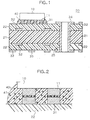
- FIG. 1 shows an example in which a semiconductor chip is bonded to a mounting substrate by means of an adhesive not containing any conductive particles.
- Fig. 2 shows a bonded portion where a semiconductor chip is bonded to a mounting substrate by means of an adhesive containing conductive particles.
- FIG. 1 An electronic component device shown in Fig. 1 is constituted of a mounting substrate 20 and a semiconductor chip 10 mounted thereon. Incidentally, Fig. 1 shows part of the electronic component device. Actually, other component parts such as other semiconductor chips are mounted on the mounting substrate 20.
- projected electrodes (bumps) serving as connecting electrodes 11 are formed on its one face.
- the chip is electrically interconnected to the mounting substrate via the connecting electrodes 11.
- the mounting substrate 20 has a plurality of insulating layers 21 and 22, a plurality of wiring layers 32 and 33 disposed via the insulating layers 21 and 22, connecting electrode terminals 31 for making connection with the connecting electrodes 11 of the semiconductor chip 10, and a conductor 34 provided through the insulating layers 21 and 22 to electrically interconnect wiring layers specified among the wiring layers 32 and 33.
- the insulating layers 21 and 22 are provided, at their necessary spots, with holes 25 for serving as through-holes. More specifically, this mounting substrate constitutes a resin composite type multi-layer wiring board.
- the wiring layers 32 are provided as an inner-layer circuit
- the wiring layers 33 are provided as an outer-layer circuit.
- the connecting electrode terminals 31 function as a conductor circuit on which the chip is to be mounted.
- the projected electrodes (bumps) which are connecting electrodes 11 provided on the semiconductor chip 10 are registered on the connecting electrode terminals 31 provided on the surface of the mounting substrate 20.
- a film adhesive 40 for bonding has been disposed between the semiconductor chip 10 and the. mounting substrate 20. In this state, pressure and heat are applied from the part on the side of the semiconductor chip 10, whereby the adhesive 40 come to flow and then cure, so that the connecting electrodes 11 provided on the semiconductor chip 10 and the connecting electrode terminals 31 provided on the surface of the mounting substrate 20 come into direct mechanical contact to attain electrical interconnection.
- an adhesive 40 such as an anisotropic conductive adhesive having conductive particles 41
- the connecting electrodes 11 are connected to the connecting electrode terminals 31 in the state the conductive particles 41 are interposed between them, and simultaneously bonded and fixed there.
- the anisotropic conductive adhesive 40 is used and in the state where electrode surfaces facing each other to be bonded are brought into pressure contact, the conduction between the electrodes facing each other is effected via the conductive particles interposed between them.
- the adhesive though containing conductive particles, has the conductive particles in a low density and hence exhibits no conductivity.
- the mounting substrate 20 has at least one first insulating layer 21 formed of a resin reinforced with a glass base material, and a second insulating layer 22 which constitutes one layer at least on the side on which the electronic component parts are bonded and fixed.
- the second insulating layer 22 is also provided on the side different from the side on which the electronic component parts are bonded and fixed.
- any stress at the interface between the semiconductor chip and the adhesive for bonding circuit members can be relaxed, and besides, in the case when it has a modulus of elasticity of from 30 to 2,000 MPa at 40°C as the adhesive resin composition, the stress generated in reliability tests such as the thermal shock test, PCT or solder bath immersion test can also be absorbed by the adhesive resin composition.
- the adhesive may cause neither increase in connection resistance at bonded portions nor separation at adhesive layers even after the reliability tests, bringing about a great improvement in connection reliability.
- the present invention makes it possible to provide a gradation of physical properties in the thickness direction of the adhesive for bonding circuit members, and hence the adhesive can absorb internal stress generated in the reliability tests such as the thermal shock test, PCT or solder bath immersion test.
- the adhesive may cause neither increase in connection resistance at bonded portions nor separation at adhesive layers even after the reliability tests, bringing about a great improvement in connection reliability.
- the film adhesive is convenient to handle.
- the adhesive of the present invention may preferably be used to make electrical connection between LCD (liquid-crystal display) panels and TAB (tape automated bonding) substrates, TAB substrates and flexible circuit substrates, LCD panels and IC chips, and IC chips 'and printed wiring substrates only in the direction of pressing at the time of bonding.
- LCD liquid-crystal display
- TAB tape automated bonding
- the circuit board of the present invention can absorb the stress generated in the reliability tests, and may cause neither increase in connection resistance at bonded portions nor separation at adhesive layers even after the reliability tests, bringing about a great improvement in connection reliability.
- the film adhesive having a small coefficient of thermal expansion is used on the chip side and the stress generated at the interface between the chip and the adhesive can be relaxed.
- Fig. 1 is a cross-sectional illustration of an example of the construction of an electronic component device according to the present invention.
- Fig. 2 is a cross-sectional illustration of an example of the state of connection between electronic component parts and a mounting substrate.
- liquid epoxy epoxy equivalent weight: 185
- microcapsular latent curing agent a microcapsular latent curing agent
- fused silica average particle diameter: 0.5 ⁇ m
- nickel particles nickel particles
- This film coating fluid was coated on a separator (silicone-treated polyethylene terephthalate film; thickness: 40 ⁇ m) by means of a roll coater, followed by drying at 100°C for 10 minutes to form an adhesive film a of 45 ⁇ m thick.
- This adhesive film a had a modulus of elasticity at 40°C of 800 MPa after curing as measured with a dynamic viscoelasticity measuring instrument on only an adhesive resin composition from which the fused silica and nickel particles were removed.
- a chip (10 mm x 10 mm; thickness: 0.5 mm) with gold bumps (area: 80 ⁇ m x 80 ⁇ m each; space: 30 ⁇ m; height: 15 ⁇ m; the number of bumps: 288) was bonded to a Ni/Au-plated Cu circuit printed substrate in the manner as shown below.
- the adhesive film a (12 mm x 12 mm) was stuck to the Ni/Au-plated Cu circuit printed substrate (electrode height: 20 ⁇ m; thickness: 0.8 mm) at 80°C and 10 kgf/cm 2 . Thereafter, the separator was peeled, and the bumps of the chip were registered on the Ni/Au-plated Cu circuit printed substrate (thickness: 0.8 mm). Then, heat and pressure were applied from above the chip under conditions of 180°C, 30 g/bump and 20 seconds to effect main bonding.
- connection resistance after the main bonding was 6 m ⁇ at maximum per bump and 2 m ⁇ on the average, and insulation resistance was 10 8 ⁇ or above. These values did not change even after 1,000-cycle treatment in a thermal shock test made at -55 to 125°C, after a PCT (121°C, 2 atmospheric pressure) made for 200 hours, and after 260°C solder bath immersion for 10 seconds, showing good connection reliability.
- liquid epoxy epoxy equivalent weight: 185
- microcapsular latent curing agent a microcapsular latent curing agent
- fused silica average particle diameter: 0.5 ⁇ m
- nickel particles nickel particles
- This film coating fluid was coated on a separator (silicone-treated polyethylene terephthalate film; thickness: 40 ⁇ m) by means of a roll coater, followed by drying at 100°C for 10 minutes to form an adhesive film b of 45 ⁇ m thick.
- This adhesive film b had a modulus of elasticity at 40°C of 400 MPa after curing as measured with a dynamic viscoelasticity measuring instrument on only an adhesive resin composition from which the fused silica and nickel particles were removed.
- a chip (10 mm x 10 mm) with gold bumps (area: 80 ⁇ m x 80 ⁇ m each; space: 30 ⁇ m; height: 15 ⁇ m; the number of bumps: 288) was bonded to a Ni/Au-plated Cu circuit printed substrate (electrode height: 20 ⁇ m; thickness: 0.8 mm) in the manner as shown below.
- the adhesive film b (12 mm x 12 mm) was stuck to the Ni/Au-plated Cu circuit printed substrate at 80°C and 10 kgf/cm 2 . Thereafter, the separator was peeled, and the bumps of the chip were registered on the Ni/Au-plated Cu circuit printed substrate. Then, heat and pressure were applied from above the chip under conditions of 170°C, 30 g/bump and 20 seconds to effect main bonding.
- connection resistance after the main bonding was 18 m ⁇ at maximum per bump and 8 m ⁇ on the average, and insulation resistance was 10 8 ⁇ or above. These values did not change even after 1,000-cycle treatment in a thermal shock test made at -55 to 125°C, after a PCT (121°C, 2 atmospheric pressure) made for 200 hours, and after 260°C solder bath immersion for 10 seconds, showing good connection reliability.
- liquid epoxy epoxy equivalent weight: 185
- microcapsular latent curing agent a microcapsular latent curing agent
- fused silica average particle diameter: 0.5 ⁇ m
- conductive particles obtained by forming Au layers on polystyrene cores (diameter: 5 ⁇ m) were dispersed to obtain a film coating fluid.
- This film coating fluid was coated on a separator (silicone-treated polyethylene terephthalate film; thickness: 40 ⁇ m) by means of a roll coater, followed by drying at 100°C for 10 minutes to form an adhesive film c of 45 ⁇ m thick.
- This adhesive film c had a modulus of elasticity at 40°C of 1,000 MPa after curing as measured with a dynamic viscoelasticity measuring instrument on only an adhesive resin composition from which the fused silica and nickel particles were removed.
- a chip (10 mm x 10 mm; thickness: 0.5 mm) with gold bumps (area: 80 ⁇ m x 80 ⁇ m each; space: 30 ⁇ m; height: 15 ⁇ m; the number of bumps: 288) was bonded to a Ni/Au-plated Cu circuit printed substrate (electrode height: 20 ⁇ m; thickness: 0.8 mm) in the manner as shown below.
- the adhesive film c (12 mm x 12 mm) was stuck to the Ni/Au-plated Cu circuit printed substrate at 80°C and 10 kgf/cm 2 . Thereafter, the separator was peeled, and the bumps of the chip were registered on the Ni/Au-plated Cu circuit printed substrate. Then, heat and pressure were applied from above the chip under conditions of 170°C, 30 g/bump and 20 seconds to effect main bonding.
- connection resistance after the main bonding was 5 m ⁇ at maximum per bump and 1.5 m ⁇ on the average, and insulation resistance was 10 8 ⁇ or above. These values did not change even after 1,000-cycle treatment in a thermal shock test made at -55 to 125°C, after a PCT (121°C, 2 atmospheric pressure) made for 200 hours, and after 260°C solder bath immersion for 10 seconds, showing good connection reliability.
- liquid epoxy epoxy equivalent weight: 185
- microcapsular latent curing agent a microcapsular latent curing agent
- fused silica average particle diameter: 0.5 ⁇ m
- conductive particles obtained by forming Au layers on polystyrene cores (diameter: 5 ⁇ m) were dispersed to obtain a film coating fluid.
- This film coating fluid was coated on a separator (silicone-treated polyethylene terephthalate film; thickness: 40 ⁇ m) by means of a roll coater, followed by drying at 100°C for 10 minutes to form an adhesive film d of 45 ⁇ m thick.
- This adhesive film d had a modulus of elasticity at 40°C of 1,000 MPa after curing as measured with a dynamic viscoelasticity measuring instrument on only an adhesive resin composition from which the fused silica and nickel particles were removed.
- the adhesive film d had an average coefficient of thermal expansion at 110 to 130°C of 111 ppm as measured by the TMA method.
- a chip (1.7 mm x 17 mm; thickness: 0.5 mm) with gold bumps (area: 50 ⁇ m x 50 ⁇ m each; 362 bumps; space: 20 ⁇ m; height: 15 ⁇ m) was bonded to a glass substrate (thickness: 1.1 mm) with an ITO (yttrium tin oxide) circuit in the manner as shown below.
- ITO yttrium tin oxide
- the adhesive film c (12 mm x 12 mm) was stuck to the glass substrate with an ITO circuit at 80°C and 10 kgf/cm 2 . Thereafter, the separator was peeled, and the bumps of the chip were registered on the glass substrate with an ITO circuit. Then; heat and pressure were applied from above the chip under conditions of 180°C, 40 g/bump and 20 seconds to effect main bonding.
- connection resistance after the main bonding was 150 m ⁇ at maximum per bump and 80 m ⁇ on the average, and insulation resistance was 10 8 ⁇ or above. These values did not change even after 1,000-cycle treatment in a thermal shock test made at -40 to 100°C and after a PCT (105°C, 1.2 atmospheric pressure) made for 100 hours, showing good connection reliability.
- liquid epoxy epoxy equivalent weight: 185
- microcapsular latent curing agent a microcapsular latent curing agent
- fused silica average particle diameter: 0.5 ⁇ m
- nickel particles nickel particles
- This film coating fluid was coated on a separator (silicone-treated polyethylene terephthalate film; thickness: 40 ⁇ m) by means of a roll coater, followed by drying at 100°C for 10 minutes to form an adhesive film e of 45 ⁇ m thick.
- This adhesive film e had a modulus of elasticity at 40°C of 800 MPa after curing as measured with a dynamic viscoelasticity measuring instrument on only an adhesive resin composition from which the fused silica and nickel particles were removed.
- a bumpless chip (10 mm x 10 mm; thickness: 0.5 mm; pad electrode: Al; pad diameter: 120 ⁇ m
- a Ni/Au-plated Cu circuit printed substrate on the circuit of which Ni/Au-plated Cu bumps (diameter: 100 ⁇ m; space: 50 ⁇ m; height: 15 ⁇ m; the number of bumps: 200) were formed, which was bonded in the manner as shown below.
- the adhesive film e (12 mm x 12 mm) was stuck to the Ni/Au-plated Cu circuit printed substrate (electrode height: 20 ⁇ m; thickness: 0.8 mm) at 80°C and 10 kgf/cm 2 . Thereafter, the separator was peeled, and the Al pads of the chip were registered on the Ni/Au-plated Cu circuit printed substrate (thickness: 0.8 mm) with Ni/Au-plated Cu bumps. Then, heat and pressure were applied from above the chip under conditions of 180°C, 30 g/bump and 20 seconds to effect main bonding.
- connection resistance after the main bonding was 8 m ⁇ at maximum per bump and 4 m ⁇ on the average, and insulation resistance was 10 8 ⁇ or above. These values did not change even after 1,000-cycle treatment in a thermal shock test made at -55 to 125°C, after a PCT (121°C, 2 atmospheric pressure) made for 200 hours, and after 260°C solder bath immersion for 10 seconds, showing good connection reliability.
- liquid epoxy epoxy equivalent weight: 185
- fused silica average particle diameter: 0.5 ⁇ m
- This film coating fluid was coated on a separator (silicone-treated polyethylene terephthalate film; thickness: 40 ⁇ m) by means of a roll coater, followed by drying at 100°C for 10 minutes to form a first adhesive layer, adhesive film f (thickness: 25 ⁇ m).
- This adhesive film f had a modulus of elasticity at 40°C of 800 MPa after curing as measured with a dynamic viscoelasticity measuring instrument on only an adhesive resin composition from which the fused silica was removed.
- a second adhesive layer, adhesive film g (thickness: 25 ⁇ m) was also formed in the same manner as the formation of the adhesive film g except that 2% by volume of nickel particles (diameter: 3 ⁇ m) were dispersed in place of the dispersing of the fused silica.
- the resultant adhesive film g had a modulus of elasticity at 40°C of 800 MPa.
- a chip (10 mm x +10 mm; thickness: 0.5 mm) with gold bumps (area: 80 ⁇ m x 80 ⁇ m each; space: 30 ⁇ m; height: 15 ⁇ m; the number of bumps: 288) was bonded to a Ni/Au-plated Cu circuit printed substrate in the manner as shown below.
- the adhesive film g (second adhesive layer) of this laminated film adhesive h (12 mm x 12 mm) was stuck to the Ni/Au-plated Cu circuit printed substrate (electrode height: 20 ⁇ m; thickness: 0.8 mm) at 80°C and 10 kgf/cm 2 . Thereafter, the separator was peeled, and the chip was faced on the side of the adhesive film f (first adhesive layer), where the bumps of the chip were registered on the Ni/Au-plated Cu circuit printed substrate (thickness: 0.8 mm). Then, heat and pressure were applied from above the chip under conditions of 180°C,. 50 g/bump and 20 seconds to effect main bonding.
- connection resistance after the main bonding was 6 m ⁇ at maximum per bump and 2 m ⁇ on the average, and insulation resistance was 10 8 ⁇ or above. These values did not change even after 1,000-cycle treatment in a thermal shock test made at -55 to 125°C, after a PCT (121°C, 2 atmospheric pressure) made for 200 hours, and after 260°C solder bath immersion for 10 seconds, showing good connection reliability.
- This film coating fluid was coated on a separator (silicone-treated polyethylene terephthalate film; thickness: 40 ⁇ m) by means of a roll coater, followed by drying at 100°C for 10 minutes to form an adhesive film i (thickness: 20 ⁇ m) corresponding to the first adhesive layer.
- This adhesive film i had a modulus of elasticity at 40°C of 400 MPa after curing as measured with a dynamic viscoelasticity measuring instrument on only an adhesive resin composition from which the fused silica was removed.
- An adhesive film j (thickness: 20 ⁇ m) corresponding to the second adhesive layer was also formed in the same manner as the formation of the adhesive film i except that 2% by volume of nickel particles (diameter: 5 ⁇ m) were dispersed in place of the dispersing of the fused silica.
- the resultant adhesive film j had a modulus of elasticity at 40 °C of 400 MPa.
- the adhesive film i and adhesive film j thus obtained were laminated to obtain a composite film, laminated film adhesive k.
- a chip (10 mm x 10 mm; thickness: 0.5 mm) with gold bumps (area: 80 ⁇ m x 80 ⁇ m each; space: 30 ⁇ m; height: 15 ⁇ m; the number of bumps: 288) was bonded to a Ni/Au-plated Cu circuit printed substrate in the manner as shown below.
- the adhesive film j (second adhesive layer) of this laminated film adhesive k (12 mm x 12 mm) was stuck to the Ni/Au-plated Cu circuit printed substrate (electrode height: 20 ⁇ m; thickness: 0.8 mm) at 80°C and 10 kgf/cm 2 . Thereafter, the separator was peeled, and the chip was faced on the side of the adhesive film i (first adhesive layer), where the bumps of the chip were registered on the Ni/Au-plated Cu circuit printed substrate (thickness: 0.8 mm). Then, heat and pressure were applied from above the chip under conditions of 180°C, 50 g/bump and 20 seconds to effect main bonding.
- connection resistance after the main bonding was 18 m ⁇ at maximum per bump and 8 m ⁇ on the average, and insulation resistance was 10 8 ⁇ or above. These values did not change even after 1,000-cycle treatment in a thermal shock test made at -55 to 125°C, after a PCT (121°C, 2 atmospheric pressure) made for 200 hours, and after 260°C solder bath immersion for 10 seconds, showing good connection reliability.
- liquid epoxy epoxy equivalent weight: 185
- fused silica average particle diameter: 0.5 ⁇ m
- This film coating fluid was coated on a separator (silicone-treated polyethylene terephthalate film; thickness: 40 ⁇ m) by means of a roll coater, followed by drying at 100°C for 10 minutes to form an adhesive film m (thickness: 25 ⁇ m) corresponding to the first adhesive layer.
- This adhesive film m had a modulus of elasticity at 40°C of 1,000 MPa after curing as measured with a dynamic viscoelasticity measuring instrument on only an adhesive resin composition from which the fused silica was removed.
- An adhesive film n (thickness: 25 ⁇ m) corresponding to the second adhesive layer was also formed in the same manner as the formation of the adhesive film m except that 5% by volume of conductive particles obtained by forming Au layers on polystyrene cores (diameter: 5 ⁇ m) were dispersed in place of the dispersing of the fused silica.
- the resultant adhesive film n had a modulus of elasticity at 40 °C of 1,000 MPa.
- the adhesive film m and adhesive film n thus obtained were laminated to obtain a composite film, laminated film adhesive p.
- a chip (10 mm x 10 mm; thickness: 0.5 mm) with gold bumps (area: 80 ⁇ m x 80 ⁇ m each; space: 30 ⁇ m; height: 15 ⁇ m; the number of bumps: 288) was bonded to a Ni/Au-plated Cu circuit printed substrate in the manner as shown below.
- the adhesive film n (second adhesive layer) of this laminated film adhesive p (12 mm x 12 mm) was stuck to the Ni/Au-plated Cu circuit printed substrate (electrode height: 20 ⁇ m; thickness: 0.8 mm) at 80°C and 10 kgf/cm 2 . Thereafter, the separator was peeled, and the chip was faced on the side of the adhesive film m (first adhesive layer), where the bumps of the chip were registered on the Ni/Au-plated Cu circuit printed substrate (thickness: 0.8 mm). Then, heat and pressure were applied from above the chip under conditions of 180°C, 50 g/bump and 20 seconds to effect main bonding.
- connection resistance after the main bonding was 5 m ⁇ at maximum per bump and 1.5 m ⁇ on the average, and insulation resistance was 10 8 ⁇ or above. These values did not change even after 1,000-cycle treatment in a thermal shock test made at -55 to 125°C, after a PCT (121°C, 2 atmospheric pressure) made for 200 hours, and after 260°C solder bath immersion for 10 seconds, showing good connection reliability.
- liquid epoxy epoxy equivalent weight: 185
- fused silica average particle diameter: 0.5 ⁇ m
- This film coating fluid was coated on a separator (silicone-treated polyethylene terephthalate film; thickness: 25 ⁇ m) by means of a roll coater, followed by drying at 100°C for 10 minutes to form an adhesive film q (thickness: 25 ⁇ m) corresponding to the first adhesive layer.
- This adhesive film q had a modulus of elasticity at 40°C of 800 Mpa after curing as measured with a dynamic viscoelasticity measuring instrument on only an adhesive resin composition from which the fused silica was removed.
- An adhesive film r (thickness: 25 ⁇ m) corresponding to the second adhesive layer was also formed in the same manner as the formation of the adhesive film q except that 2% by volume of nickel particles (diameter: 3 ⁇ m) were dispersed in place of the dispersing of the fused silica.
- the resultant adhesive film r had a modulus of elasticity at 40°C of 800 MPa.
- a bumpless chip (10 mm x 10 mm; thickness: 0.5 mm; pad electrode: Al; pad diameter: 120 ⁇ m
- a Ni/Au-plated Cu circuit printed substrate on the circuit of which Ni/Au-plated Cu bumps (diameter: 100 ⁇ m; space: 50 ⁇ m; height: 15 ⁇ m; the number of bumps: 200) were formed, which was bonded in the manner as shown below.
- the adhesive film r (second adhesive layer) of this laminated film adhesive s (12 mm x 12 mm) was stuck at 80°C and 10 kgf/cm 2 , to the Ni/Au-plated Cu circuit printed substrate on which Ni/Au-plated Cu bumps (diameter: 100 ⁇ m; space: 50 ⁇ m; height: 15 ⁇ m; the number of bumps: 200) were formed. Thereafter, the separator was peeled, and the chip was faced on the side of the adhesive film q (first adhesive layer), where the bumps of the chip were registered on the Ni/Au-plated Cu circuit printed substrate (thickness: 0.8 mm). Then, heat and pressure were applied from above the chip under conditions of 180°C, 50 g/bump and 20 seconds to effect main bonding.
- connection resistance after the main bonding was 8 m ⁇ at maximum per bump and 4 m ⁇ on the average, and insulation resistance was 10 8 ⁇ or above. These values did not change even after 1,000-cycle treatment in a thermal shock test made at -55 to 125°C, after a PCT (121°C, 2 atmospheric pressure) made for 200 hours, and after 260°C solder bath immersion for 10 seconds, showing good connection reliability.
- This film coating fluid was coated on a separator (silicone-treated polyethylene terephthalate film; thickness: 40 ⁇ m) by means of a roll coater, followed by drying at 100°C for 10 minutes to form an adhesive film t (thickness: 25 ⁇ m) corresponding to the third adhesive layer.
- This adhesive film t had a coefficient of thermal expansion of 45 ppm at 30 to 100°C after curing, a glass transition temperature of 150°C and a modulus of elasticity at 40°C of 2,600 MPa.
- This film coating fluid was coated on a separator (silicone-treated polyethylene terephthalate film; thickness: 40 ⁇ m) by means of a roll coater, followed by drying at 100°C for 10 minutes to form an adhesive film u (thickness: 25 ⁇ m) corresponding to the fourth adhesive layer.
- This adhesive film u had a coefficient of thermal expansion of 70 ppm at 30 to 100°C after curing, a glass transition temperature of 125°C and a modulus of elasticity at 40°C of 1,000 MPa.
- a chip (size: 10 mm x 10 mm; thickness: 0.55 mm) with gold bumps (height: 30 ⁇ m; the number of bumps: 184) was bonded to a Ni/Au-plated Cu circuit printed substrate (electrode height: 20 ⁇ m; substrate thickness: 0.8 mm) in the manner as shown below.
- the adhesive film u (fourth adhesive layer) of this laminated film adhesive v (size: 12 mm x 12 mm) was provisionally bonded to the Ni/Au-plated Cu circuit printed substrate with the adhesive film u's face set on the side of the printed substrate, under conditions of 60°C and 0.5 MPa.
- the bumps of the chip were registered on the Ni/Au-plated Cu circuit printed substrate, and the chip was mounted on the laminated film adhesive v. Subsequently, heat and pressure were applied from above the chip under conditions of 180°C, 50 g/bump and 20 seconds to effect main bonding.
- connection resistance after the main bonding was 10 m ⁇ at maximum per bump and 2 m ⁇ on the average, and insulation resistance was 10 8 ⁇ or above. These values did not change. during continuous (in situ) measurement of resistance in the course of a 1,000-cycle thermal shock test made at -55 to 125°C and a PCT made for 500 hours at 110°C and 85%RH, showing a good connection reliability.
- liquid epoxy epoxy equivalent weight: 185
- microcapsular latent curing agent a microcapsular latent curing agent
- fused silica average particle diameter: 0.5 ⁇ m
- nickel particles nickel particles
- This film coating fluid was coated on a separator (silicone-treated polyethylene terephthalate film; thickness: 40 ⁇ m) by means of a roll coater, followed by drying at 100°C for 10 minutes to form an adhesive film w (thickness: 25 ⁇ m) corresponding to the third adhesive layer.
- This adhesive film w had a coefficient of thermal expansion of 38 ppm at 30 to 100°C after curing, a glass transition temperature of 153°C and a modulus of elasticity at 40°C of 3,000 MPa.
- liquid epoxy epoxy equivalent weight: 185
- microcapsular latent curing agent a microcapsular latent curing agent
- fused silica average particle diameter: 0.5 ⁇ m
- nickel particles nickel particles
- This film coating fluid was coated on a separator (silicone-treated polyethylene terephthalate film; thickness: 40 ⁇ m) by means of a roll coater, followed by drying at 100°C for 10 minutes to form an adhesive film x (thickness: 25 ⁇ m) corresponding to the fourth adhesive layer.
- This adhesive film x had a coefficient of thermal expansion of 60 ppm at 30 to 100°C after curing, a glass transition temperature of 127°C and a modulus of elasticity at 40°C of 1,400 MPa.
- a chip (size: 10 mm x 10 mm; thickness: 0.55 mm) with gold bumps (height: 30 ⁇ m; the number of bumps: 184) was bonded to a Ni/Au-plated Cu circuit printed substrate (electrode height: 20 ⁇ m; substrate thickness: 0.8 mm) in the manner as shown below.
- the adhesive film x (fourth adhesive layer) of this laminated film adhesive y (size: 12 mm x 12 mm) was provisionally bonded to the Ni/Au-plated Cu circuit printed substrate with the adhesive film x's face set on the side of the printed substrate, under conditions of 60°C and 0.5 MPa. After the step of provisional bonding, the bumps of the chip were registered on the Ni/Au-plated Cu circuit printed substrate, and the chip was mounted on the laminated film adhesive y. Subsequently, heat and pressure were applied from above the chip under conditions of 180°C, 50 g/bump and 20 seconds to effect main bonding.
- Connection resistance after the main bonding was 10 m ⁇ at maximum per bump and 2 m ⁇ on the average, and insulation resistance was 10 8 ⁇ or above. These values did not change during continuous (in situ) measurement of resistance in the course of a 1,000-cycle thermal shock test made at -55 to 125°C and a PCT made for 500 hours at 110°C and 85%RH, showing good connection reliability.
- Example 10 Using the laminated film adhesive v obtained in Example 10, a chip (size: 10 mm x 10 mm; thickness: 0.55 mm) with gold bumps (height: 30 ⁇ m; the number of bumps: 184) was bonded to a Ni/Au-plated Cu circuit printed substrate (electrode height: 20 ⁇ m; substrate thickness: 0.8 mm) in the same manner as in Example 10 except that, in the present Comparative Example, the face of the adhesive film t (third adhesive layer) of the laminated film adhesive v (size: 12 mm x 12 mm) was set on the side of the printed substrate.
- connection resistance after the main bonding was 10 m ⁇ at maximum per bump and 2 m ⁇ on the average, and insulation resistance was 10 8 ⁇ or above.
- these values changed in the course of a 500-cycle thermal shock test made at -55 to 125°C and a PCT made for 300 hours at 110°C and 85%RH, resulting in faulty electrical conduction.
- This film coating fluid was coated on a separator (silicone-treated polyethylene terephthalate film; thickness: 40 ⁇ m) by means of a roll coater, followed by drying at 100°C for 10 minutes to form an adhesive film z of 50 ⁇ m thick.
- the adhesive film z had a coefficient of thermal expansion of 45 ppm at 30 to 100°C after curing, a glass transition temperature of 150°C and a modulus of elasticity at 40°C of 2,600 MPa.
- a chip (size: 10 mm x 10 mm; thickness: 0.55 mm) with gold bumps (height: 30 ⁇ m; the number of bumps: 184) was bonded to a Ni/Au-plated Cu circuit printed substrate (electrode height: 20 ⁇ m; substrate thickness: 0.8 mm) in the manner as shown below.
- the adhesive film z was provisionally bonded to the Ni/Au-plated Cu circuit printed substrate under conditions of 60°C and 0.5 MPa. After the step of provisional bonding, the bumps of the chip were registered on the Ni/Au-plated Cu circuit printed substrate, and the chip was mounted on the adhesive film z. Subsequently, heat and pressure were applied from above the chip under conditions of 180°C, 50 g/bump and 20 seconds to effect main bonding.
- connection resistance after the main bonding was 10 m ⁇ at maximum per bump and 3 m ⁇ on the average, and insulation resistance was 10 8 ⁇ or above.
- these values changed after a 300-cycle thermal shock test made at -55 to 125°C and after 260°C solder bath immersion for 10 seconds, resulting in faulty electrical conduction.
- separation of the adhesive film at its interface was observed at some part where the faulty electrical conduction occurred.
- This film coating fluid was coated on a separator (silicone-treated polyethylene terephthalate film; thickness: 40 ⁇ m) by means of a roll coater, followed by drying at 100°C for 10 minutes to form an adhesive film ⁇ of 25 ⁇ m thick.
- This adhesive film ⁇ had a coefficient of thermal expansion of 60 ppm at 30 to 100°C after curing, a glass transition temperature of 125°C and a modulus of elasticity at 40°C of 1,000 MPa.
- a chip (size: 10 mm x 10 mm; thickness: 0.55 mm) with gold bumps (height: 30 ⁇ m; the number of bumps: 184) was bonded to a Ni/Au-plated Cu circuit printed substrate (electrode height: 20 ⁇ m; substrate thickness: 0.8 mm) in the manner as shown below.
- the adhesive film ⁇ was provisionally bonded to the Ni/Au-plated Cu circuit printed substrate under conditions of 60°C and 0.5 MPa. After the step of provisional bonding, the bumps of the chip were registered on the Ni/Au-plated Cu circuit printed substrate, and the chip was mounted on the adhesive film ⁇ . Subsequently, heat and pressure were applied from above the chip under conditions of 180°C, 50 g/bump and 20 seconds to effect main bonding.
- connection resistance after the main bonding was 10 m ⁇ at maximum per bump and 2 m ⁇ on the average, and insulation resistance was 10 8 ⁇ or above.
- these values changed during a high-temperature thermal shock test in a 30-cycle thermal shock test made at -55 to 125°C, so that the electrical conduction became poor.
- the present invention enables production of circuit boards that may cause neither increase in connection resistance at bonded portions nor separation at adhesive layers and have greatly improved in connection reliability.
Landscapes
- Chemical & Material Sciences (AREA)
- Engineering & Computer Science (AREA)
- Organic Chemistry (AREA)
- Microelectronics & Electronic Packaging (AREA)
- Manufacturing & Machinery (AREA)
- Health & Medical Sciences (AREA)
- Inorganic Chemistry (AREA)
- Chemical Kinetics & Catalysis (AREA)
- Medicinal Chemistry (AREA)
- Polymers & Plastics (AREA)
- Adhesives Or Adhesive Processes (AREA)
- Adhesive Tapes (AREA)
- Wire Bonding (AREA)
Priority Applications (1)
| Application Number | Priority Date | Filing Date | Title |
|---|---|---|---|
| EP04013449A EP1454973B1 (de) | 1998-08-13 | 1998-08-13 | Klebstoff zum Verbinden von Schaltelementen, Leiterplatten und Verfahren zur Herstellung derselben |
Applications Claiming Priority (1)
| Application Number | Priority Date | Filing Date | Title |
|---|---|---|---|
| PCT/JP1998/003609 WO2000009623A1 (fr) | 1998-08-13 | 1998-08-13 | Adhesif pour fixer des elements de circuit, carte de circuit imprime et procede de production |
Related Child Applications (1)
| Application Number | Title | Priority Date | Filing Date |
|---|---|---|---|
| EP04013449A Division EP1454973B1 (de) | 1998-08-13 | 1998-08-13 | Klebstoff zum Verbinden von Schaltelementen, Leiterplatten und Verfahren zur Herstellung derselben |
Publications (3)
| Publication Number | Publication Date |
|---|---|
| EP1120449A1 true EP1120449A1 (de) | 2001-08-01 |
| EP1120449A4 EP1120449A4 (de) | 2002-10-23 |
| EP1120449B1 EP1120449B1 (de) | 2005-06-15 |
Family
ID=14208799
Family Applications (1)
| Application Number | Title | Priority Date | Filing Date |
|---|---|---|---|
| EP98937808A Expired - Lifetime EP1120449B1 (de) | 1998-08-13 | 1998-08-13 | Klebstoff zum verbinden von schaltelementen, leiterplatte und verfahren zur herstellung derselben |
Country Status (7)
| Country | Link |
|---|---|
| US (6) | US7247381B1 (de) |
| EP (1) | EP1120449B1 (de) |
| KR (1) | KR100388770B1 (de) |
| CN (2) | CN100379832C (de) |
| AU (1) | AU8648598A (de) |
| DE (1) | DE69830623T2 (de) |
| WO (1) | WO2000009623A1 (de) |
Cited By (7)
| Publication number | Priority date | Publication date | Assignee | Title |
|---|---|---|---|---|
| EP1454973A1 (de) * | 1998-08-13 | 2004-09-08 | Hitachi Chemical Co., Ltd. | Klebstoff zum Verbinden von Schaltelementen, Leiterplatten und Verfahren zur Herstellung derselben |
| KR100736890B1 (ko) | 2005-07-26 | 2007-07-06 | 새한미디어주식회사 | 이방성 도전 필름, 및 그 제조방법 |
| US7247381B1 (en) | 1998-08-13 | 2007-07-24 | Hitachi Chemical Company, Ltd. | Adhesive for bonding circuit members, circuit board, and method of producing the same |
| EP1832615A3 (de) * | 2006-03-10 | 2011-12-07 | Henkel AG & Co. KGaA | Klebstoffzusammensetzung |
| CN102543809A (zh) * | 2007-11-08 | 2012-07-04 | 日立化成工业株式会社 | 半导体芯片搭载方法 |
| EP2302013A4 (de) * | 2008-07-16 | 2013-07-17 | Sony Chem & Inf Device Corp | Anisotropes und leitfähiges haftmittel |
| EP2524953A4 (de) * | 2010-01-15 | 2015-08-12 | Dexerials Corp | Anisotropes, elektrisch leitfähiges haftmittel |
Families Citing this family (38)
| Publication number | Priority date | Publication date | Assignee | Title |
|---|---|---|---|---|
| CN1214455C (zh) * | 2000-04-25 | 2005-08-10 | 日立化成工业株式会社 | 电路连接用粘接剂、使用其的电路连接方法及电路连接结构体 |
| JP2002226808A (ja) * | 2001-01-31 | 2002-08-14 | Hitachi Chem Co Ltd | 回路接続用接着剤 |
| JP5274744B2 (ja) * | 2002-09-30 | 2013-08-28 | 日立化成株式会社 | フィルム状接着剤及びこれを用いた半導体装置 |
| JP4725704B2 (ja) * | 2003-05-27 | 2011-07-13 | 味の素株式会社 | 多層プリント配線板の層間絶縁用樹脂組成物、接着フィルム及びプリプレグ |
| TWI335347B (en) * | 2003-05-27 | 2011-01-01 | Ajinomoto Kk | Resin composition for interlayer insulation of multilayer printed wiring board, adhesive film and prepreg |
| KR20060026130A (ko) | 2004-09-18 | 2006-03-23 | 삼성전기주식회사 | 칩패키지를 실장한 인쇄회로기판 및 그 제조방법 |
| JP3852858B1 (ja) * | 2005-08-16 | 2006-12-06 | 株式会社日立製作所 | 半導体放射線検出器、放射線検出モジュールおよび核医学診断装置 |
| JP2007091959A (ja) * | 2005-09-30 | 2007-04-12 | Sumitomo Electric Ind Ltd | 異方導電性接着剤 |
| CA2637812C (en) * | 2006-04-20 | 2015-02-24 | Sumitomo Bakelite Co., Ltd. | Semiconductor device |
| US20100243303A1 (en) * | 2006-08-22 | 2010-09-30 | Hitachi Chemical Company, Ltd. | Circuit connecting material, connection structure of circuit member, and method for manufacturing connection structure of circuit member |
| TW200906263A (en) * | 2007-05-29 | 2009-02-01 | Matsushita Electric Industrial Co Ltd | Circuit board and method for manufacturing the same |
| US8040685B2 (en) | 2007-07-17 | 2011-10-18 | Ibiden Co., Ltd. | Stacked wiring board and method of manufacturing stacked wiring board |
| EP2180772A4 (de) * | 2007-08-24 | 2013-08-28 | Sumitomo Bakelite Co | Mehrschichtige leiterplatte und halbleiteranordnung |
| JP2009170753A (ja) * | 2008-01-18 | 2009-07-30 | Panasonic Corp | 多層プリント配線板とこれを用いた実装体 |
| DE102008015378A1 (de) * | 2008-03-20 | 2009-09-24 | Fraunhofer-Gesellschaft zur Förderung der angewandten Forschung e.V. | Anschlussstift und elektrischer Anschluss |
| JP5151902B2 (ja) * | 2008-10-21 | 2013-02-27 | 住友電気工業株式会社 | 異方導電性フィルム |
| JP5558140B2 (ja) | 2009-06-10 | 2014-07-23 | デクセリアルズ株式会社 | 絶縁性樹脂フィルム、並びにこれを用いた接合体及びその製造方法 |
| KR101025620B1 (ko) * | 2009-07-13 | 2011-03-30 | 한국과학기술원 | 초음파 접합용 이방성 전도성 접착제 및 이를 이용한 전자부품 간 접속방법 |
| JP5293779B2 (ja) * | 2010-07-20 | 2013-09-18 | 日立化成株式会社 | 接着剤組成物、回路接続構造体、半導体装置及び太陽電池モジュール |
| KR101719636B1 (ko) * | 2011-01-28 | 2017-04-05 | 삼성전자 주식회사 | 반도체 장치 및 그 제조 방법 |
| JP5387592B2 (ja) * | 2011-02-07 | 2014-01-15 | 日立化成株式会社 | 回路接続材料、及び回路部材の接続構造の製造方法 |
| JP5571045B2 (ja) * | 2011-08-19 | 2014-08-13 | 株式会社東芝 | 積層型半導体装置 |
| US20130070437A1 (en) * | 2011-09-20 | 2013-03-21 | Invensas Corp. | Hybrid interposer |
| JP5626179B2 (ja) * | 2011-10-24 | 2014-11-19 | 日立化成株式会社 | フィルム状接着剤及びこれを用いた半導体装置 |
| WO2013103282A1 (ko) * | 2012-01-06 | 2013-07-11 | 주식회사 엘지화학 | 봉지용 필름 |
| US20130256894A1 (en) * | 2012-03-29 | 2013-10-03 | International Rectifier Corporation | Porous Metallic Film as Die Attach and Interconnect |
| JP6425382B2 (ja) * | 2014-01-08 | 2018-11-21 | デクセリアルズ株式会社 | 接続方法、及び接合体 |
| US20150195912A1 (en) | 2014-01-08 | 2015-07-09 | Zhuhai Advanced Chip Carriers & Electronic Substrate Solutions Technologies Co. Ltd. | Substrates With Ultra Fine Pitch Flip Chip Bumps |
| DE102014210895A1 (de) * | 2014-06-06 | 2015-12-17 | Continental Automotive Gmbh | Mehrlagige Leiterplatte und Verfahren zu dessen Herstellung |
| TWI554174B (zh) | 2014-11-04 | 2016-10-11 | 上海兆芯集成電路有限公司 | 線路基板和半導體封裝結構 |
| US10064287B2 (en) * | 2014-11-05 | 2018-08-28 | Infineon Technologies Austria Ag | System and method of providing a semiconductor carrier and redistribution structure |
| US10192846B2 (en) | 2014-11-05 | 2019-01-29 | Infineon Technologies Austria Ag | Method of inserting an electronic component into a slot in a circuit board |
| US10553557B2 (en) | 2014-11-05 | 2020-02-04 | Infineon Technologies Austria Ag | Electronic component, system and method |
| JP6542526B2 (ja) * | 2014-11-12 | 2019-07-10 | デクセリアルズ株式会社 | 熱硬化性接着組成物、及び熱硬化性接着シート |
| KR101880053B1 (ko) * | 2017-04-26 | 2018-07-20 | (주)노피온 | 갭퍼를 포함하는 이방성 도전 접착제의 제조방법 및 갭퍼를 이용하는 부품 실장방법 |
| US10297564B2 (en) * | 2017-10-05 | 2019-05-21 | Infineon Technologies Ag | Semiconductor die attach system and method |
| CN109658831B (zh) * | 2018-12-20 | 2021-05-04 | 厦门天马微电子有限公司 | 一种显示面板及显示装置 |
| TW202341186A (zh) * | 2022-01-12 | 2023-10-16 | 日商力森諾科股份有限公司 | 接著劑組成物、電路連接用接著劑膜及連接結構體之製造方法 |
Family Cites Families (36)
| Publication number | Priority date | Publication date | Assignee | Title |
|---|---|---|---|---|
| JPS5121192A (ja) * | 1974-08-14 | 1976-02-20 | Seikosha Kk | Dodenseisetsuchakushiito |
| JPS58138740A (ja) | 1982-02-15 | 1983-08-17 | Denki Kagaku Kogyo Kk | 樹脂組成物 |
| JPS61215615A (ja) | 1985-03-22 | 1986-09-25 | Denki Kagaku Kogyo Kk | 半導体封止用樹脂組成物 |
| JPS6251111A (ja) * | 1985-08-29 | 1987-03-05 | 日東電工株式会社 | 異方導電性フイルム |
| JPH0623349B2 (ja) | 1986-01-30 | 1994-03-30 | 富士高分子工業株式会社 | 異方導電性接着剤 |
| JPH01236588A (ja) * | 1988-03-17 | 1989-09-21 | Matsushita Electric Ind Co Ltd | 異方導電性接着体 |
| JP2704281B2 (ja) | 1988-11-25 | 1998-01-26 | 日本化学工業株式会社 | 溶融球状シリカ及びこれをフィラーとする封止用樹脂組成物 |
| JPH02206670A (ja) | 1989-02-06 | 1990-08-16 | Hitachi Chem Co Ltd | 異方導電性を有する回路接続用熱伝導性接着剤組成物及び熱伝導性接着フィルム |
| JPH0384078A (ja) | 1989-08-29 | 1991-04-09 | Toray Ind Inc | 導電性接着剤 |
| JPH03223380A (ja) | 1990-01-30 | 1991-10-02 | Oki Electric Ind Co Ltd | 異方性導電接着剤 |
| JPH03234778A (ja) | 1990-02-08 | 1991-10-18 | Toray Ind Inc | 導電性接着剤 |
| JPH0733429B2 (ja) | 1990-04-04 | 1995-04-12 | 東レ株式会社 | エポキシ樹脂組成物 |
| JPH04118873A (ja) | 1990-09-08 | 1992-04-20 | Catalysts & Chem Ind Co Ltd | 異方導電性回路基材 |
| JP2740990B2 (ja) | 1991-11-26 | 1998-04-15 | 株式会社日立製作所 | 低熱膨張性加圧成形用樹脂組成物 |
| JP2830681B2 (ja) | 1993-03-08 | 1998-12-02 | ソニーケミカル株式会社 | Icチップ実装方法 |
| JP3103956B2 (ja) * | 1993-06-03 | 2000-10-30 | ソニーケミカル株式会社 | 異方性導電膜 |
| JPH0818818B2 (ja) | 1993-07-27 | 1996-02-28 | 科学技術庁無機材質研究所長 | Y−b系化合物とその製造方法 |
| JPH0766326A (ja) | 1993-08-30 | 1995-03-10 | Nippondenso Co Ltd | 半導体装置 |
| JPH07161764A (ja) | 1993-12-03 | 1995-06-23 | Toshiba Corp | 樹脂封止型半導体装置およびその製造方法 |
| JP3559817B2 (ja) * | 1994-06-16 | 2004-09-02 | 綜研化学株式会社 | 異方導電性接着剤および異方導電性接着シート |
| AU6015596A (en) | 1995-06-13 | 1997-01-09 | Hitachi Chemical Company, Ltd. | Semiconductor device, wiring board for mounting semiconducto r and method of production of semiconductor device |
| JP3084351B2 (ja) * | 1995-09-01 | 2000-09-04 | 住友ベークライト株式会社 | 多層プリント配線板用層間絶縁接着剤 |
| TW505686B (en) * | 1996-07-15 | 2002-10-11 | Hitachi Chemical Ltd | Film-like adhesive for connecting circuit and circuit board |
| US6034331A (en) * | 1996-07-23 | 2000-03-07 | Hitachi Chemical Company, Ltd. | Connection sheet and electrode connection structure for electrically interconnecting electrodes facing each other, and method using the connection sheet |
| KR100248582B1 (ko) * | 1996-07-30 | 2000-03-15 | 이사오 우치가사키 | 서로 마주보는 전극들을 상호 접속하기 위한 접속시트, 및 이 접속시트를 사용하는 전극접속구조 및 접속방법 |
| JP3928753B2 (ja) | 1996-08-06 | 2007-06-13 | 日立化成工業株式会社 | マルチチップ実装法、および接着剤付チップの製造方法 |
| EP0831528A3 (de) * | 1996-09-10 | 1999-12-22 | Hitachi Chemical Company, Ltd. | Mehrschicht-Leiterplatte zum Montieren einer Halbleiteranordnung und Herstellungsverfahren dafür |
| JPH10163254A (ja) * | 1996-12-03 | 1998-06-19 | Hitachi Chem Co Ltd | 回路板 |
| WO2000009623A1 (fr) | 1998-08-13 | 2000-02-24 | Hitachi Chemical Company, Ltd. | Adhesif pour fixer des elements de circuit, carte de circuit imprime et procede de production |
| JPH10226769A (ja) | 1997-02-17 | 1998-08-25 | Hitachi Chem Co Ltd | フィルム状接着剤及び接続方法 |
| JP4440352B2 (ja) | 1997-02-17 | 2010-03-24 | 日立化成工業株式会社 | 回路部材接続用接着剤 |
| JP4118873B2 (ja) | 2004-12-24 | 2008-07-16 | 有限会社 サンブレン | コンクリートの製造方法およびコンクリート製造の標準化システム |
| JP2007113012A (ja) | 2006-11-13 | 2007-05-10 | Hitachi Chem Co Ltd | 回路部材接続用接着剤 |
| JP4928378B2 (ja) | 2007-08-06 | 2012-05-09 | 日立化成工業株式会社 | 回路部材接続用接着剤 |
| JP4631979B2 (ja) | 2009-02-16 | 2011-02-16 | 日立化成工業株式会社 | 回路部材接続用接着剤並びに回路板及びその製造方法 |
| JP4631984B2 (ja) | 2009-07-03 | 2011-02-16 | 日立化成工業株式会社 | 回路部材接続用接着剤、回路板、及びその製造方法 |
-
1998
- 1998-08-13 WO PCT/JP1998/003609 patent/WO2000009623A1/ja not_active Ceased
- 1998-08-13 CN CNB2004100978881A patent/CN100379832C/zh not_active Expired - Fee Related
- 1998-08-13 KR KR10-2001-7001872A patent/KR100388770B1/ko not_active Expired - Lifetime
- 1998-08-13 EP EP98937808A patent/EP1120449B1/de not_active Expired - Lifetime
- 1998-08-13 US US09/762,823 patent/US7247381B1/en not_active Expired - Fee Related
- 1998-08-13 AU AU86485/98A patent/AU8648598A/en not_active Abandoned
- 1998-08-13 DE DE69830623T patent/DE69830623T2/de not_active Expired - Lifetime
- 1998-08-13 CN CNB988142716A patent/CN1230483C/zh not_active Expired - Fee Related
-
2007
- 2007-02-06 US US11/702,552 patent/US7879445B2/en not_active Expired - Fee Related
-
2009
- 2009-08-28 US US12/549,909 patent/US20090314533A1/en not_active Abandoned
-
2011
- 2011-06-22 US US13/166,577 patent/US8252419B2/en not_active Expired - Fee Related
- 2011-06-22 US US13/166,591 patent/US8273458B2/en not_active Expired - Fee Related
- 2011-06-22 US US13/166,570 patent/US8273457B2/en not_active Expired - Fee Related
Non-Patent Citations (2)
| Title |
|---|
| DATABASE WPI Section EI, Week 199917 Derwent Publications Ltd., London, GB; Class V04, AN 1999-202973 XP002210816 & KR 98 013 552 A (HITACHI CHEM CO LTD), 30 April 1998 (1998-04-30) * |
| See also references of WO0009623A1 * |
Cited By (15)
| Publication number | Priority date | Publication date | Assignee | Title |
|---|---|---|---|---|
| US8273458B2 (en) | 1997-02-14 | 2012-09-25 | Hitachi Chemical Company, Ltd. | Adhesive for bonding circuit members, circuit board and process for its production |
| US8252419B2 (en) | 1998-08-13 | 2012-08-28 | Hitachi Chemical Company, Ltd. | Adhesive for bonding circuit members, circuit board and process for its production |
| US7879445B2 (en) | 1998-08-13 | 2011-02-01 | Hitachi Chemical Company, Ltd. | Adhesive for bonding circuit members, circuit board and process for its production |
| US7247381B1 (en) | 1998-08-13 | 2007-07-24 | Hitachi Chemical Company, Ltd. | Adhesive for bonding circuit members, circuit board, and method of producing the same |
| EP1454973A1 (de) * | 1998-08-13 | 2004-09-08 | Hitachi Chemical Co., Ltd. | Klebstoff zum Verbinden von Schaltelementen, Leiterplatten und Verfahren zur Herstellung derselben |
| US8273457B2 (en) | 1998-08-13 | 2012-09-25 | Hitachi Chemical Company, Ltd. | Adhesive for bonding circuit members, circuit board and process for its production |
| KR100736890B1 (ko) | 2005-07-26 | 2007-07-06 | 새한미디어주식회사 | 이방성 도전 필름, 및 그 제조방법 |
| EP1832615A3 (de) * | 2006-03-10 | 2011-12-07 | Henkel AG & Co. KGaA | Klebstoffzusammensetzung |
| CN102543809A (zh) * | 2007-11-08 | 2012-07-04 | 日立化成工业株式会社 | 半导体芯片搭载方法 |
| CN102543809B (zh) * | 2007-11-08 | 2015-11-04 | 日立化成株式会社 | 半导体芯片搭载方法 |
| US9969909B2 (en) | 2007-11-08 | 2018-05-15 | Hitachi Chemical Company, Ltd. | Adhesive sheet for semiconductor, and dicing tape integrated adhesive sheet for semiconductor |
| EP2302013A4 (de) * | 2008-07-16 | 2013-07-17 | Sony Chem & Inf Device Corp | Anisotropes und leitfähiges haftmittel |
| US8636924B2 (en) | 2008-07-16 | 2014-01-28 | Dexerials Corporation | Anisotropic conductive adhesive |
| US9418958B2 (en) | 2008-07-16 | 2016-08-16 | Dexerials Corporation | Anisotropic conductive adhesive |
| EP2524953A4 (de) * | 2010-01-15 | 2015-08-12 | Dexerials Corp | Anisotropes, elektrisch leitfähiges haftmittel |
Also Published As
| Publication number | Publication date |
|---|---|
| KR20010106440A (ko) | 2001-11-29 |
| US7879445B2 (en) | 2011-02-01 |
| WO2000009623A1 (fr) | 2000-02-24 |
| US20110247867A1 (en) | 2011-10-13 |
| US20110247873A1 (en) | 2011-10-13 |
| US20110247874A1 (en) | 2011-10-13 |
| EP1120449B1 (de) | 2005-06-15 |
| DE69830623D1 (de) | 2005-07-21 |
| EP1120449A4 (de) | 2002-10-23 |
| US8273457B2 (en) | 2012-09-25 |
| CN1637105A (zh) | 2005-07-13 |
| AU8648598A (en) | 2000-03-06 |
| CN1322229A (zh) | 2001-11-14 |
| US8252419B2 (en) | 2012-08-28 |
| CN100379832C (zh) | 2008-04-09 |
| US7247381B1 (en) | 2007-07-24 |
| US20090314533A1 (en) | 2009-12-24 |
| CN1230483C (zh) | 2005-12-07 |
| US20070137887A1 (en) | 2007-06-21 |
| DE69830623T2 (de) | 2006-05-04 |
| KR100388770B1 (ko) | 2003-06-25 |
| US8273458B2 (en) | 2012-09-25 |
Similar Documents
| Publication | Publication Date | Title |
|---|---|---|
| US8273458B2 (en) | Adhesive for bonding circuit members, circuit board and process for its production | |
| US6328844B1 (en) | Filmy adhesive for connecting circuits and circuit board | |
| JP5581576B2 (ja) | フラックス活性剤、接着剤樹脂組成物、接着ペースト、接着フィルム、半導体装置の製造方法、及び半導体装置 | |
| JPWO1998003047A1 (ja) | 回路接続用フィルム状接着剤及び回路板 | |
| US6184577B1 (en) | Electronic component parts device | |
| JPH1150032A (ja) | 回路用接続部材及び回路板 | |
| JPH10289969A (ja) | 半導体装置およびそれに用いる封止用樹脂シート | |
| JP4631984B2 (ja) | 回路部材接続用接着剤、回路板、及びその製造方法 | |
| JP4631979B2 (ja) | 回路部材接続用接着剤並びに回路板及びその製造方法 | |
| JP3581618B2 (ja) | 導電性微粒子、異方性導電接着剤及び導電接続構造体 | |
| JP4631998B1 (ja) | 回路部材接続用接着剤、回路板、及びその製造方法 | |
| EP1454973B1 (de) | Klebstoff zum Verbinden von Schaltelementen, Leiterplatten und Verfahren zur Herstellung derselben | |
| JPH10273635A (ja) | 回路用接続部材及び回路板の製造法 | |
| CN1900195B (zh) | 电路构件连接用的粘结剂、电路板及其制造方法 | |
| JP3801341B2 (ja) | 電子部品装置 | |
| JP2001064619A (ja) | 回路接続用フィルム状接着剤 | |
| JPH11219980A (ja) | 電子部品装置 | |
| JP2007305994A (ja) | 回路用接続部材及び回路板 | |
| JP4385488B2 (ja) | 回路接続用フィルム状接着剤 | |
| JP3835583B2 (ja) | 電子部品装置 | |
| TW402631B (en) | An adhhesive for connecting circuit members, a circuit board and a method of manufacturing the circuit board | |
| JPWO2000009623A1 (ja) | 回路部材接続用接着剤並びに回路板及びその製造方法 | |
| JP3882967B2 (ja) | 回路板の製造法 | |
| JP2000003621A (ja) | 異方性導電膜及び導電接続構造体 |
Legal Events
| Date | Code | Title | Description |
|---|---|---|---|
| PUAI | Public reference made under article 153(3) epc to a published international application that has entered the european phase |
Free format text: ORIGINAL CODE: 0009012 |
|
| 17P | Request for examination filed |
Effective date: 20010306 |
|
| AK | Designated contracting states |
Kind code of ref document: A1 Designated state(s): DE FR GB NL |
|
| RIC1 | Information provided on ipc code assigned before grant |
Free format text: 7C 09J 9/00 A, 7C 09J 7/00 B |
|
| A4 | Supplementary search report drawn up and despatched |
Effective date: 20020905 |
|
| AK | Designated contracting states |
Kind code of ref document: A4 Designated state(s): DE FR GB NL |
|
| 17Q | First examination report despatched |
Effective date: 20030328 |
|
| GRAP | Despatch of communication of intention to grant a patent |
Free format text: ORIGINAL CODE: EPIDOSNIGR1 |
|
| GRAS | Grant fee paid |
Free format text: ORIGINAL CODE: EPIDOSNIGR3 |
|
| GRAA | (expected) grant |
Free format text: ORIGINAL CODE: 0009210 |
|
| AK | Designated contracting states |
Kind code of ref document: B1 Designated state(s): DE FR GB NL |
|
| REG | Reference to a national code |
Ref country code: GB Ref legal event code: FG4D |
|
| REF | Corresponds to: |
Ref document number: 69830623 Country of ref document: DE Date of ref document: 20050721 Kind code of ref document: P |
|
| ET | Fr: translation filed | ||
| PLBE | No opposition filed within time limit |
Free format text: ORIGINAL CODE: 0009261 |
|
| STAA | Information on the status of an ep patent application or granted ep patent |
Free format text: STATUS: NO OPPOSITION FILED WITHIN TIME LIMIT |
|
| 26N | No opposition filed |
Effective date: 20060316 |
|
| PGFP | Annual fee paid to national office [announced via postgrant information from national office to epo] |
Ref country code: FR Payment date: 20110818 Year of fee payment: 14 Ref country code: GB Payment date: 20110810 Year of fee payment: 14 |
|
| GBPC | Gb: european patent ceased through non-payment of renewal fee |
Effective date: 20120813 |
|
| REG | Reference to a national code |
Ref country code: FR Ref legal event code: ST Effective date: 20130430 |
|
| PG25 | Lapsed in a contracting state [announced via postgrant information from national office to epo] |
Ref country code: GB Free format text: LAPSE BECAUSE OF NON-PAYMENT OF DUE FEES Effective date: 20120813 |
|
| PG25 | Lapsed in a contracting state [announced via postgrant information from national office to epo] |
Ref country code: FR Free format text: LAPSE BECAUSE OF NON-PAYMENT OF DUE FEES Effective date: 20120831 |
|
| PGFP | Annual fee paid to national office [announced via postgrant information from national office to epo] |
Ref country code: NL Payment date: 20130815 Year of fee payment: 16 Ref country code: DE Payment date: 20130821 Year of fee payment: 16 |
|
| REG | Reference to a national code |
Ref country code: DE Ref legal event code: R119 Ref document number: 69830623 Country of ref document: DE |
|
| REG | Reference to a national code |
Ref country code: NL Ref legal event code: V1 Effective date: 20150301 |
|
| PG25 | Lapsed in a contracting state [announced via postgrant information from national office to epo] |
Ref country code: NL Free format text: LAPSE BECAUSE OF NON-PAYMENT OF DUE FEES Effective date: 20150301 |
|
| REG | Reference to a national code |
Ref country code: DE Ref legal event code: R119 Ref document number: 69830623 Country of ref document: DE Effective date: 20150303 |
|
| PG25 | Lapsed in a contracting state [announced via postgrant information from national office to epo] |
Ref country code: DE Free format text: LAPSE BECAUSE OF NON-PAYMENT OF DUE FEES Effective date: 20150303 |