EP1139155A2 - Appareil d'affichage à cristal liquide et son procédé de fabrication - Google Patents
Appareil d'affichage à cristal liquide et son procédé de fabrication Download PDFInfo
- Publication number
- EP1139155A2 EP1139155A2 EP01106688A EP01106688A EP1139155A2 EP 1139155 A2 EP1139155 A2 EP 1139155A2 EP 01106688 A EP01106688 A EP 01106688A EP 01106688 A EP01106688 A EP 01106688A EP 1139155 A2 EP1139155 A2 EP 1139155A2
- Authority
- EP
- European Patent Office
- Prior art keywords
- liquid crystal
- substrates
- crystal display
- display apparatus
- picture element
- Prior art date
- Legal status (The legal status is an assumption and is not a legal conclusion. Google has not performed a legal analysis and makes no representation as to the accuracy of the status listed.)
- Withdrawn
Links
Images

Classifications
-
- G—PHYSICS
- G02—OPTICS
- G02F—OPTICAL DEVICES OR ARRANGEMENTS FOR THE CONTROL OF LIGHT BY MODIFICATION OF THE OPTICAL PROPERTIES OF THE MEDIA OF THE ELEMENTS INVOLVED THEREIN; NON-LINEAR OPTICS; FREQUENCY-CHANGING OF LIGHT; OPTICAL LOGIC ELEMENTS; OPTICAL ANALOGUE/DIGITAL CONVERTERS
- G02F1/00—Devices or arrangements for the control of the intensity, colour, phase, polarisation or direction of light arriving from an independent light source, e.g. switching, gating or modulating; Non-linear optics
- G02F1/01—Devices or arrangements for the control of the intensity, colour, phase, polarisation or direction of light arriving from an independent light source, e.g. switching, gating or modulating; Non-linear optics for the control of the intensity, phase, polarisation or colour
- G02F1/13—Devices or arrangements for the control of the intensity, colour, phase, polarisation or direction of light arriving from an independent light source, e.g. switching, gating or modulating; Non-linear optics for the control of the intensity, phase, polarisation or colour based on liquid crystals, e.g. single liquid crystal display cells
- G02F1/133—Constructional arrangements; Operation of liquid crystal cells; Circuit arrangements
- G02F1/1333—Constructional arrangements; Manufacturing methods
- G02F1/1339—Gaskets; Spacers; Sealing of cells
-
- G—PHYSICS
- G02—OPTICS
- G02F—OPTICAL DEVICES OR ARRANGEMENTS FOR THE CONTROL OF LIGHT BY MODIFICATION OF THE OPTICAL PROPERTIES OF THE MEDIA OF THE ELEMENTS INVOLVED THEREIN; NON-LINEAR OPTICS; FREQUENCY-CHANGING OF LIGHT; OPTICAL LOGIC ELEMENTS; OPTICAL ANALOGUE/DIGITAL CONVERTERS
- G02F1/00—Devices or arrangements for the control of the intensity, colour, phase, polarisation or direction of light arriving from an independent light source, e.g. switching, gating or modulating; Non-linear optics
- G02F1/01—Devices or arrangements for the control of the intensity, colour, phase, polarisation or direction of light arriving from an independent light source, e.g. switching, gating or modulating; Non-linear optics for the control of the intensity, phase, polarisation or colour
- G02F1/13—Devices or arrangements for the control of the intensity, colour, phase, polarisation or direction of light arriving from an independent light source, e.g. switching, gating or modulating; Non-linear optics for the control of the intensity, phase, polarisation or colour based on liquid crystals, e.g. single liquid crystal display cells
- G02F1/133—Constructional arrangements; Operation of liquid crystal cells; Circuit arrangements
- G02F1/1333—Constructional arrangements; Manufacturing methods
- G02F1/1335—Structural association of cells with optical devices, e.g. polarisers or reflectors
- G02F1/133526—Lenses, e.g. microlenses or Fresnel lenses
-
- G—PHYSICS
- G02—OPTICS
- G02F—OPTICAL DEVICES OR ARRANGEMENTS FOR THE CONTROL OF LIGHT BY MODIFICATION OF THE OPTICAL PROPERTIES OF THE MEDIA OF THE ELEMENTS INVOLVED THEREIN; NON-LINEAR OPTICS; FREQUENCY-CHANGING OF LIGHT; OPTICAL LOGIC ELEMENTS; OPTICAL ANALOGUE/DIGITAL CONVERTERS
- G02F1/00—Devices or arrangements for the control of the intensity, colour, phase, polarisation or direction of light arriving from an independent light source, e.g. switching, gating or modulating; Non-linear optics
- G02F1/01—Devices or arrangements for the control of the intensity, colour, phase, polarisation or direction of light arriving from an independent light source, e.g. switching, gating or modulating; Non-linear optics for the control of the intensity, phase, polarisation or colour
- G02F1/13—Devices or arrangements for the control of the intensity, colour, phase, polarisation or direction of light arriving from an independent light source, e.g. switching, gating or modulating; Non-linear optics for the control of the intensity, phase, polarisation or colour based on liquid crystals, e.g. single liquid crystal display cells
- G02F1/133—Constructional arrangements; Operation of liquid crystal cells; Circuit arrangements
- G02F1/1333—Constructional arrangements; Manufacturing methods
- G02F1/1339—Gaskets; Spacers; Sealing of cells
- G02F1/13394—Gaskets; Spacers; Sealing of cells spacers regularly patterned on the cell subtrate, e.g. walls, pillars
Definitions
- This invention relates to a liquid crystal display apparatus, and further this invention relates to a structure of a liquid crystal display apparatus having a TFT substrate and a micro-lens equipped substrates and to a method for manufacturing such liquid crystal display apparatus.
- an optical transmittance of a liquid crystal panel of the liquid crystal display apparatus changes in accordance with a double refraction factor of liquid crystal material and a gap space between two facing substrates of the liquid crystal panel. Accordingly when the gap space between these two facing substrates changes during a manufacturing process of the liquid crystal panel, an optical transmittance of the liquid crystal panel receives such influences as mentioned above, and accordingly an irregularity of a display image by the liquid crystal display apparatus tends to occur.
- a certain technique is introduced in order to avoid the irregularity in the gap space between the two facing substrates in the manufacturing process of the liquid crystal panel.
- spherical spacers such as polymer-based, glass-based or silica-based spherical spacers are dispersed between these two facing substrates of the liquid crystal panel.
- seal material for adhering these substrates of the liquid crystal panel contains spacers and fillers in order to prevent hardening shrinkage of the seal material.
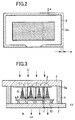
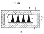
- a micro-lens type liquid crystal panel 1X having a TFT substrate 2 and a micro-lens 3 equipped facing substrate 4 glass-fiber mixed seal material 5 is coated on peripheral portion of either one of the TFT substrate 2 or the facing substrate 4 equipped with the micro-lens 3, and after that, both the TFT substrate 2 and the facing substrate 4 are superposed as to have an even gap space there-between in a conventional manufacturing method.
- the conventional micro-lens type liquid crystal panel 1X thus manufactured may have an irregularity of the gap space of about 10 -7 m order depending on a point of measurement of the liquid crystal panel 1X.
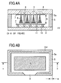
- a reference numeral 7 is an orientation film made of polyimide
- a reference numeral 8 is a liquid crystal numerator made of TN (Twisted Nematic) liquid crystal material
- a reference numeral 9 is an injection gate for the liquid crystal material in FIGs. 4A and 4B.
- the on-chip spacers 6 are formed at a shading area 11 made of a metal film within an effective picture element area 10 of the TFT substrate 2, so that a gap space G between the TFT substrate 2 and the facing substrate 4 of the effective picture element area 10 does not depend on stress to these substrates and is maintained to be constant.
- either the TFT substrate 2 or the facing substrate 4 of the micro-lens type liquid crystal panel 1Y receives the stress, and accordingly there causes the irregularity of the gap space G.
- the seal material 5 of low viscosity In order to prevent these displacement of the two facing substrates 2 and 4 of the micro-lens type liquid crystal panel 1Y, it is preferable to use the seal material 5 of low viscosity. However, if the seal material 5 of low viscosity is employed, there causes a problem such as so-called domain (residual image of a moving body) occurs or a leakage of the seal material 5 into the effective picture element area 10 occurs.
- the other method for preventing the displacement of the two substrates 2 and 4 is to reduce the amount of the seal material 5 to be coated in order to get enough margin for the displacement and to seal the two substrates 2 and 4 at peripheral portion by narrowing a width W of the seal part 5a.
- the area where the TFT substrate 2 or the facing substrate 4 receives the stress becomes large at the outside of the effective picture element area 10. This causes deterioration of an irregularity of the gap space between the two substrates 2 and 4.
- a width of a seal part is narrowed by reducing a coating quantity of seal material in order to get an enough margin for a displacement of the two substrates upon superposing and the two substrates effectively sealed with a dot-type or a linear-type seal at an outside of an effective picture element area of the liquid crystal display panel in order to prevent the stress to such area of the two substrates.
- the present invention presents a liquid crystal display apparatus, in which two facing substrates of a liquid crystal panel are sealed at a seal part provided on peripheral portion of the facing substrates and these two facing substrates are sealed by a dot-shaped or a linear-shaped seal part at an outside of an effective picture element area.
- this invention is able to apply to a micro-lens type liquid crystal panel having on-chip spacers between a TFT (Thin Film Transistor) substrate and a micro-lens equipped facing substrate.
- Such micro-lens type liquid crystal panel of the present invention has dot-shaped or the linear-shaped seal parts as the outside seal part of the effective picture element area at an injection gate for liquid crystal material and at neighbor of corner parts of the effective image element area, and further the liquid crystal panel of this invention has the linear-shaped seal part along peripheral portion of the effective picture element area which is positioned opposite to the injection gate for liquid crystal material.
- two facing substrates of a liquid crystal panel are sealed together at peripheral portion of the two facing substrates using seal material and further such seal material is coated in dot-shaped or linear-shaped form on outside and peripheral portion of the effective picture element area in addition.
- a TFT substrate and a micro-lens equipped facing substrate are superposed and sealed together with seal material after providing on-chip spacers between these two substrates.
- the seal material is coated in dot-shaped form at an injection gate for liquid crystal material and on neighbor of corner portions of the effective picture element area of the substrate and also coated in linear-shaped form at peripheral portion of the effective picture element area which is opposite to the injection gate for liquid crystal material.
- FIGs. 1A and 1B are a side sectional view and a plan view of a liquid crystal panel in a liquid crystal display apparatus of this invention, wherein the liquid crystal display apparatus includes a micro-lens type liquid crystal panel 1 comprised of on-chip spacers 6 between a TFT substrate 2 and a micro-lens equipped facing substrate 4.
- the TFT substrate 2 may include TFT (Thin Film Transistor) devices having active layers made of either poly-crystal silicon or amorphous silicon.
- the TFT substrate 2 and the facing substrate 4 are superposed together at a seal part 5a at a peripheral portion of the two facing substrates 2 and 4, and further even at an outside of an effective image element area 10 (the area between the effective image element area 10 and the seal part 5a), the TFT substrate 2 and the facing substrate 4 are superposed and sealed together at a plurality of dot-shaped seal parts 5b or a linear-shaped seal part 5c.
- the micro-lens equipped facing substrate 4 means a substrate on which transparent resin having different refraction factors integrally formed on a facing plate to form a plurality of micro-lens in order to effectively use the incident light.
- the micro-lens type liquid crystal panel 1 is fabricated by superposing and sealing the TFT substrate 2 and the micro-lens 3 equipped substrate 4 using the seal material 5.
- the on-chip spacers 6, which are made of acryl resin and fabricated using a TFT fabrication processing, are formed in advance either one of the TFT substrate 2 or the micro-lens 3 equipped facing substrate 4 within the effective picture element area 10.
- the seal material 5 is coated not only on peripheral portion of the substrates but also on outside of the effective picture element area 10 in dot-shaped form or linear-shaped form, then the seal material 5 is stiffened.
- a width W of the seal part 5a on the peripheral portion of the substrate is narrowed to 0.7 to 1.2 mm at the seal part 5a by reducing the coating amount of the seal material 5 in order to obtain enough margin for the displacement of the two substrates 2 and 4.
- the dot-shaped seal part 5b or the linear-shaped seal part 5c in the outside of the effective picture element area are provided for reducing the gap space between the substrates 2 and 4, more concretely one of the dot-shaped seal part 5a is provided at a space where the on-chip spacer 6 is not positioned in the injection gate for liquid crystal material 9, three of the dot-shaped seal part 5a are provided at a neighbor of two corners of the injection gate for liquid crystal material 9 side of the effective picture element area 10, one of the dot-shaped seal part Sb is respectively provided at neighbor of two corners opposite to the injection gate for liquid crystal material 9 side of the effective picture element area 10, one of the dot-shaped seal part 5b is respectively provided there-between and a linear-shaped seal part 5c is provided at a space opposite to the injection gate for liquid crystal material 9 and along an edge of the effective picture element area 10.
- a diameter of each dot-shaped seal part 5b is preferably 0.5 to 1.2 mm and a width of the linear-shaped seal part 5c is preferably 0.5 to 1.2 mm and a length thereof is 15 to 35 mm in a standpoint of reducing coating amount of the seal material 5, but those dimensions depend on the size of the liquid crystal panel as to cover 90% of peripheral portion of the liquid crystal panel.
- filling materials to be such as glass fiber or plastic micro-particle are preferably mixed into epoxy-based or acryl-based thermosetting adhesive or ultraviolet curing adhesive as the seal material used to form the seal part 5a, the dot-shaped seal parts 5b and the linear-shaped seal part 5c of the two substrates.
- Such filling materials become support posts for the gap space G.
- coating process for such seal material is done by painting , dispersal systems and so on.
- a liquid crystal panel is not limited to one illustrated in FIGs. 1A and 1B.
- size, the number and position of the dot-shaped seal parts 5b and the linear-shaped seal part 5c provided at the outside of the effective picture element area depend on a design of a TFT substrate or characteristics of a liquid crystal panel itself and may be changed or adjusted.
- liquid crystal panel 1 having the on-chip spacers 6 are explained in FIGs. 1A and 1B, but this invention can be applied to a liquid crystal panel having spherical spacers between TFT and CF facing substrates. Namely, seal material is coated not only on the peripheral part of one the two substrates but also coated on spaces between the effective picture element area in dot-shaped or linear-shaped form. After that these two substrates are superposed together. In this case, the resultant liquid crystal panel is to have dot-shaped or linear-shaped seal part at the outside of the effective picture element area besides on the peripheral portion of the substrate.
Landscapes
- Physics & Mathematics (AREA)
- Nonlinear Science (AREA)
- Mathematical Physics (AREA)
- Chemical & Material Sciences (AREA)
- Crystallography & Structural Chemistry (AREA)
- General Physics & Mathematics (AREA)
- Optics & Photonics (AREA)
- Liquid Crystal (AREA)
Applications Claiming Priority (2)
| Application Number | Priority Date | Filing Date | Title |
|---|---|---|---|
| JP2000095947A JP2001281677A (ja) | 2000-03-30 | 2000-03-30 | 液晶表示装置 |
| JP2000095947 | 2000-03-30 |
Publications (2)
| Publication Number | Publication Date |
|---|---|
| EP1139155A2 true EP1139155A2 (fr) | 2001-10-04 |
| EP1139155A3 EP1139155A3 (fr) | 2002-08-07 |
Family
ID=18610775
Family Applications (1)
| Application Number | Title | Priority Date | Filing Date |
|---|---|---|---|
| EP01106688A Withdrawn EP1139155A3 (fr) | 2000-03-30 | 2001-03-16 | Appareil d'affichage à cristal liquide et son procédé de fabrication |
Country Status (4)
| Country | Link |
|---|---|
| US (1) | US20010026346A1 (fr) |
| EP (1) | EP1139155A3 (fr) |
| JP (1) | JP2001281677A (fr) |
| KR (1) | KR20010095077A (fr) |
Families Citing this family (6)
| Publication number | Priority date | Publication date | Assignee | Title |
|---|---|---|---|---|
| KR100862074B1 (ko) * | 2002-12-12 | 2008-10-09 | 엘지디스플레이 주식회사 | 역사다리꼴 액정주입구가 형성된 씰 패턴을 포함하는액정표시장치용 액정패널 |
| JP4207599B2 (ja) * | 2003-02-24 | 2009-01-14 | ソニー株式会社 | 液晶パネルの製造方法 |
| JP4372648B2 (ja) | 2004-09-13 | 2009-11-25 | シャープ株式会社 | 液晶表示装置およびその製造方法 |
| KR20070071492A (ko) * | 2005-12-30 | 2007-07-04 | 엘지.필립스 엘시디 주식회사 | 액정표시소자 및 그 제조방법 |
| KR20130063372A (ko) * | 2011-12-06 | 2013-06-14 | 삼성디스플레이 주식회사 | 3차원 영상 표시 장치 |
| US20190129210A1 (en) * | 2017-10-31 | 2019-05-02 | Wuhan China Star Optoelectronics Technology Co., Ltd | Liquid crystal panel and manufacture method thereof, liquid crystal display device |
Family Cites Families (7)
| Publication number | Priority date | Publication date | Assignee | Title |
|---|---|---|---|---|
| JPS5724917A (en) * | 1980-07-23 | 1982-02-09 | Hitachi Ltd | Multilayer liquid crystal panel |
| JPH05289090A (ja) * | 1992-02-21 | 1993-11-05 | Samsung Electron Co Ltd | 液晶表示装置のシールパターン |
| JPH06265863A (ja) * | 1992-11-09 | 1994-09-22 | Sony Corp | プラズマアドレス液晶表示装置 |
| JPH1096897A (ja) * | 1996-07-31 | 1998-04-14 | Canon Inc | 液晶素子、その製造方法及び該液晶素子を備えた液晶表示装置 |
| JPH10153785A (ja) * | 1996-09-26 | 1998-06-09 | Toshiba Corp | 液晶表示装置 |
| JP3249077B2 (ja) * | 1996-10-18 | 2002-01-21 | キヤノン株式会社 | マトリクス基板と液晶装置 |
| DE69834021T2 (de) * | 1997-02-13 | 2006-11-16 | Koninklijke Philips Electronics N.V. | Optisches schaltelement und kamera mit solchem element |
-
2000
- 2000-03-30 JP JP2000095947A patent/JP2001281677A/ja active Pending
-
2001
- 2001-03-16 EP EP01106688A patent/EP1139155A3/fr not_active Withdrawn
- 2001-03-29 KR KR1020010016424A patent/KR20010095077A/ko not_active Withdrawn
- 2001-03-30 US US09/822,575 patent/US20010026346A1/en not_active Abandoned
Also Published As
| Publication number | Publication date |
|---|---|
| US20010026346A1 (en) | 2001-10-04 |
| JP2001281677A (ja) | 2001-10-10 |
| KR20010095077A (ko) | 2001-11-03 |
| EP1139155A3 (fr) | 2002-08-07 |
Similar Documents
| Publication | Publication Date | Title |
|---|---|---|
| US8264657B2 (en) | Liquid crystal display panel and method of manufacturing the same | |
| KR100796109B1 (ko) | 스페이서가 구비된 기판, 액정 표시 패널, 패널의 제조 방법 및 액정 표시 패널의 제조 방법 | |
| KR100685949B1 (ko) | 액정표시소자 및 그 제조방법 | |
| EP0772071B1 (fr) | Elément d'affichage à cristal liquide et son procédé de fabrication | |
| RU2472187C2 (ru) | Подложка цветного фильтра и жидкокристаллическое устройство отображения | |
| US10551671B2 (en) | Display panel with light converting layer therein, display device including the same and method of manufacturing the same | |
| JPS63128315A (ja) | 液晶表示素子 | |
| US20150146130A1 (en) | Liquid Crystal Display Panel and Manufacturing Method for the Same | |
| US20080062374A1 (en) | Liquid crystal display device and production method thereof | |
| US20110058130A1 (en) | Liquid crystal display device and its manufacturing method | |
| US20210181558A1 (en) | Display panel and display device | |
| CN112083605B (zh) | 液晶面板、显示装置及液晶面板的配向方法 | |
| CN106033163A (zh) | 显示面板 | |
| US8629969B2 (en) | Liquid crystal display panel and method of manufacturing the liquid crystal display panel | |
| EP1139155A2 (fr) | Appareil d'affichage à cristal liquide et son procédé de fabrication | |
| US20050140915A1 (en) | Liquid crystal display device having column spacers and method of fabricating the same | |
| KR101983214B1 (ko) | 씨오티 구조 액정표시장치 | |
| JPH11183915A (ja) | アクティブマトリクス型液晶表示装置 | |
| JP6041468B2 (ja) | 液晶表示パネル | |
| US10802314B2 (en) | Liquid crystal display device | |
| US7297223B2 (en) | Process and structure of liquid crystal panel with one drop fill | |
| US20030122763A1 (en) | Liquid crystal display device and method of fabricating the same | |
| CN1885138B (zh) | 液晶显示器件的制造方法 | |
| JP2010054552A (ja) | 液晶表示装置 | |
| CN106154619A (zh) | 显示面板 |
Legal Events
| Date | Code | Title | Description |
|---|---|---|---|
| PUAI | Public reference made under article 153(3) epc to a published international application that has entered the european phase |
Free format text: ORIGINAL CODE: 0009012 |
|
| AK | Designated contracting states |
Kind code of ref document: A2 Designated state(s): AT BE CH CY DE DK ES FI FR GB GR IE IT LI LU MC NL PT SE TR |
|
| AX | Request for extension of the european patent |
Free format text: AL;LT;LV;MK;RO;SI |
|
| PUAL | Search report despatched |
Free format text: ORIGINAL CODE: 0009013 |
|
| AK | Designated contracting states |
Kind code of ref document: A3 Designated state(s): AT BE CH CY DE DK ES FI FR GB GR IE IT LI LU MC NL PT SE TR |
|
| AX | Request for extension of the european patent |
Free format text: AL;LT;LV;MK;RO;SI |
|
| 17P | Request for examination filed |
Effective date: 20030107 |
|
| AKX | Designation fees paid |
Designated state(s): DE GB NL |
|
| 17Q | First examination report despatched |
Effective date: 20030320 |
|
| STAA | Information on the status of an ep patent application or granted ep patent |
Free format text: STATUS: THE APPLICATION IS DEEMED TO BE WITHDRAWN |
|
| 18D | Application deemed to be withdrawn |
Effective date: 20040729 |