EP1156431A2 - System zur Herstellung einer Halbleiter integrierter Schaltung - Google Patents
System zur Herstellung einer Halbleiter integrierter Schaltung Download PDFInfo
- Publication number
- EP1156431A2 EP1156431A2 EP01250174A EP01250174A EP1156431A2 EP 1156431 A2 EP1156431 A2 EP 1156431A2 EP 01250174 A EP01250174 A EP 01250174A EP 01250174 A EP01250174 A EP 01250174A EP 1156431 A2 EP1156431 A2 EP 1156431A2
- Authority
- EP
- European Patent Office
- Prior art keywords
- data
- center
- client
- manufacturing
- integrated circuit
- Prior art date
- Legal status (The legal status is an assumption and is not a legal conclusion. Google has not performed a legal analysis and makes no representation as to the accuracy of the status listed.)
- Ceased
Links
Images


Classifications
-
- H—ELECTRICITY
- H10—SEMICONDUCTOR DEVICES; ELECTRIC SOLID-STATE DEVICES NOT OTHERWISE PROVIDED FOR
- H10P—GENERIC PROCESSES OR APPARATUS FOR THE MANUFACTURE OR TREATMENT OF DEVICES COVERED BY CLASS H10
- H10P95/00—Generic processes or apparatus for manufacture or treatments not covered by the other groups of this subclass
-
- G—PHYSICS
- G06—COMPUTING OR CALCULATING; COUNTING
- G06F—ELECTRIC DIGITAL DATA PROCESSING
- G06F16/00—Information retrieval; Database structures therefor; File system structures therefor
Definitions
- the present invention relates to a system of manufacturing a semiconductor integrated circuit. Particularly, the invention relates to a fabrication system for an application-specific integrated circuit (ASIC).
- ASIC application-specific integrated circuit
- JP-A Japanese Unexamined Patent Publication
- a recent tendency is mainly directed to standardized integrated circuits (ICs) prevail, but ASICs are also supported by particular demands.
- the demands relate to the realization of system large-scale integrated circuits (LSIs) according to needs of users who attempt discrimination of products from those developed by their competitors and practical use of large-diameter wafers.
- LSIs system large-scale integrated circuits
- ASICs directly affects clients' products, they should be developed, designed, and fabricated in a close relationship between a client and a semiconductor manufacturer with an organizational system that allow cooperative joint-work organization. This system requires agreements to be made between the client and the semiconductor manufacturer for various matters, for example, work interfaces, design specifications, developing tools, product quality, test data, production periods, and costs.
- a client releases layout data from an FPGA developing tool (FPGA: field programmable gate array) via the Internet (see http://www,quicklogic.com/webasic ).
- FPGA field programmable gate array
- a manufacturing center writes the received data into FPGA chips, and sends completed circuit chips to the client via a normal transporting means.
- a client creates layout data for FPGAs of a different company (Altera Corp.), and sends the data via the Internet (see http://www.clear-logic.com/pressrelease/11-29/99.htm ).
- a manufacturing center uses the received data, thereby manufactures products of its own, and sends completed products (circuit chips) to the client by means of a normal transporting means.
- An object of the present invention is to provide an improved system of manufacturing a semiconductor integrated circuit, which allows a client to perform suitable and flexible ordering that meets product market conditions.
- Another object of the invention is to provide an improved system of manufacturing a semiconductor integrated circuit, where a client can obtain benefits of reduction in a product development period, reduction in costs and improvement in quality of the product.
- Still another object of the invention is to provide an improved system of manufacturing a semiconductor integrated circuit, where a semiconductor manufacturer can make stable production plans.
- Yet another object of the invention is to provide an improved system of manufacturing a semiconductor integrated circuit, which can be flexibly built by a semiconductor manufacturer to meet market conditions.
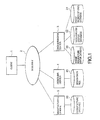
- a data-managing center (3), a designing center (4), and a manufacturing center (5) which are operation centers on the side of a semiconductor manufacturer, and a client (1) are connected together via the Internet (2).
- Each of the operation centers (3, 4, and 5) uses information contained in databases (31, 32, and 33) provided in the data-managing center (3), performs two-way communication with the client (1), and thereby progresses the production of semiconductor integrated circuit.
- the system of manufacturing a semiconductor integrated circuit may be configured such that operation centers (3, 4, and 5), which are the data-managing center (3), the designing center (4), and the manufacturing center (5), are connected together via the Internet (2).
- the data-managing center (3) comprises databases including a cost/number-of-days database (31) containing data representing courses for manufacturing the semiconductor integrated circuit, each of which has attributes of costs and the number of days in units of a product type and an urgency degree of the semiconductor integrated circuit; a reservation status database (32) containing data of an acceptable reservation quantity in units of the product type and the urgency degree of the semiconductor integrated circuit and in units of chip-completion date; and a design/manufacture status database (33) containing data representing statuses of ordering, releasing, designing, and manufacturing in units of a client.
- a cost/number-of-days database (31) containing data representing courses for manufacturing the semiconductor integrated circuit, each of which has attributes of costs and the number of days in units of a product type and an urgency degree of the semiconductor integrated circuit
- the data-managing center (3) communicates with the client (2) to thereby perform data management.
- the designing center (4) communicates with the client (1), performs designing of the semiconductor integrated circuit according to release data from the client, and outputs layout data as a product of the designing.
- the manufacturing center (5) performs manufacturing of the semiconductor integrated circuit acccrding to manufacture data that is released from one of the designing center and the client and that is intended for use in the manufacturing.
- Each of the operation centers (3, 4, and 5) uses information contained in the databases (31, 32, and 33) provided in the data-managing center (3), performs two-way communication with the client (1), and thereby progresses the production of the semiconductor integrated circuit.
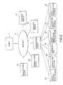
- system of manufacturing a semiconductor integrated circuit may be configured such that operation centers (41, 42, 51, and 52), which are the data-managing center (3); a plurality of designing centers (41 and 42), and a plurality of manufacturing centers (51 and 52), are connected together via the Internet.
- the data-managing center (3) comprises databases (31, 32, and 33) including the cost/number-of-days database (31) containing data representing courses for manufacturing the semiconductor integrated circuit, each of which has attributes of costs and the number of days in units of a product type and an urgency degree of the semiconductor integrated circuit; the reservation status database (32) containing data of an acceptable reservation quantity in units of the product type and the urgency degree of the semiconductor integrated circuit and in units of chip-completion date; the design/manufacture status database (33) containing data representing statuses of ordering, releasing, designing, and manufacturing in units of a client.
- the data-managing center (3) communicates with the client (1) to thereby perform data management.
- Each of the designing centers (41 and 42) closely communicates with the client (1), performs designing of the semiconductor integrated circuit according to release data provided from the client (1), and outputs layout data as a product of the designing.
- Each of the manufacturing centers (51 and 52) performs manufacturing of the semiconductor integrated circuit according to manufacture data that is released from one of the designing center (41 or 42) and the client (1) and that is intended for use in the manufacturing.
- the data-managing center (1), and each of the designing centers (41 and 42) and the manufacturing centers (51 and 52) uses information contained in the databases (31, 32, and 33) provided in the data-managing center (3), performs two-way communication with the client (1), and thereby progresses the production of the semiconductor integrated circuit.
- the data-managing center (3) may comprise a design data file (40) for retaining release data released from the client (1), a manufacture data file (50) for retaining the manufacture data released from one of the designing center (41 or 42) and the client (1), and a center-operation-status database (60) containing operation statuses of the operation centers (41, 42, 51, and 52).
- the data-managing center (3) is connected to the various databases (31, 32, 33, and 60) to thereby allow bilateral-communication characteristics of the Internet (2) to be used between the client (1) and each of the semiconductor-manufacturer-side operation centers (3, 4, and 5; or 41, 42, 51, and 52). Therefore, the databases (31, 32, 33, and 60) can be efficiently used.
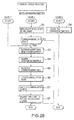
- Fig. 1 is a configuration view of an ASIC-manufacturing system according to a first embodiment of the present invention.
- a client 1 user
- ASIC manufacturer semiconductor manufacturer
- the semiconductor manufacturer includes three operation centers: a designing center 4 (designing division); a manufacturing center 5 (manufacturing division); and a data-managing center 3 that manages the exchanged data, the number of days, and costs.
- the designing center 4 has a design data file 40 containing release data released from the client 1.
- the manufacturing center 5 has a manufacture data file 50 that stores manufacture data received from the designing center 4 and/or the client 1.
- the data-managing center 3 has a cost/number-of-days database 31, a reservation status database 32, and a design/manufacture status database 33.
- each of the operation centers 3 to 5 is practically constituted of people, an information processing system, and operators of the system, it is shown as a server in Fig. 1.
- Fig. 2 shows a second embodiment of the present invention.
- the second embodiment corresponds to a case where two designing centers 41 and 42 and two manufacturing centers 51 and 52 are provided.
- the designing centers 41 and 42 may be provided in, for example, the USA; and the manufacturing centers 51 and 52 may be provided in, for example, Taiwan. Even in overseas countries, real-time communication can be performed through the Internet 2.
- the data-managing center 3 one-dimensionally controls the design data file 40 that is provided in each of the designing centers 41 and 42, and the manufacture data file 50 that is provided in each of the manufacturing centers 51 and 52. This control facilitates data communication with the client 1.
- the data-managing center 3 Upon receipt of an order from the client 1 for manufacturing of ASICs, the data-managing center 3 checks the operation status of each of the designing centers 41 and 42 and the manufacturing centers 51 and 52, and thereby selects appropriate one of the designing centers 41 and 42 and one of the manufacturing centers 51 and 52, Information required for the selection is stored in a center-operation-status database 60.
- the number of the designing centers and the manufacturing centers may be increased depending on the reservation status and the design/manufacture status.
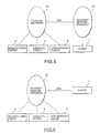
- Fig. 3 shows a third embodiment of the present invention.
- This embodiment relates to a fail-safe configuration.
- the connections of the data-managing center 3, the designing center 4, and manufacturing center 5 to the Internet 2 are mirrored, respectively.
- network-mirroring is implemented between the data-managing center 3 and each of databases 31, 32, and 33, between the designing center 4 and the design data file 40, and between the manufacturing center 5 and the manufacture data file 50.
- Fig. 4 shows a fourth embodiment.
- the fourth embodiment has a mirror server 6 relative to the data-managing center 3.
- the mirror server 6 is connected to a cost/mimber-of-days database 61, a reservation status database 62, and a design/manufacture status database 63.
- the fourth embodiment similarly to the third embodiment, has a fail-safe configuration.
- the mirror server 6 performs the same operation as the data-managing center 3. Thereby, even when a failure occurs in the data-managing center 3 during processing, the processing can be continued without problems.
- each of Figs. 3 and 4 shows the example configuration relative to the first embodiment including a manufacturing center and a designing center.
- fail-safe mechanisms similar to those described above may be provided in the second embodiment that includes the plurality of designing centers and manufacturing centers.
- Figs. 1 to 4 show conceptual configurations. In practice, however, as shown in Figs. 5 to 7, a virtual private network (VPN) is used to protect private information of the client 1 from leakage when a client receives ASIC-manufacture-related services provided by a semiconductor manufacturer,
- the "virtual private network (VPN)" is a generic name of services that allow a public network to be used as a dedicated network, and it is therefore called a "virtual closed-area network”.
- an internet service provider 21 ISP
- an in-house network 22 are involved between the client 1 and individual centers 3 to 5; and a VPN connects the internet service provider 21 and the in-house network 22.
- the individual centers 3 to 5 are connected via the in-house network 22.
- the client 1 and the internet service provider 21 are connected together via a VPN.
- Individual operation centers 3 to 5 are connected to the internet service provider 21.
- the configuration shown in Fig. 5 is advantageous in the security of private information, while the configuration shown in Fig. 6 is advantageous in the usability of the client 1.
- a VPN connects a provider standard service 211 and a semiconductor design service 212 in the internet service provider 21.
- the operation centers 3 to 5 are individually connected to the provider standard service 211 via the semiconductor design service 212.
- Fig. 8 shows operations that are performed by the client 1 to establish connection with a Web server in order to receive an ASIC-manufacturing service.
- the client 1 attempts to obtain an ISP connection authentication (ISP: Internet service provider).
- ISP Internet service provider
- the client 1 attempts to obtain a semiconductor-design-service connection authentication.
- the client 1 is qualified to receive a service that allows the client to encrypt data, such as release data, and to receive and transmit the encrypted data.
- the semiconductor-design-service connection authentication is performed using information, such as identification (ID) information allocated to the client 1, machine-specific information (such as MAC information of a network card) of the client 1, and developing-tool license information provided to the client 1.
- ID identification
- machine-specific information such as MAC information of a network card
- the client 1 To access one of the databases 31 to 33 by using ID information, the client 1 issues preallocated ID information.
- the database to be accessed accesses the client 1, obtains the ID information, and then performs authentication.
- per-client access status information can be collected.
- the collected information is analyzed to perform risk management for redesign (rework) ratios and the like in units of the client. Thereby, service fees and information disclosure limitations can be set depending on the rework ratios.
- the client 1 can use three order modes to order ASICs from a semiconductor manufacturer, These modes are a mode for designing and manufacturing, a mode only for designing, and a mode only for manufacturing.
- the mode for the designing may be classified to be more specific depending on types of release data that includes logic-design specifications, logic-design data, circuit design data, layout design data, and mask design data.
- Fig. 9 shows the relationship among the client 1, the data-managing center 3, the designing center 4, and the manufacturing center 5 when the order mode for designing and manufacturing is executed.
- the client 1 To place an order with a semiconductor manufacturer for manufacturing of ASICs, the client 1 first accesses the data-managing center 3 via the Internet 2 and makes inquiry to obtain information about whether manufacturing lines in the semiconductor manufacturer are available to handle the new order or are not available to handle the new order because of overlapped orders, and what order modes are set.
- the data-managing center 3 accesses the reservation status database 32 and the cost/number-of-days database 31, obtains necessary information, and sends a response based on the information to the client 1 via the Internet 2.
- the client 1 Upon receipt of the response, the client 1 checks the manufacturing-line status, costs, the number of days, and the like. Then, the client 1 selects from specified reservation courses an appropriate course closed to a desired course, and issues a reservation application for the selected course via the Internet 2. In response to the reservation application, the data-managing center 3 issues a reservation-reception notification to the client 1 via the Internet 2. This completes the reservation processing.
- the client 1 issues an order to the data-managing center 3 via the Internet 2, and sends release data to the data-managing center 3.
- the data-managing center 3 sends the release data to the designing center 4 via the Internet 2.
- the designing center 4 stores the release data in the design data file 40. Thereby, designing of the ASICs is started.
- the contents of designing to be carried out by the designing center 4 are different depending on the contents of a contract concluded between the client 1 and the semiconductor manufacturer. For example, a client orders overall designing, while a different client orders for designing of circuits and subsequent portions.
- the designing center 4 periodically reports the design status to the data-managing center 3. The reporting may be made to cover either the overall design or per-stage design.
- the designing center 4 sends layout data to the data-managing center 3 via the Internet 2.
- the data-managing center 3 sends the layout data to the client 1 via the Internet 2.
- layout data is not limited to back annotation data, and it refers to data that is produced on the basis of release data received on a designing center 4 from the client 1 and that is sent as a design result to the client 1.
- the client 1 checks the layout data by conducting, for example, a physical delay analysis, and reports the result to the designing center 4 via the Internet 2.
- the designing center 4 sends manufacture data to the data-managing center 3, and the data-managing center 3 releases the manufacture data to the manufacturing center 5.
- manufacture data is not limited to mask data, and it refers to data used in the manufacture in the manufacturing center 5.
- the manufacturing center 5 stores the manufacture data in the manufacture data file 50, and then starts the manufacturing of the ASICs.
- the manufacturing center 5 periodically reports the manufacturing status to the data-managing center 3.
- the manufacturing center 5 transports the completed LSI chips to the client 1 by means of normal transporting means.
- progress-status information on design, manufacture, and the like are periodically collected in the data-managing center 3. Therefore, the client 1 can obtain desired status information by accessing the data-managing center 3 through the Internet 2. Therefore, according to the present embodiment, the client 1 and the semiconductor manufacturer can progress the ASICs production by exchanging information.
- the client 1 wants to check the status of the layout data, that is, an interim report from design tools, prior to the completion of design, and modifies design on the side of the client 1. Specifically, when the client 1 detects a defect in its design, it reviews reserved schedules, costs, and the like; and when it finds the defect to be its own responsibility, it reorders for the ASICs.
- an embodiment can be conceived in which the client 1 can directly access the designing center 4 via the Internet 2. According to the embodiment configured in this way, the client 1 can directly send release data to the designing center 4 without the data-managing center 3 being involved, while the designing center 4 can directly send layout data to the client 1 but not through the data-managing center 3.
- the data-managing center 3 selects desired centers, and sends release data and manufacture data to selected centers. Specifically, after completion of designing, the selected designing center sends manufacture data to the data-managing center 3, and the data-managing center 3 sends the manufacture data to the selected manufacturing center.
- the data-managing center 3 makes referential access to the center-operation-status database 60.
- a manufacturing center to which the manufacture data is sent from the data-managing center 3 may be predetermined. In this case, the designing center 4 can directly send design data to the predetermined manufacturing center without the data-managing center 3 being involved.
- the client 1 can use three order modes to place orders with a semiconductor manufacturer for ASICs. That is, the client 1 can use the mode for designing and manufacturing, the mode only for designing, and the mode only for manufacturing.
- the example cases where designing and manufacture are ordered are illustrated in Fig. 9.
- Fig. 10 shows an example case when only manufacture is ordered.
- the client 1 sends manufacture data to the data-managing center 3.
- the data-managing center 3 sends the manufacture data, which has been received from the client 1, to the manufacturing center 5.
- the manufacturing center 5 manufactures LSI chips, and transports completed LSI chips to the client 1.
- Fig. 11 shows an example case where the client 1 places orders with a semiconductor manufacturer for designing, only.
- the data-managing center 3 sends release data received from the client 1 to the designing center 4.
- the designing center 4 sends delivery data to the data-managing center 3.
- the data-managing center 3 sends the delivery data to the client 1.
- the manufacturing center 5 does not participate the data communication in the illustrated example.
- a mode can be employed in which the client 1 and a semiconductor manufacturer closely cooperate with each other. That is, a mode for joint designing can be employed.
- Fig. 12 shows an example case where the joint designing is implemented in accordance with the second embodiment shown in Fig. 2.
- the client 1 releases release data to the data-managing center 3, then the data-managing center 3 sends the data to the designing center 41.
- the designing center 41 carries out designing according to the release data, and sends an interim design report A to the client 1 via the data-managing center 3.
- the client 1 carries out design modification in consideration of the interim design report A, and generates an interim design report B. Then, the client 1 sends the interim design report B to the data-managing center 3.
- the data-managing center 3 sends the interim design report B to the designing center 42.
- the designing center 42 carries out designing according to the interim design report B, and sends an interim design report C to the client 1 via the data-managing center 3. These steps are repeated to thereby complete final delivery data.
- a semiconductor manufacturer provides developing tools and developing libraries to the client 1 to progress development by using common tools.
- a workstation is necessary.
- ones of clients 1 posses personal computers but do not possess a workstation.
- other ones of the clients 1 do not like to procure expensive commercially available tools.
- the configuration may be built such that a CAD center is provided as a part of the data-managing center 3 to thereby provide use environments for the developing tools and commercially available tools to the clients 1.
- the client 1 can use the CAD center through the Internet 2.
- Fig. 13 shows a practical example of storage contents of the cost/number-of-days database 31.
- ASIC-manufacture courses are set in correspondence with product types of ASI Cs and urgency degrees.
- Each of the illustrated courses has costs number of days as its attributes. Referring to Fig. 13, it is understood that, as the urgency is increased as in the order from "Lowest (Special Discount)", “Second lowest (Discount)", “Regular”, “Second-highest”, “Highest”, costs are increased in proportion thereto, but the number of days is reduced in inverse-proportion thereto.
- other cases are also provided. For example, the "Second Lowest (Discount)" course is not set for a product type A, and the "Highest” course and the “Lowest (Special Discount)” course are not set for a product type D.
- Fig. 14 shows a practical example of storage contents of the reservation status database 32.
- an allowable reservation quantity is indicated at each of fields designated with the ASIC product types/courses and LSI-chip completion dates.
- Numeral "0" represents that no reservation request can be accepted
- numeral "1" represents that only one reservation request can be accepted.
- Defaults (initial values) of the acceptable reservation quantities are determined in consideration of the production capacity of a semiconductor manufacturer, market conditions, and the like. Also, the acceptable reservation quantities are reviewed according to the design/manufacture status and market conditions of a semiconductor manufacturer. In addition, upon receipt of reservation from a client 1, the acceptable reservation quantity is thereby reduced; whereas, upon receipt of cancellation for reservation, it is thereby increased.
- Fig. 15 shows a practical example of storage contents of the design/manufacture status database 33.
- each row of clients 1, an order status, a release status, a design status, and a manufacture status are shown.
- the column of the order status shows the contents of orders, and contains items of chip-specific titles "Product Name”, “Product Type”, “Course” ("Regular”, “Second-highest”, or the like shown in Figs. 13 and 14), and "Reservation Date”.
- the column of the release status contains the items of "Information Type", "Scheduled Date” of the release, and "Completion Date” of the release.
- the item “Information Type” contains the type of release information sent from the client 1, such as a logic design specification, logic design data, circuit design data, layout data, or mask data.
- the column of the manufacture status contains the items of "Responsible Manufacturing Center Name", per-step “Scheduled Date”, and per-step “Completion Date”.
- the individual fields of "Scheduled Date” are determined upon acceptance of reservation.
- the row including "EFG” as "Product Name” contains information relating to an example order mode for designing, only.
- the designing center 4 has a number of designing lines
- the manufacturing center 5 also has a number of manufacturing lines. Therefore, in view of the capacity, the designing center 4 and the manufacturing center 5 individually access the data-managing center 3, and can increase or reduce their designing resources and manufacturing resources, according to the reservation status and the design/manufacture status.
- the data-managing center 3 has the center-operation-status database 60.
- Fig. 16 shows a practical example of storage contents of the center-operation-status database 60.
- the database 60 has the item of "Number of Operating Resources", “Number of Resources", and "Operation Ratio" for each of designing centers X1, X2, ...
- One advantage available in accordance with the provision of the center-operation-status database 60 is that manufacture data of a plurality of products are incorporated and are embodied on a single wafer.
- the plurality of products may be those collected from different clients 1.
- This implements improvement in integration and efficiency of manufacture by taking the operation statuses in the individual manufacturing centers into account in the background of advancing technological development for large-diameter wafers. As a result, this improvement allows the manufacturing cost to be reduced.
- the data-managing center 3 can thus make determination with regard to the above-described factors, and can direct the manufacturing centers to mount a plurality of products on individual wafers.
- a cancellation database may be connected to the data-managing center 3.
- Fig. 17 shows a practical example of storage contents of the aforementioned cancellation database.
- Fig. 13 showing the cost/number-of-days database 31
- the figure shows ASIC-manufacture-reservation cancellation charges in fields of the ASIC product types and the urgency degrees.
- the number of days represents the number of remaining days in the period up to a scheduled release date.
- the cancellation charge varies depending on the number of remaining days in the period up to the scheduled release date. Specifically, the smaller the number of remaining days, the higher the charge is set, and also, the higher the price of the product type and the urgency degree, the higher the cancellation charge is set.
- FIG. 18 shows a practical example of storage contents of the insurance database that stores data representing premiums of a redesign insurance and a cancellation insurance.
- a redesign-insurance premium and a cancellation-insurance premium are set in fields of the product types and the urgency degrees.
- the redesign-insurance premium is an insurance premium necessary either for providing redesign services free of charge or discounting a redesign fee, in consideration of predetermined times of redesign services.
- the cancellation-insurance premium is an insurance premium necessary for discounting a cancellation charge when a reservation cancellation occurs.
- a semiconductor manufacturer can request the client 1 to pay the aforementioned insurance premiums.
- a per-client design/manufacture historical-log database may be connected to the data-managing center 3.
- Fig. 19 shows a practical example of the storage contents of the per-client design/manufacture historical-log database.
- the per-client design/manufacture historical-log database contains a current design/manufacture status and a past design/manufacture status in fields of the clients 1, the product names, and the product types.
- the data base contains past design and manufacture order quantities, the numbers of past redesign (rework due to defects) occurrences, past reservation-cancellation ratios, with regard to clients 1.
- Product information data in the column "Current Product” are stored (registered) in the database upon acceptance of a reservation request, and they are deleted upon completion of scheduled designing and manufacturing.
- an asterisk (*) is entered in the sub-column “Cancellation” of the column “Current Product.”
- the product information data are deleted from the "Current Product” column.
- the “Total” column contains totals of past-to-current data corresponding to the respective fields in the "Current Product” column.
- the data stored in the above-described per-client design/manufacture historical-log database is used to adjust service fees.
- a semiconductor manufacturer offers a discount to the client 1 who issues a large number of orders for designing/manufacturing and to a good client 1 for which the redesign occurrence ratio is low.
- the semiconductor manufacturer offers a higher redesign insurance premium to the client 1 for which the redesign occurrence ratio is high.
- a semiconductor manufacturer uses the database to limit reservations, to disable long-term reservations, and to limit the courses, for example, to allow only courses except for the second-highest course.
- a revision-management database may be connected to the data-managing center 3.
- the revision-management database stores design data parameters in fields of the clients 1, the product types, and the revision levels of layout data.
- the design data parameters are data extracted from layout data, and the client 1 can make examination of the layout, such as delay analyses, according to the design data parameter.
- Fig. 20 relates to a practical example of storage contents of the revision-management database, where design data parameters are shown with regard to product names AAG and AAH for a client AAA1 at fields of the revision levels.
- control is performed to automatically return to the data to that of the previous revision.
- the performance can be estimated by using relevant design data parameters.
- Fig. 21 shows a status where execution logs (reports) are input to the revision-management database.
- the designing center 4 serially registers individual execution logs of steps, which starts with checking of a release object provided from the client 1 and ends with the creation of mask data, into the revision-management database.
- the revision-management database is segmented into a revision-management portion and a know-how portion.
- the revision-management portion stores developing tools and developing libraries. They need to match with those of each semiconductor manufacturer so that a consistent developing environment is shared between the client 1 and the semiconductor manufacturer. Therefore, when the client 1 builds the developing environment on a workstation of its own and starts on designing, the client 1 sends revision information to its semiconductor manufacturers.
- the semiconductor manufacturer when the semiconductor manufacturer has received release data from the client 1, the semiconductor manufacturer sends revision information to the client 1. In addition, when the semiconductor manufacturer has performed data-update or detects an occurrence of a defect, the semiconductor manufacturer sends the latest revision information to the client 1.
- the know-how portion stores design know-how data in addition to the above-described design data parameters design data.
- the semiconductor manufacturer uses the information stored in the know-how portion to develop and provide a higher-performance design system to the client 1.
- the design know-how data includes, for example, layout data relative to design data released by the client 1, data on usage instances of developing tools, data on commercially available tools, data on problems caused by using the commercially available tools, and data on relations between circuit configurations and the number of days used for realizing the circuit configurations. Therefore, since the design know-how data can be used to reflect special factors on estimations of standard performancs and schedules, the estimations are improved in precision.
- the client may not have corresponding design data. Even in this event, the above-described design know-how allows problem-preventing redesigning to be implemented.
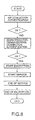
- the client 1 inquires information about schedules, costs, and capacity (step A1) from the data-managing center 3.
- the data-managing center 3 performs number-of-days/cost/reservation-status-reporting processing (shown in Fig. 24 in detail) (step A2) and sends a response to the client 1.
- the client 1 selects an optimal product type, course, and schedule, and issues a reservation request to the data-managing center 3 (step A3).
- the data-managing center 3 performs reservation-acceptance determining processing (shown in Fig. 26 in detail) (step 4), and determines whether the reservation request is acceptable (step A5), in consideration of the processing result.
- step A5 if the reservation request is determined to be unacceptable, the data-managing center 3 issues a reservation-unaccepted notification to the client 1 (step A6). Upon receipt of the notification, the client 1 reconsiders its reservation request to seek for alternative reservation conditions (step A7). As a result, if the client 1 determines the alternative conditions to be acceptable, it returns to step A1, and carries out the steps A1 to A6 again.
- step 5 if the reservation request is determined to be acceptable, the data-managing center 3 performs designing-center/manufacturing-center selecting processing (shown in Fig. 27 in detail) (step A8), and issues reservation-accepted notifications to the client 1 and selected designing center and manufacturing center (step A9).
- the client 1 prepares a release object including release data in the period by a reserved release date (step A10). In the period, however, since a case can occur in which the release cannot be prepared for some reasons, determination is made at a release-execution time (step A11) whether the release is possible. If the release is determined to be impossible, a cancellation notification (step A12) is issued to the data-managing center 3. In response, the data-managing center 3 performs canceling processing (shown in Fig. 28 in detail) (step A13).
- the client 1 sends the release object to a recipient of the release (designing center in the present example) (step B1 in Fig. 23).
- the designing center creates layout data (step B2).
- the designing center reports the design-progress status to the data-managing center 3 (step B2). Therefore, depending on the necessity, the client 1 can inquire ofthe data-managing center 3 about the design progress status (step B8).
- the data-managing center 3 reports the design-progress status to the client 1 (step B4).
- the designing center Upon completion of the design, the designing center sends a layout data to the client 1 (step B2).
- the client 1 verifies the layout data (step B5), and determines whether the layout data is acceptable (step B6). If the layout data is unacceptable, the client 1 issues a rejection notification to the designing center (step B7).
- the designing center determines whether it can perform redesigning to meet the conditions of schedules and costs initially agreed upon (step B8). If it determines the redesigning to be possible, it returns to step B2, and start the redesigning. A certain number of redesigning processes can be performed, but it depends on the factors, such as the product type and the course. At step B8, if redesigning is determined to be impossible, redesigning processing (shown in Fig.
- step B9 is performed in the data-managing center 3 (step B9).
- step B6 if the layout data is determined to be acceptable, the client 1 issues an acceptance notification to the designing center (step B10). According to the notification, the designing center creates manufacture data from the layout data (step B11), and releases the manufacture data to the manufacturing center (step B12).
- the manufacturing center manufactures LSI chips by using the manufacture data (step B 13).
- the manufacturing center reports the progress status to the data-managing center 3 (step B13).
- the client 1 can inquire of the data-managing center 3 about the progress status of the manufacture when it desires (step B3).
- the data-managing center 3 reports the progress status to the client 1 (step B4).
- the manufacturing center transports LSI chips to the client 1 (step B13).
- Figs. 24 to 30 show detailed flows of the routine processing in Figs. 22 and 23.
- Fig. 24 is a detailed flowchart of the number-of-days/cost/reservation-status reporting processing (step A2 in Fig. 22).
- the data-managing center 3 accesses the reservation status database 32, the cost/number-of-days database 31, the cancellation database, the insurance-premium database, and the per-client design/manufacture historical-log database, and reads data out of the individual databases (steps C1 to C5), Then the data-managing center 3 performs per-client customizing processing (shown in Fig. 25 in detail) (step C6), and reports post-customization costs, number of days, acceptable reservation quantity, cancellation charge, and insurance premium to the client 1 (step C7).
- Fig. 25 is a detailed flowchart of the per-client customizing processing (step C6) shown in Fig. 24.
- the data-managing center 3 sets each of the acceptable reservation quantities to zero for reservation-restriction-target product types in some or all of the courses (step D1).
- the data-managing center 3 sets the acceptable reservation quantities to zero for those for which the periods from the current time to the release time are long. Thereby, the data-managing center 3 disables a long-term reservation to be made by the client 1 (step D1).
- the data-managing center 3 reduces fees for the client 1 applicable to the conditions that the total design order quantity, the total manufacture quantity, the design order quantity for the current product type, the manufacture quantity for the current product type are large; and the total redesign ratio or the redesign ratio for the current product type are low (step D2).
- the data-managing center 3 increases the fees (step D2).
- the data-managing center 3 increases the cancellation charge and the cancellation-insurance premium (steps D3 and D4).
- the data-managing center 3 reduces the cancellation charge and the cancellation-insurance premium (steps D3 and D4). Furthermore, for applicable to the conditions that the total redesign occurrence ratio is high or that the number of redesign times for the current product type is large, the data-managing center 3 increases the redesign insurance premium (step D5). Concurrently, the data-managing center 3 reduces the redesign insurance premium for the client 1 applicable to the inverse condition of the above (step D5).
- Fig. 26 is a detailed flowchart of reservation-acceptance determining processing (step A4 in Fig. 22).
- the data-managing center 3 accesses the reservation status database 32 to judge whether desired product type, course, and schedule can be reserved (step E1). As a result, if the reservation is impossible (step E2), the data-managing center 3 terminates the reservation-acceptance determining processing. If the reservation is possible (step E2), the data-managing center 3 subtracts one from an acceptable reservation quantity for the corresponding data stored in the reservation status database 32 (step E3), in order to update the acceptable reservation quantity. Then, the data-managing center 3 writes the reservation information to the design/manufacture status database 33 (step E4), and also writes the reservation information to the per-client design/manufacture historical-log database (step E5).
- Fig. 27 is a detailed flowchart of designing-center/manufacturing-center selecting processing (step AS in Fig. 22).
- the data-managing center 3 accesses the center-operation-status database 60, and reads operation data corresponding to the reserved schedule (step F1) out of the database 60. Subsequently, the data-managing center 3 selects a designing center and a manufacturing center that can be allocated to the order, and updates reservation quantities in the corresponding reservation fields (number of operating resources to be written in the fields under "Number of Operating Resource" items shown in Fig. 16) (step F2). Subsequently, the data-managing center 3 writes the names of the reserved centers in the fields of the responsible designing center and the responsible manufacturing center in the design/manufacture status database (step F3).
- Fig. 28 is a detailed flowchart of canceling processing (step A13 in Fig. 22).
- the canceling processing has three types of processing: automatic canceling processing (Case 1); canceling processing to handle a canceling request received from the client 1 (Case 2); and canceling processing to handle a case where a cancellation charge is paid by the client 1 (Case 3).
- the data-managing center 3 accesses the design/manufacture status database 33, searches for a case where release data is not yet released from the client 1 even after a scheduled release date (step G1), and thereby determines whether data corresponding the case exists in the database (step G2).
- the data-managing center 3 adds one to the acceptable reservation quantity of the corresponding data in the reservation status database 32 (step G3) to update the quantity, and deletes corresponding data from the design/manufacture status database 33 (step G4).
- the data-managing center 3 also enters a mark in the corresponding field of the current-product-type cancellation field in the per-client design/manufacture historical-log database (step G5), and updates the corresponding cancellation ratio in the "Total" field in the database (step G6).
- the data-managing center 3 calculates the cancellation charge according to the storage contents of the cancellation database (step G7), and requests the client 1 to pay the cancellation charge (step G8).
- the data-managing center 3 carries out the routine from steps G3 to G8.
- the data-managing center 3 carries out only processing (step G9) to delete the corresponding data from the "Product Type" column of the per-client design/manufacture historical-log database.
- Fig. 29 is a detailed flowchart of redesigning processing (step B9 in Fig. 23).
- the data-managing center 3 estimates redesign conditions (necessary schedules and costs) in accordance with the initial schedule and costs and the causes for the redesign (step H1).
- the data-managing center 3 accesses the reservation status database 32 to cancel the initial reservation, and reserves a possible course that satisfies the redesign conditions (step H2).
- the data-managing center 3 accesses the center design/manufacture status database 33, cancels the initial reservation, and reserves possible operation centers that satisfy the redesign conditions (step H3).
- the data-managing center 3 submits an estimation result (the course, schedules, additional costs, etc.) to the client 1 (step H4).
- the client 1 determines whether to cancel the request for the redesign reservation (step H5).
- the client 1 issues a cancellation notification (step H6).
- the data-managing center 3 performs canceling processing (shown in Fig. 28) (step H7).
- the client 1 issues a redesign execution notification to the data-managing center 3 (step H8).
- the data-managing center 3 adds one to the number of redesign times on the corresponding field in the current product column (step H9), and updates the corresponding field of redesign occurrence ratio in the "Total" field (step H10).
- the data-managing center 3 After the client 1 inputs requirements for the costs, delivery, performance, chip sizes, and the like, the data-managing center 3 totally considers the requirements of the client 1 by accessing and referring to data contained in, for example, specifications of individual product types, the cost/number-of-days database 31, the reservation status database 32, and the design/manufacture status database 33. As a result, the data-managing center 3 can estimate most suitable product types, courses, and the like, and can submit the estimation result to the client 1. On the other hand, when the client 1 submits design data (data to be used by the semiconductor manufacturer to design the ordered ASICs), the designing center 4 in the semiconductor manufacturer can estimate the performance and the areas of the chips by using developing tools.
- the semiconductor manufacturer can make charge free or can prepare the estimation to include price-reduction when an order is issued therefor.
- the semiconductor manufacturer can temporarily estimate the performance, the areas of the chips, and the like, in accordance with past design data obtained through reference to the data in the revision-management database, and can submit the estimation to the client 1. Also in this case, the estimation is handled similarly to that described above.
- Fig. 30 is a flowchart of estimating processing to be performed in response to a request made from the client 1 to the data-managing center 3 for estimation of the ASIC performance.
- the client 1 makes an estimation-information-submittal request to the data-managing center 3 (step I1).
- the data-managing center 3 notifies a plurality of outlined estimating methods, and information and costs that are required for each of the estimating methods (step I2).
- the client 1 selects desired one of the estimating methods, and notifies the title of the selected estimating method and information necessary for the estimation to the data-managing center 3 (step I3).
- the data-managing center 3 performs per-estimating-method processing (see Fig.
- step I4 the data-managing center 3 requests the client 1 to pay a fee for the estimation (step I5).
- the client 1 receives the estimation result, and pays the fee for the estimation depending on the requirement (step I6).
- Fig. 31 is a detailed flowchart of a first estimating method in the per-estimating-method processing at step 14 in Fig. 30.
- the data-managing center 3 selects a product type that satisfies requirements of the client 1 for the performance according to specifications of various product types (which are stored in a database (not shown))(step J1). Thereby, the data-managing center 3 selects a course satisfying the requirements of the client 1 for the schedule and costs, taking into consideration data on the corresponding product type which is contained in the reservation status database 32 and the cost/number-of-days database 31 (step J2). In this case, if no product type satisfying all the requirements of the client 1 can be detected, the data-managing center 3 detects one or more alternative courses. Subsequently, the data-managing center 3 presents information on selected product types and schedules and costs therefor to the client I (step J3).
- Fig. 32 is a detailed flowchart of a second estimating method in the per-estimating-method processing at step 14 in Fig. 30.
- the data-managing center 3 extracts design parameters that are used for comparison (step K1).
- the data-managing center 3 retrieves design parameters proximate to the design parameters extracted from the data submitted by the client 1, and reads out performance data therefrom (step K2).
- the performance data means data of speeds, areas, and consumption power.
- the data-managing center 3 modifies the performance data read out depending on the necessity, and thereby determines estimated performance values (step K3). This means that, for example, although no data matching the data submitted by the client 1 exists in the revision-management database, when a plurality of items of data proximate thereto exist, the mean value of values represented by the proximate data is used as estimation values.
- the processing to be performed in the designing center 4 may be automated so that interstep losses are eliminated, and design-progress-status information is automatically submitted to the client 1. This enables the client 1 to proceed subsequent processing at its discretion.
- the back annotation data refers to timing-delay data of signals in an ASIC designed by the designing center 4.
- the designing center 4 automatically executes the steps up to the step of creating the back annotation data unless a problem occurs.
- the designing center 4 automatically transmits the created back annotation data to the client 1 via the data-managing center 3. Concurrently, the designing center 4 notifies the client 1 of completion in the creation of the back annotation data through, for example, an E-mail system.
- the client 1 performs simulation, thereby verifies whether the back annotation data satisfy specification, and notifies the verification result to the designing center 4.
- the processing is performed such that the client 1 enters ID information through a web browser and clicks an "OK" button or a "Submit” button to thereby send the aforementioned notification to the designing center 4.
- the designing center 4 receives an acceptance notification for the back annotation data, it automatically performs mask-data generation and artwork-data verification, and performs automatic transmission of the generated mask data and test patterns to the manufacturing center 5.
- the automatic processing described above allows the prevention of an incidence where the processing is delayed because of convenience on the side of the designing center 4.
- the client 1 activates the web browser and can issue a request to the designing center 4 for redesigning.
- an agreement is preferably established such that no extra fees are charged for a predetermined number of redesigning operations.
- the client 1 may use the E-mail system to add necessary information such as the ID information and to send the response through the E-mail system.
- the present invention may be applied to other semiconductor integrated circuits that are required to be manufactured in close contact between a client and a semiconductor manufacturer.
Landscapes
- Engineering & Computer Science (AREA)
- Theoretical Computer Science (AREA)
- Data Mining & Analysis (AREA)
- Databases & Information Systems (AREA)
- Physics & Mathematics (AREA)
- General Engineering & Computer Science (AREA)
- General Physics & Mathematics (AREA)
- Design And Manufacture Of Integrated Circuits (AREA)
- Management, Administration, Business Operations System, And Electronic Commerce (AREA)
Applications Claiming Priority (2)
| Application Number | Priority Date | Filing Date | Title |
|---|---|---|---|
| JP2000142918 | 2000-05-16 | ||
| JP2000142918A JP2001326151A (ja) | 2000-05-16 | 2000-05-16 | 半導体集積回路製作システム |
Publications (2)
| Publication Number | Publication Date |
|---|---|
| EP1156431A2 true EP1156431A2 (de) | 2001-11-21 |
| EP1156431A3 EP1156431A3 (de) | 2003-05-28 |
Family
ID=18649808
Family Applications (1)
| Application Number | Title | Priority Date | Filing Date |
|---|---|---|---|
| EP01250174A Ceased EP1156431A3 (de) | 2000-05-16 | 2001-05-16 | System zur Herstellung einer Halbleiter integrierter Schaltung |
Country Status (4)
| Country | Link |
|---|---|
| US (1) | US6954907B2 (de) |
| EP (1) | EP1156431A3 (de) |
| JP (1) | JP2001326151A (de) |
| KR (1) | KR100438221B1 (de) |
Cited By (3)
| Publication number | Priority date | Publication date | Assignee | Title |
|---|---|---|---|---|
| WO2004023554A1 (ja) * | 2002-08-29 | 2004-03-18 | Renesas Technology Corp. | 半導体集積回路のテスト方法及び半導体集積回路のテスト支援方法 |
| EP1696242A1 (de) * | 2005-02-25 | 2006-08-30 | Agilent Technologies Inc. | Verfahren und Computerprogramm zur Verwaltung von Halbleitertestvorrichtungen |
| SG124261A1 (en) * | 2003-03-14 | 2006-08-30 | Chartered Semiconductor Mfg | System, apparatus and method for reticle grade andpricing management |
Families Citing this family (63)
| Publication number | Priority date | Publication date | Assignee | Title |
|---|---|---|---|---|
| US7069101B1 (en) | 1999-07-29 | 2006-06-27 | Applied Materials, Inc. | Computer integrated manufacturing techniques |
| JP3813414B2 (ja) * | 2000-06-26 | 2006-08-23 | 東芝マイクロエレクトロニクス株式会社 | Asic設計支援システム |
| AU2001285480A1 (en) * | 2000-08-23 | 2002-03-04 | Pri Automation, Inc. | Web based tool control in a semiconductor fabrication facility |
| JP3415819B2 (ja) * | 2000-09-11 | 2003-06-09 | 株式会社半導体理工学研究センター | 製造プロセス共通化システム及び製造プロセス共通化方法 |
| JP2002157295A (ja) * | 2000-11-21 | 2002-05-31 | Nec Microsystems Ltd | 半導体回路設計装置および半導体回路設計方法 |
| US7188142B2 (en) | 2000-11-30 | 2007-03-06 | Applied Materials, Inc. | Dynamic subject information generation in message services of distributed object systems in a semiconductor assembly line facility |
| US20020156639A1 (en) * | 2001-02-27 | 2002-10-24 | Akira Ishikawa | Business method for a digital photolithography system |
| US6910947B2 (en) | 2001-06-19 | 2005-06-28 | Applied Materials, Inc. | Control of chemical mechanical polishing pad conditioner directional velocity to improve pad life |
| US6913938B2 (en) | 2001-06-19 | 2005-07-05 | Applied Materials, Inc. | Feedback control of plasma-enhanced chemical vapor deposition processes |
| US7160739B2 (en) | 2001-06-19 | 2007-01-09 | Applied Materials, Inc. | Feedback control of a chemical mechanical polishing device providing manipulation of removal rate profiles |
| US7101799B2 (en) | 2001-06-19 | 2006-09-05 | Applied Materials, Inc. | Feedforward and feedback control for conditioning of chemical mechanical polishing pad |
| US7082345B2 (en) | 2001-06-19 | 2006-07-25 | Applied Materials, Inc. | Method, system and medium for process control for the matching of tools, chambers and/or other semiconductor-related entities |
| US7698012B2 (en) | 2001-06-19 | 2010-04-13 | Applied Materials, Inc. | Dynamic metrology schemes and sampling schemes for advanced process control in semiconductor processing |
| US7201936B2 (en) | 2001-06-19 | 2007-04-10 | Applied Materials, Inc. | Method of feedback control of sub-atmospheric chemical vapor deposition processes |
| US7337019B2 (en) | 2001-07-16 | 2008-02-26 | Applied Materials, Inc. | Integration of fault detection with run-to-run control |
| US6950716B2 (en) * | 2001-08-13 | 2005-09-27 | Applied Materials, Inc. | Dynamic control of wafer processing paths in semiconductor manufacturing processes |
| US6984198B2 (en) | 2001-08-14 | 2006-01-10 | Applied Materials, Inc. | Experiment management system, method and medium |
| US20030037090A1 (en) * | 2001-08-14 | 2003-02-20 | Koh Horne L. | Tool services layer for providing tool service functions in conjunction with tool functions |
| JP5318308B2 (ja) * | 2001-08-16 | 2013-10-16 | ゲットナー・ファンデーション・エルエルシー | 半導体基板の生産システム |
| TW518496B (en) * | 2001-10-19 | 2003-01-21 | Inventec Corp | Management method and system of delivering goods |
| US6728586B2 (en) * | 2002-01-14 | 2004-04-27 | Taiwan Semiconductor Manufacturing Co., Ltd | Microelectronic fabrication production control method and system providing enhanced microelectronic fabrication facility utilization flexibility |
| US7404207B2 (en) * | 2002-03-12 | 2008-07-22 | Ils Technology, Inc. | Data sharing and networking system for integrated remote tool access, data collection, and control |
| US7225047B2 (en) | 2002-03-19 | 2007-05-29 | Applied Materials, Inc. | Method, system and medium for controlling semiconductor wafer processes using critical dimension measurements |
| JP4440515B2 (ja) * | 2002-03-20 | 2010-03-24 | 富士通マイクロエレクトロニクス株式会社 | Lsi開発装置及びlsi開発システム |
| KR20030092505A (ko) * | 2002-05-30 | 2003-12-06 | 기장근 | 반도체 실험을 위한 브레드보드 시스템 |
| US7668702B2 (en) * | 2002-07-19 | 2010-02-23 | Applied Materials, Inc. | Method, system and medium for controlling manufacturing process using adaptive models based on empirical data |
| KR20050026099A (ko) | 2002-08-01 | 2005-03-14 | 어플라이드 머티어리얼즈 인코포레이티드 | 고급 처리 제어 시스템 내의 부정확한 계측 데이터의 취급방법, 시스템 및 매체 |
| JP2004128228A (ja) * | 2002-10-02 | 2004-04-22 | Sanyo Electric Co Ltd | 回路装置の製造方法 |
| JP2004128227A (ja) * | 2002-10-02 | 2004-04-22 | Sanyo Electric Co Ltd | 回路装置提供システム及びサーバコンピュータ |
| WO2004046835A2 (en) | 2002-11-15 | 2004-06-03 | Applied Materials, Inc. | Method, system and medium for controlling manufacture process having multivariate input parameters |
| US7333871B2 (en) | 2003-01-21 | 2008-02-19 | Applied Materials, Inc. | Automated design and execution of experiments with integrated model creation for semiconductor manufacturing tools |
| US7205228B2 (en) | 2003-06-03 | 2007-04-17 | Applied Materials, Inc. | Selective metal encapsulation schemes |
| US7354332B2 (en) | 2003-08-04 | 2008-04-08 | Applied Materials, Inc. | Technique for process-qualifying a semiconductor manufacturing tool using metrology data |
| US20050050503A1 (en) * | 2003-08-25 | 2005-03-03 | Keller S. Brandon | Systems and methods for establishing data model consistency of computer aided design tools |
| US8112400B2 (en) * | 2003-12-23 | 2012-02-07 | Texas Instruments Incorporated | Method for collecting data from semiconductor equipment |
| US7356377B2 (en) | 2004-01-29 | 2008-04-08 | Applied Materials, Inc. | System, method, and medium for monitoring performance of an advanced process control system |
| US9558042B2 (en) | 2004-03-13 | 2017-01-31 | Iii Holdings 12, Llc | System and method providing object messages in a compute environment |
| JP2005310061A (ja) * | 2004-04-26 | 2005-11-04 | Nsk Ltd | 自動設計システム、自動設計方法、および自動設計プログラム |
| US6961626B1 (en) | 2004-05-28 | 2005-11-01 | Applied Materials, Inc | Dynamic offset and feedback threshold |
| US7096085B2 (en) | 2004-05-28 | 2006-08-22 | Applied Materials | Process control by distinguishing a white noise component of a process variance |
| US20070266388A1 (en) | 2004-06-18 | 2007-11-15 | Cluster Resources, Inc. | System and method for providing advanced reservations in a compute environment |
| US8176490B1 (en) | 2004-08-20 | 2012-05-08 | Adaptive Computing Enterprises, Inc. | System and method of interfacing a workload manager and scheduler with an identity manager |
| US7475472B2 (en) * | 2004-08-31 | 2009-01-13 | Milegon Llc | System for assembling a customized printed circuit board |
| US8271980B2 (en) | 2004-11-08 | 2012-09-18 | Adaptive Computing Enterprises, Inc. | System and method of providing system jobs within a compute environment |
| US8631130B2 (en) | 2005-03-16 | 2014-01-14 | Adaptive Computing Enterprises, Inc. | Reserving resources in an on-demand compute environment from a local compute environment |
| US8863143B2 (en) | 2006-03-16 | 2014-10-14 | Adaptive Computing Enterprises, Inc. | System and method for managing a hybrid compute environment |
| US9231886B2 (en) | 2005-03-16 | 2016-01-05 | Adaptive Computing Enterprises, Inc. | Simple integration of an on-demand compute environment |
| US7509184B2 (en) * | 2005-04-04 | 2009-03-24 | Taiwan Semiconductor Manufacturing Co., Ltd. | Tape-out form generation methods and systems |
| CA2603577A1 (en) | 2005-04-07 | 2006-10-12 | Cluster Resources, Inc. | On-demand access to compute resources |
| US20070135956A1 (en) * | 2005-12-13 | 2007-06-14 | Taiwan Semiconductor Manufacturing Co., Ltd. | Data location systems and methods |
| US20080010222A1 (en) * | 2006-07-07 | 2008-01-10 | Nec Electronics Corporation | Marketing operation supporting server, program and estimate returning method |
| JP4744390B2 (ja) * | 2006-08-08 | 2011-08-10 | 中国電力株式会社 | 設計データ再利用システム、方法及びプログラム |
| WO2009028537A1 (ja) * | 2007-08-29 | 2009-03-05 | Tokyo Electron Limited | 製造装置、情報処理方法、及びプログラム |
| US8024688B1 (en) * | 2008-12-12 | 2011-09-20 | Xilinx, Inc. | Deterring reverse engineering |
| US10877695B2 (en) | 2009-10-30 | 2020-12-29 | Iii Holdings 2, Llc | Memcached server functionality in a cluster of data processing nodes |
| US11720290B2 (en) | 2009-10-30 | 2023-08-08 | Iii Holdings 2, Llc | Memcached server functionality in a cluster of data processing nodes |
| US8849440B2 (en) | 2012-05-31 | 2014-09-30 | International Business Machines Corporation | Manufacturing control based on a final design structure incorporating both layout and client-specific manufacturing information |
| FR2993182B1 (fr) | 2012-07-13 | 2014-10-17 | Urgo Lab | Pansement a liberation prolongee d'actifs |
| US10132309B2 (en) | 2013-03-15 | 2018-11-20 | Integrated Designs, L.P. | Apparatus and method for the remote monitoring, viewing and control of a semiconductor process tool |
| KR20160087966A (ko) | 2015-01-14 | 2016-07-25 | 삼성전자주식회사 | 반도체 제조 프로세스를 위한 품질 유효 인자 생성방법 및 그에 따른 생성 시스템 |
| JP6530108B1 (ja) * | 2018-05-18 | 2019-06-12 | ヤフー株式会社 | 情報処理装置、情報処理方法、および情報処理プログラム |
| CN113590390B (zh) * | 2020-04-30 | 2024-12-27 | 鸿富锦精密电子(郑州)有限公司 | 动态智能测试方法、系统、计算机装置及存储介质 |
| CN113919278A (zh) * | 2021-10-19 | 2022-01-11 | 上海闻泰信息技术有限公司 | 电路板的设计方法、装置、电子设备、介质及产品 |
Family Cites Families (37)
| Publication number | Priority date | Publication date | Assignee | Title |
|---|---|---|---|---|
| JP3125791B2 (ja) | 1990-03-09 | 2001-01-22 | 株式会社日立製作所 | 受注生産システム |
| JP3325042B2 (ja) | 1992-04-30 | 2002-09-17 | オリンパス光学工業株式会社 | 統一コ−ドを用いた情報サ−ビスシステム |
| JPH0641805A (ja) | 1992-07-17 | 1994-02-15 | Fujitsu Ltd | コーディネート通信装置 |
| JPH06180705A (ja) | 1992-12-14 | 1994-06-28 | Hitachi Ltd | 統合生産システム |
| JP2724082B2 (ja) * | 1992-12-18 | 1998-03-09 | シャープ株式会社 | Vlsiプロセスのデータ解析支援システム |
| US5570291A (en) * | 1994-08-24 | 1996-10-29 | Wallace Computer Services, Inc. | Custom product estimating and order processing system |
| US5778386A (en) * | 1996-05-28 | 1998-07-07 | Taiwan Semiconductor Manufacturing Company Ltd. | Global view storage management system for semiconductor manufacturing plants |
| JPH09319795A (ja) | 1996-05-30 | 1997-12-12 | Mitsubishi Electric Corp | 製品加工作業における作業管理システム |
| JP3919294B2 (ja) | 1997-06-24 | 2007-05-23 | キヤノン株式会社 | 産業用機器の遠隔保守システムおよび方法 |
| JP3889091B2 (ja) | 1996-09-03 | 2007-03-07 | 三菱電機株式会社 | 半導体開発情報統合装置 |
| US5878408A (en) * | 1996-12-06 | 1999-03-02 | International Business Machines Corporation | Data management system and process |
| JPH1134598A (ja) | 1997-07-11 | 1999-02-09 | Anibaasarii:Kk | 本人が着用したウェディングドレスのミニチュアウェディングドレス及びこのミニチュアウェディングドレスの作製方法 |
| JPH1132677A (ja) | 1997-07-18 | 1999-02-09 | Terada Seisakusho Co Ltd | 通信による製茶管理方法と製茶管理装置 |
| JPH1150320A (ja) | 1997-07-31 | 1999-02-23 | Resutaa:Kk | 衣服とその製造方法 |
| US6578188B1 (en) * | 1997-09-17 | 2003-06-10 | Numerical Technologies, Inc. | Method and apparatus for a network-based mask defect printability analysis system |
| US6470227B1 (en) * | 1997-12-02 | 2002-10-22 | Murali D. Rangachari | Method and apparatus for automating a microelectric manufacturing process |
| JPH11224284A (ja) * | 1998-02-09 | 1999-08-17 | Fujitsu Ltd | 半導体設計資産の流通システム並びに流通装置、および、該流通装置用のソフトウェアを記憶した記憶媒体 |
| JP2000077289A (ja) * | 1998-08-27 | 2000-03-14 | Fujitsu Ltd | 製造予測管理システム |
| JP3762552B2 (ja) | 1998-09-03 | 2006-04-05 | ペンタックス株式会社 | プリント基板用製造情報管理システム、プリント基板用製造情報管理システムの制御方法、および、記憶媒体 |
| EP1145159A3 (de) * | 1998-09-30 | 2002-07-10 | Cadence Design Systems, Inc. | Blockbasiertes entwurfsverfahren |
| JP3611972B2 (ja) | 1998-10-12 | 2005-01-19 | Hoya株式会社 | 眼鏡装用シミュレーション方法及び装置 |
| US6487469B1 (en) * | 1998-11-13 | 2002-11-26 | Texas Instruments Incorporated | System and method for integrating schedule and design environments |
| US7177825B1 (en) * | 1999-05-11 | 2007-02-13 | Borders Louis H | Integrated system for ordering, fulfillment, and delivery of consumer products using a data network |
| US6366874B1 (en) * | 1999-05-24 | 2002-04-02 | Novas Software, Inc. | System and method for browsing graphically an electronic design based on a hardware description language specification |
| US6456894B1 (en) * | 1999-06-01 | 2002-09-24 | Applied Materials, Inc. | Semiconductor processing techniques |
| US6303395B1 (en) * | 1999-06-01 | 2001-10-16 | Applied Materials, Inc. | Semiconductor processing techniques |
| US6634008B1 (en) * | 1999-06-20 | 2003-10-14 | Fujitsu Limited | Methodology server based integrated circuit design |
| KR20000024317A (ko) * | 2000-02-07 | 2000-05-06 | 김종우 | 인터넷을 통한 반도체에 관한 정보를 제공하는 방법 |
| KR20000024613A (ko) * | 2000-02-23 | 2000-05-06 | 김남곤 | 인터넷상의 정보제공을 통한 현물의 전자상거래 시스템 및방법 |
| US6594799B1 (en) * | 2000-02-28 | 2003-07-15 | Cadence Design Systems, Inc. | Method and system for facilitating electronic circuit and chip design using remotely located resources |
| KR20010086665A (ko) * | 2000-03-02 | 2001-09-15 | 홍미희 | 반도체 전자상거래 시스템 및 운영방법 |
| US20020147663A1 (en) * | 2000-03-31 | 2002-10-10 | Walker Jay S. | Systems and methods for facilitating a transaction by use of third party subsidies |
| TW495819B (en) * | 2000-05-31 | 2002-07-21 | Toshiba Corp | Method and system for electronic commerce of semiconductor product, system and method of production, and design system, design method and manufacturing method of production equipment |
| KR100463513B1 (ko) * | 2000-07-28 | 2004-12-29 | 엘지전자 주식회사 | 온라인상의 각종 부품 원격 제어 시스템 및 이 시스템의운영방법 |
| JP3415819B2 (ja) * | 2000-09-11 | 2003-06-09 | 株式会社半導体理工学研究センター | 製造プロセス共通化システム及び製造プロセス共通化方法 |
| US6647536B2 (en) * | 2000-12-15 | 2003-11-11 | International Business Machines Corporation | VLSI layout design jobs scheduling method |
| JP5318308B2 (ja) * | 2001-08-16 | 2013-10-16 | ゲットナー・ファンデーション・エルエルシー | 半導体基板の生産システム |
-
2000
- 2000-05-16 JP JP2000142918A patent/JP2001326151A/ja active Pending
-
2001
- 2001-05-16 US US09/855,723 patent/US6954907B2/en not_active Expired - Fee Related
- 2001-05-16 EP EP01250174A patent/EP1156431A3/de not_active Ceased
- 2001-05-16 KR KR10-2001-0026592A patent/KR100438221B1/ko not_active Expired - Fee Related
Cited By (5)
| Publication number | Priority date | Publication date | Assignee | Title |
|---|---|---|---|---|
| WO2004023554A1 (ja) * | 2002-08-29 | 2004-03-18 | Renesas Technology Corp. | 半導体集積回路のテスト方法及び半導体集積回路のテスト支援方法 |
| SG124261A1 (en) * | 2003-03-14 | 2006-08-30 | Chartered Semiconductor Mfg | System, apparatus and method for reticle grade andpricing management |
| US7363236B2 (en) | 2003-03-14 | 2008-04-22 | Chartered Semiconductor Manufacturing Ltd. | System, apparatus and method for reticle grade and pricing management |
| EP1696242A1 (de) * | 2005-02-25 | 2006-08-30 | Agilent Technologies Inc. | Verfahren und Computerprogramm zur Verwaltung von Halbleitertestvorrichtungen |
| US7319940B2 (en) | 2005-02-25 | 2008-01-15 | Agilent Technologies, Inc. | Method for managing semiconductor characteristic evaluation apparatus and computer program therefor |
Also Published As
| Publication number | Publication date |
|---|---|
| KR20010105204A (ko) | 2001-11-28 |
| JP2001326151A (ja) | 2001-11-22 |
| EP1156431A3 (de) | 2003-05-28 |
| US6954907B2 (en) | 2005-10-11 |
| US20010044667A1 (en) | 2001-11-22 |
| KR100438221B1 (ko) | 2004-07-02 |
Similar Documents
| Publication | Publication Date | Title |
|---|---|---|
| US6954907B2 (en) | System of manufacturing semiconductor integrated circuit by having a client connected to a manufacturer via two-way communication | |
| US7174339B1 (en) | Integrated business system for the design, execution, and management of projects | |
| US7096223B2 (en) | Process and system for managing and reconciling field documentation data within a complex project workflow system | |
| CA2455302C (en) | System and method for managing reservation requests for one or more inventory items | |
| US20030200150A1 (en) | Systems and methods for facilitating negotiations for supply chain control | |
| US20050102394A1 (en) | Automated task management and evaluation | |
| US6885901B2 (en) | LSI manufacturing support server, LSI manufacturing support method, and LSI manufacturing support program | |
| US8671024B2 (en) | Method and system for manipulation of cost information in a distributed virtual enterprise | |
| US20100205102A1 (en) | Method and System for Manipulation of Scheduling Information in a Distributed Virtual Enterprise | |
| US20060026014A1 (en) | Methods, systems and computer program products for performing subsequent transactions for prior purchases | |
| US8156453B1 (en) | Method and system identifying and locating IP blocks and block suppliers for an electronic design | |
| JP2004021364A (ja) | 経営意思決定支援システム | |
| TW200411509A (en) | Customized design portfolio integrating IP libraries and technology documents | |
| US20030187670A1 (en) | Method and system for distributed virtual enterprise project model processing | |
| US7818753B2 (en) | Method and system for distributed virtual enterprise dependency objects | |
| US20110191202A1 (en) | Method, apparatus and system for bidding custom parts | |
| US20050246287A1 (en) | Method for facilitating transaction of integrated circuit production among various parties through a network platform | |
| US8090617B1 (en) | Determining if a potential customer is a desirable customer | |
| JP2002288465A (ja) | 設計外注仲介システムおよび設計外注仲介プログラム | |
| EP1288816A1 (de) | Website für die Erleichterung einer Verhandlung | |
| EP1298559A1 (de) | Verfahren zur Erleichterung eines Verkaufes | |
| WO2002079920A2 (en) | Management systems and methods for maximizing return on assets |
Legal Events
| Date | Code | Title | Description |
|---|---|---|---|
| PUAI | Public reference made under article 153(3) epc to a published international application that has entered the european phase |
Free format text: ORIGINAL CODE: 0009012 |
|
| AK | Designated contracting states |
Kind code of ref document: A2 Designated state(s): AT BE CH CY DE DK ES FI FR GB GR IE IT LI LU MC NL PT SE TR |
|
| AX | Request for extension of the european patent |
Free format text: AL;LT;LV;MK;RO;SI |
|
| PUAL | Search report despatched |
Free format text: ORIGINAL CODE: 0009013 |
|
| RAP1 | Party data changed (applicant data changed or rights of an application transferred) |
Owner name: NEC ELECTRONICS CORPORATION |
|
| AK | Designated contracting states |
Designated state(s): AT BE CH CY DE DK ES FI FR GB GR IE IT LI LU MC NL PT SE TR |
|
| AX | Request for extension of the european patent |
Extension state: AL LT LV MK RO SI |
|
| RIC1 | Information provided on ipc code assigned before grant |
Ipc: 7G 06F 17/60 B Ipc: 7G 06F 17/30 A |
|
| 17P | Request for examination filed |
Effective date: 20030604 |
|
| 17Q | First examination report despatched |
Effective date: 20031009 |
|
| AKX | Designation fees paid |
Designated state(s): DE FR GB |
|
| STAA | Information on the status of an ep patent application or granted ep patent |
Free format text: STATUS: THE APPLICATION HAS BEEN REFUSED |
|
| 18R | Application refused |
Effective date: 20080918 |