EP1168897B1 - Folienleiterplatte sowie deren Herstellungs- und Montageverfahren - Google Patents
Folienleiterplatte sowie deren Herstellungs- und Montageverfahren Download PDFInfo
- Publication number
- EP1168897B1 EP1168897B1 EP01112929A EP01112929A EP1168897B1 EP 1168897 B1 EP1168897 B1 EP 1168897B1 EP 01112929 A EP01112929 A EP 01112929A EP 01112929 A EP01112929 A EP 01112929A EP 1168897 B1 EP1168897 B1 EP 1168897B1
- Authority
- EP
- European Patent Office
- Prior art keywords
- circuit board
- printed circuit
- foil
- cover layer
- designed
- Prior art date
- Legal status (The legal status is an assumption and is not a legal conclusion. Google has not performed a legal analysis and makes no representation as to the accuracy of the status listed.)
- Expired - Lifetime
Links
- 239000011888 foil Substances 0.000 title claims abstract description 67
- 238000000034 method Methods 0.000 title claims description 27
- 238000004519 manufacturing process Methods 0.000 title claims description 15
- 239000004020 conductor Substances 0.000 claims description 41
- 238000007639 printing Methods 0.000 claims description 8
- 238000005530 etching Methods 0.000 claims description 3
- 238000010030 laminating Methods 0.000 claims description 3
- 239000002390 adhesive tape Substances 0.000 claims description 2
- 238000007689 inspection Methods 0.000 claims description 2
- 239000004922 lacquer Substances 0.000 claims description 2
- 230000015572 biosynthetic process Effects 0.000 claims 2
- 239000010408 film Substances 0.000 description 37
- 239000010410 layer Substances 0.000 description 29
- 230000003313 weakening effect Effects 0.000 description 15
- 230000008901 benefit Effects 0.000 description 13
- 239000000853 adhesive Substances 0.000 description 7
- 230000001070 adhesive effect Effects 0.000 description 7
- 239000002131 composite material Substances 0.000 description 6
- 239000012790 adhesive layer Substances 0.000 description 3
- 238000010276 construction Methods 0.000 description 3
- 238000004080 punching Methods 0.000 description 3
- RYGMFSIKBFXOCR-UHFFFAOYSA-N Copper Chemical compound [Cu] RYGMFSIKBFXOCR-UHFFFAOYSA-N 0.000 description 2
- 238000005452 bending Methods 0.000 description 2
- 239000011889 copper foil Substances 0.000 description 2
- 238000005520 cutting process Methods 0.000 description 2
- 239000000463 material Substances 0.000 description 2
- 239000004642 Polyimide Substances 0.000 description 1
- LYKJEJVAXSGWAJ-UHFFFAOYSA-N compactone Natural products CC1(C)CCCC2(C)C1CC(=O)C3(O)CC(C)(CCC23)C=C LYKJEJVAXSGWAJ-UHFFFAOYSA-N 0.000 description 1
- 150000001875 compounds Chemical class 0.000 description 1
- 239000013039 cover film Substances 0.000 description 1
- 238000002788 crimping Methods 0.000 description 1
- 238000010586 diagram Methods 0.000 description 1
- 238000005516 engineering process Methods 0.000 description 1
- 230000001747 exhibiting effect Effects 0.000 description 1
- 238000003780 insertion Methods 0.000 description 1
- 230000037431 insertion Effects 0.000 description 1
- 238000009434 installation Methods 0.000 description 1
- 238000003475 lamination Methods 0.000 description 1
- 238000004806 packaging method and process Methods 0.000 description 1
- 239000003973 paint Substances 0.000 description 1
- 229920000728 polyester Polymers 0.000 description 1
- 229920001721 polyimide Polymers 0.000 description 1
Images


Classifications
-
- H—ELECTRICITY
- H05—ELECTRIC TECHNIQUES NOT OTHERWISE PROVIDED FOR
- H05K—PRINTED CIRCUITS; CASINGS OR CONSTRUCTIONAL DETAILS OF ELECTRIC APPARATUS; MANUFACTURE OF ASSEMBLAGES OF ELECTRICAL COMPONENTS
- H05K1/00—Printed circuits
- H05K1/02—Details
- H05K1/0277—Bendability or stretchability details
- H05K1/028—Bending or folding regions of flexible printed circuits
-
- H—ELECTRICITY
- H05—ELECTRIC TECHNIQUES NOT OTHERWISE PROVIDED FOR
- H05K—PRINTED CIRCUITS; CASINGS OR CONSTRUCTIONAL DETAILS OF ELECTRIC APPARATUS; MANUFACTURE OF ASSEMBLAGES OF ELECTRICAL COMPONENTS
- H05K1/00—Printed circuits
- H05K1/02—Details
- H05K1/11—Printed elements for providing electric connections to or between printed circuits
- H05K1/118—Printed elements for providing electric connections to or between printed circuits specially for flexible printed circuits, e.g. using folded portions
-
- H—ELECTRICITY
- H05—ELECTRIC TECHNIQUES NOT OTHERWISE PROVIDED FOR
- H05K—PRINTED CIRCUITS; CASINGS OR CONSTRUCTIONAL DETAILS OF ELECTRIC APPARATUS; MANUFACTURE OF ASSEMBLAGES OF ELECTRICAL COMPONENTS
- H05K2201/00—Indexing scheme relating to printed circuits covered by H05K1/00
- H05K2201/09—Shape and layout
- H05K2201/09009—Substrate related
- H05K2201/09063—Holes or slots in insulating substrate not used for electrical connections
-
- H—ELECTRICITY
- H05—ELECTRIC TECHNIQUES NOT OTHERWISE PROVIDED FOR
- H05K—PRINTED CIRCUITS; CASINGS OR CONSTRUCTIONAL DETAILS OF ELECTRIC APPARATUS; MANUFACTURE OF ASSEMBLAGES OF ELECTRICAL COMPONENTS
- H05K2201/00—Indexing scheme relating to printed circuits covered by H05K1/00
- H05K2201/09—Shape and layout
- H05K2201/09009—Substrate related
- H05K2201/0909—Preformed cutting or breaking line
-
- H—ELECTRICITY
- H05—ELECTRIC TECHNIQUES NOT OTHERWISE PROVIDED FOR
- H05K—PRINTED CIRCUITS; CASINGS OR CONSTRUCTIONAL DETAILS OF ELECTRIC APPARATUS; MANUFACTURE OF ASSEMBLAGES OF ELECTRICAL COMPONENTS
- H05K3/00—Apparatus or processes for manufacturing printed circuits
- H05K3/0011—Working of insulating substrates or insulating layers
- H05K3/0044—Mechanical working of the substrate, e.g. drilling or punching
- H05K3/0052—Depaneling, i.e. dividing a panel into circuit boards; Working of the edges of circuit boards
-
- H—ELECTRICITY
- H05—ELECTRIC TECHNIQUES NOT OTHERWISE PROVIDED FOR
- H05K—PRINTED CIRCUITS; CASINGS OR CONSTRUCTIONAL DETAILS OF ELECTRIC APPARATUS; MANUFACTURE OF ASSEMBLAGES OF ELECTRICAL COMPONENTS
- H05K3/00—Apparatus or processes for manufacturing printed circuits
- H05K3/0058—Laminating printed circuit boards onto other substrates, e.g. metallic substrates
-
- H—ELECTRICITY
- H05—ELECTRIC TECHNIQUES NOT OTHERWISE PROVIDED FOR
- H05K—PRINTED CIRCUITS; CASINGS OR CONSTRUCTIONAL DETAILS OF ELECTRIC APPARATUS; MANUFACTURE OF ASSEMBLAGES OF ELECTRICAL COMPONENTS
- H05K3/00—Apparatus or processes for manufacturing printed circuits
- H05K3/0097—Processing two or more printed circuits simultaneously, e.g. made from a common substrate, or temporarily stacked circuit boards
-
- H—ELECTRICITY
- H05—ELECTRIC TECHNIQUES NOT OTHERWISE PROVIDED FOR
- H05K—PRINTED CIRCUITS; CASINGS OR CONSTRUCTIONAL DETAILS OF ELECTRIC APPARATUS; MANUFACTURE OF ASSEMBLAGES OF ELECTRICAL COMPONENTS
- H05K3/00—Apparatus or processes for manufacturing printed circuits
- H05K3/22—Secondary treatment of printed circuits
- H05K3/28—Applying non-metallic protective coatings
- H05K3/281—Applying non-metallic protective coatings by means of a preformed insulating foil
-
- H—ELECTRICITY
- H05—ELECTRIC TECHNIQUES NOT OTHERWISE PROVIDED FOR
- H05K—PRINTED CIRCUITS; CASINGS OR CONSTRUCTIONAL DETAILS OF ELECTRIC APPARATUS; MANUFACTURE OF ASSEMBLAGES OF ELECTRICAL COMPONENTS
- H05K3/00—Apparatus or processes for manufacturing printed circuits
- H05K3/38—Improvement of the adhesion between the insulating substrate and the metal
- H05K3/386—Improvement of the adhesion between the insulating substrate and the metal by the use of an organic polymeric bonding layer, e.g. adhesive
Definitions
- the present invention relates to a foil printed circuit board, with at least one carrier foil on which electrical Conductor cables are arranged, which by at least one Cover layer connected to the carrier film and the conductor tracks covered, creating at least one flexible printed circuit is constructed, in the at least one Printed circuit board area is designed as a connection line, after the preamble of claim 1.
- the present invention relates to a method for producing such a foil printed circuit board, the process steps: laminating an electrical Conductor layer on the carrier film, generating a conductor pattern (In particular by printing on the conductor layer and development of conductor tracks by etching) and application the cover layer on the composite of carrier film and Conductor trains comprises, according to the preamble of claim 13.
- the present invention also relates to a Mounting method for a foil printed circuit board of said kind, the process steps: attaching the film circuit board on a component and contacting the connection line at least one electrical connection point comprises, according to the preamble of claim 21.
- printed circuit boards are in general form two groups distinguished: a group with stiff and a group with flexible support, the printed circuit boards the second group also referred to as foil circuit boards can be.
- Such film circuit boards which in the initially described simple production have excellent bending ability are preferred Used where electrical circuits work well must adapt to the geometry of the site or one subjected to repeated bending stress (for example in the automotive industry or in computer technology). They have a low weight and can, because they are very flat, space saving in the most diverse Systems are integrated.
- the material of the carrier film is usually polyimide or polyester compounds while the conductor tracks are off electrolytically deposited or rolled copper foil consist.
- the top layer can either - as for the Carrier - also a foil or a flexible lacquer come into use.
- Carrier film, conductor tracks and cover layer can with adhesive and / or using Heat and pressure are connected.
- a printed circuit board area usually several board areas, each having as connecting line are formed, at the free end of a plug located.
- the leads are from the rest, in particular for attachment to a component, such as a motor vehicle body, provided circuit board areas separated.
- the assembly of these known FPC's is in comparison with the assembly of simple or bundled laid cables or cable sets simplified Mounting provided PCB areas are on attached to the component, in particular glued to this and then the leads electrically - especially over Plug connections - contacted.
- DE-A-197 20 167 and GB-A-1 523 291 are a Foil board and a manufacturing and assembly process the aforementioned type with the other hand simplified installation and handling known.
- DE-A-197 20 167 describes a structure for Connecting a plurality of remote electrical, Terminal contacts exhibiting components to a Central unit via interconnects with connection contacts the central unit is connected.
- the present invention is based on the object, a Foil printed circuit board of the type mentioned, and their To improve manufacturing and assembly processes in such a way that thereby further for the film circuit board simplified assembly and handling, as well Even a less complicated transport is possible.
- connection of the trained as a connection line circuit board area over the line of weakness with others PCB areas initially allows a simple and unencumbered handling of the free ends of the line Inventive film board. This can be after her Production without problems, especially areal and space saving, packed in boxes ready to ship.
- the Users can then first the foil PCB to the Assembly site, for example in a car body, brought and fixed there. Subsequently, will / will according to the assembly method according to the invention the printed circuit board area designed as a connecting line or several such areas by hand on the / Weakening line (s) of the film PCB off or separated from it and to various electrical Folded or relocated connection points and contacted there, especially stuck.
- this may preferably be a Perforation line acting, advantageously technological simply, for example by punching, in the invention
- Foil PCB is einbringbar.
- the line of weakness as scribed Execute line.
- a weakening line is connected further formed as a connection line circuit board area or a for attachment to a component, such as a motor vehicle body part, certain circuit board area be.
- an inventive Foil printed circuit board As is apparent from Fig. 1 to 3, an inventive Foil printed circuit board, a carrier film 1, on the electrical conductor tracks 2 are arranged, which by a Cover layer 3 are covered.
- FPC flexible printed circuit
- a first variant ( Figures 1 and 2) of the construction of the FPC can make the topcoat from a coversheet, according to a second variant (Fig. 3) also from a topcoat consist.
- the carrier foil 1, the conductor tracks 2 and the cover layer 3 may preferably - as shown - on adhesive joints 4 connected.
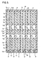
- circuit board area As further illustrated in FIGS. 4 and 5, is in the FPC on the film board according to the invention at least a circuit board area, according to the figurative representation however, preferably a plurality of board areas 5a, 5b, 5c, 5d, each as an electrical connection line educated.
- the weakening lines 6a, 6b, 6c, 6d may be involved here with advantage - as shown - around perforation lines act by simply punching in the invention Foil PCB can be introduced. alternative but it would also be possible, for example, with advantage, the Lines of weakness 6a, 6b, 6c, 6d by scribing the composite from carrier film 1 and cover layer 3 (scratches of carrier film 1 and / or cover layer 3).
- circuit board areas 5e, 5f, 5g, 5h, with each one as Connecting line formed circuit board area 5a, 5b, 5c, 5d connected via the lines of weakness 6a, 6b, 6c, 6d is to PCB areas, which for attachment to a Component, such as a motor vehicle body part determined are. But it could also be two trained as a connection line Areas 5a, 5b, 5c, 5d - over lines of weakness 6a, 6b, 6c, 6d connected - lie next to each other.
- FIGS. 4 and 5 it may advantageously be provided that through the conductor tracks 2 two or more circuits or FPC are formed, the via at least one in the carrier film 1 and / or in the Cover layer 3 arranged weakening line connected to each other are.
- FIGS. 4 and 5 are six similar FPCs A, B, C, D, E, F formed, which are each covered by lines of weakness, which are designated by the reference numerals 7 to 12. Also at these lines of weakness 7, 8, 9, 10, 11, 12 it can For example - as shown - perforation lines or act around scratched lines.
- Foil printed circuit board referred to as benefits, wherein a such benefits, even several dissimilar circuits for attachment to one or more component (s), e.g. a motor vehicle body could include.
- the production of a foil printed circuit board initially comprises the following process steps: laminating an electrical conductor layer on the carrier film 1, Printing a conductor pattern on the conductor layer, development the conductor tracks 2 of the circuit pattern by etching the conductor layer and applying the cover layer 3 (by film lamination or paint application) on the composite of carrier film 1 and circuit traces 2.
- the cover layer 3 by film lamination or paint application
- According to the method of Invention are then - after the application of the cover layer 3 - in the composite of carrier film 1 and cover layer 3, in particular by perforating or scribing, between the each formed as a connecting line circuit board area 5a, 5b, 5c, 5d and one or more other circuit board areas respective lines of weakness 6a, 6b, 6c, 6d brought in.
- connection line circuit board area 5a, 5b, 5c, 5d can after applying the Cover layer 3 and in particular after the introduction of the Lines of weakness 6a, 6b, 6c, 6d, 7, 8, 9, 10, 11, 12, in FIG an end portion which is about the size of a plug part corresponds to, cut out of the film board and, in particular by means of a crimping machine, with a Plug part 13a, 13b, 13c, 13d be assembled.
- FIG. 5 shows a foil circuit board according to the invention This manufacturing step, in each case at a free End of the formed as a connection line circuit board areas 5a, 5b, 5c, 5d a plug part 13a, 13b, 13c, 13d is attached.
- the FPC manufacturing process can advantageously from Roll to roll, that is, the carrier sheet 1 including the conductor layer as a roller conveyor 14 (see FIG. 4), each before printing the circuit pattern, before the development of the conductor 2, before the Applying the cover layer 3 and before the assembly rolled up and after each printing of the circuit diagram, after the development of the conductor tracks 2 and after insertion the weakening lines 6a, 6b, 6c, 6d, 7, 8, 9, 10, 11, 12 rolled up and after finishing in bows (Benefit) is cut. Before cutting can with Advantage still made a quality inspection.
- Such, equipped with connectors 13a, 13, 13c, 13c, 13d and tailored utility as shown in FIG. 5 may be, for example the dimensions are 600 mm x 1500 mm and is ready to ship, where it is flat and space saving for shipping can be packed in boxes.
- FIGS. 6 and 7 The assembly method according to the invention for an inventive Sheet-printed circuit board is illustrated by FIGS. 6 and 7 and comprises the method steps: fastening the film circuit board (only in Figs. 6 and 7 with the Reference numeral 15 denotes) on a component 16 - in the shown, as a variant, for example, according to FIG. 4 and 5 conceived embodiment of a mold heaven of an automobile and contacting each formed as a connection line Printed circuit board areas (in Fig. 7 with the reference numerals 5i, 5j, 5k, 5l, 5m, 5n and 5o) each of an electrical connection point.
- each remains as a connection line formed circuit board area 5i, 5j, 5k, 5l, 5m, 5n, 5o until after fixing the foil circuit board 15 on the component 16 via the in the composite of carrier film 1 and cover layer 3 arranged weakening lines (In unspecified in FIGS. 6 and 7) with one or connected to several other PCB areas.
- weakening lines In unspecified in FIGS. 6 and 7.
- Fig. 7 these printed circuit board areas 5i, 5j, 5k, 5l, 5m, 5n, 5o at the lines of weakness of the Foil PCB off or separated from it, to the each electrical connection point out and there contacted.
- the film conductor plate 15 according to the invention can with the Component 16 are glued for fastening in particular.
- a double-sided hybrid adhesive tape be used, this first with an adhesive side is glued to the component 16 and wherein then the Bonding the film circuit board 15 with the other adhesive side he follows.
- a such particularly suitable tape is in full Scope of the German utility model application 299 22 Directed to 805.3.
- the invention is not limited to the described Embodiment, but also includes all in the context of Invention, as claimed, equivalent embodiments. This is the case, for example also within the scope of the invention, if, as in German Utility Model Application 299 16 367.9 has been, in an end portion of the as a connecting line trained PCB area after application the cover layer of the circuit itself, in particular by folding, a plug part is formed.
- the film conductor plate 15 according to the invention can with the Component 16 for fastening alternatively to the described Bonding also ultrasonically welded or over Velcro band are connected.
Landscapes
- Engineering & Computer Science (AREA)
- Microelectronics & Electronic Packaging (AREA)
- Structure Of Printed Boards (AREA)
- Non-Metallic Protective Coatings For Printed Circuits (AREA)
- Printing Elements For Providing Electric Connections Between Printed Circuits (AREA)
- Laminated Bodies (AREA)
Description
- Fig. 1
- eine erste Variante des Aufbaus einer flexiblen gedruckten Schaltung (FPC) auf einer erfindungs gemäßen Folienleiterplatte, im Querschnitt, in einem Bereich entlang Linie I-I in Fig. 4,
- Fig. 2
- die erste Variante des Aufbaus einer flexiblen gedruckten Schaltung (FPC) auf einer erfindungsgemäßen Folienleiterplatte, im Querschnitt, in einem Bereich entlang Linie II-II in Fig. 4,
- Fig. 3
- in einer Fig. 1 entsprechenden Darstellung eine zweite Variante des Aufbaus einer flexiblen gedruckten Schaltung (FPC) auf einer erfindungsgemäßen Folienleiterplatte, im Querschnitt, in einem Bereich entlang Linie I-I in Fig. 4,
- Fig. 4
- eine Draufsicht auf eine erfindungsgemäße Folienleiterplatte,
- Fig. 5
- eine Draufsicht auf eine erfindungsgemäße Folienleiterplatte, in einer späteren Fertigungsstufe als in Fig. 4,
- Fig. 6
- die exemplarische Veranschaulichung eines Montageschrittes einer erfindungsgemäßen Folienleiterplatte,
- Fig. 7
- die exemplarische Veranschaulichung eines weiteren Montageschrittes einer erfindungsgemäßen Folienleiterplatte.
| Trägerfolie 1 | 50 µm |
| obere Kleberschicht 4a (Fig. 1, 2) | 25 µm |
| Leiterzüge 2 (Kupferfolie) | 70 µm |
| untere Kleberschicht 4b (Fig. 1, 2) | 35 µm |
| Deckfolie (Deckschicht 3 - Fig. 1) | 50 µm |
| Decklack (Deckschicht 3 - Fig. 3) | 30 µm |
- 1
- Trägerfolie
- 2
- Leiterzug
- 3
- Deckschicht
- 4
- Klebeverbindung (zwischen 1 und 2 bzw. 2 und 3)
- 4a
- Klebeverbindung zwischen 2 und 3
- 4b
- Klebeverbindung zwischen 1 und 2
- 5a-5d
- Anschlußleitungs-Leiterplattenbereiche
- 5e-5h
- Leiterplattenbereiche
- 5i-5o
- Anschlußleitungs-Leiterplattenbereiche
- 6a-6d
- Schwächungslinien bei 5a-5d
- 7-12
- Schwächungslinien bei A-F
- 13a-13d
- Stecker für 5a-5d
- 14
- Rollenbahn
- 15
- Folienleiterplatte (nur Fig. 6 und 7)
- 16
- Bauteil
- 17
- Zwischensteg
- 18
- Randsteg
- A-F
- Einzel-FPC im Nutzen
Claims (23)
- Folienleiterplatte(15), mit mindestens einer Trägerfolie (1), auf der elektrische Leiterzüge (2) angeordnet sind, welche durch mindestens eine mit der Trägerfolie (1) und den Leiterzügen (2) verbundene Deckschicht (3) abgedeckt sind, wodurch mindestens eine flexible gedruckte Schaltung (A-F) aufgebaut ist, in der mindestens ein Leiterplattenbereich (5a-5d, 5i-5o) als Anschlußleitung ausgebildet ist, wobei der als Anschlußleitung ausgebildete Leiterplattenbereich (5a-5d, 5i-5o) über mindestens eine in dem Verbund von Trägerfolie (1) und Deckschicht (3) angeordnete Schwächungslinie (6a-6d) mit einem oder mehreren anderen Leiterplattenbereichen (5e-5h, 17, 18) verbunden ist,
dadurch gekennzeichnet, daß die Trägerfolie (1) einschließlich der Leiterzüge (2) und der Deckschicht (3) als Rollenbahn (14) ausgeführt ist, in der mehrere, in Bögen (Nutzen) angeordnete, über mindestens eine Schwächungslinie (7-12) verbundene, manuell voneinander trennbare, flexible gedruckte Schaltungen (A-F) angeordnet sind. - Folienleiterplatte nach Anspruch 1,
dadurch gekennzeichnet, daß mehrere Leiterplattenbereiche (5a-5d, 5i-5o) als Anschlußleitungen ausgebildet sind. - Folienleiterplatte nach Anspruch 1 oder 2,
dadurch gekennzeichnet, daß ein Leiterplattenbereich, mit dem jeweils der als Anschlußleitung ausgebildete Leiterplattenbereich (5a-5d, 5i-5o) über die Schwächungslinie (6a-6d) verbunden ist, ein weiterer als Anschlußleitung ausgebildeter Leiterplattenbereich (5a - 5d, 5i-5o) ist. - Folienleiterplatte nach einem der Ansprüche 1 bis 3,
dadurch gekennzeichnet, daß ein Leiterplattenbereich (5e-5h), mit dem jeweils der als Anschlußleitung ausgebildete Leiterplattenbereich (5a-5d, 5i-5o) über die Schwächungslinie (6a-6d) verbunden ist, ein zur Befestigung an einem Bauteil, wie einem Kraftfahrzeug-Karosserieteil, bestimmter Leiterplattenbereich ist. - Folienleiterplatte nach einem der Ansprüche 1 bis 4,
dadurch gekennzeichnet, daß die Trägerfolie (1), die Leiterzüge (2) und die Deckschicht (3) über Klebeverbindungen (4, 4a, 4b) verbunden sind. - Folienleiterplatte nach einem der Ansprüche 1 bis 5,
dadurch gekennzeichnet, daß die Deckschicht (3) aus einer Deckfolie besteht. - Folienleiterplatte nach einem der Ansprüche 1 bis 5,
dadurch gekennzeichnet, daß die Deckschicht (3) aus einem flexiblen Decklack besteht. - Folienleiterplatte nach einem der Ansprüche 1 bis 7,
dadurch gekennzeichnet, daß an einem freien Ende des als Anschlußleitung ausgebildeten Leiterplattenbereiches (5a-5d, 5i-5o) ein Steckerteil (13a-13d) befestigt ist. - Folienleiterplatte nach einem der Ansprüche 1 bis 8,
dadurch gekennzeichnet, daß die Schwächungslinie(n) (6a-6d, 7-12), über die jeweils der als Anschlußleitung ausgebildete Leiterplattenbereich (5a-5d, 5i-5o) mit einem oder mehreren anderen Leiterplattenbereichen (5e-5h, 17, 18) verbunden ist und/oder über die mindestens zwei flexible gedruckte Schaltungen (A-F) miteinander verbunden sind, eine Perforationslinie ist. - Folienleiterplatte nach einem der Ansprüche 1 bis 8,
dadurch gekennzeichnet, daß die Schwächungslinie (6a-6d, 7-12), über die jeweils der als Anschlußleitung ausgebildete Leiterplattenbereich (5a-5d, 5i-5o) mit einem oder mehreren anderen Leiterplattenbereichen (5e-5h) verbunden ist und/oder über die mindestens zwei flexible gedruckte Schaltungen (A-F) miteinander verbunden sind, eine geritzte Linie ist. - Folienleiterplatte nach Anspruch 9,
dadurch gekennzeichnet, daß innerhalb einer als Perforationslinie ausgebildeten Schwächungslinie (7-12), über die mindestens zwei Schaltkreise bzw. flexible gedruckte Schaltungen (A-F) miteinander verbunden sind, alternierend kurze stegartige Verbindungsabschnitte und um ein Mehrfaches längere Schlitzabschnitte angeordnet sind. - Folienleiterplatte nach einem der Ansprüche 1 bis 11,
dadurch gekennzeichhnet, daß ein Leiterplattenbereich (5e-5h, 17, 18), mit dem jeweils der als Anschlußleitung ausgebildete Leiterplattenbereich (5a-5d, 5i-5o) über die Schwächungslinie (6a-6d, 7-12) verbunden ist, ein Zwischensteg (17) oder ein Randsteg (18) ist. - Verfahren zur Herstellung einer Folienleiterplatte (15), mit mindestens einer Trägerfolie (1), auf der elektrische Leiterzüge (2) angeordnet sind, welche durch mindestens eine mit der Trägerfolie (1) und den Leiterzügen (2) verbundene Deckschicht (3) abgedeckt sind, wodurch mindestens eine flexible gedruckte Schaltung (A-F) aufgebaut ist, in der mindestens ein Leiterplattenbereich (5a-5d, 5i-5o) als Anschlußleitung ausgebildet ist, umfassend die Verfahrenschritte: Laminieren einer elektrischen Leiterschicht auf die Trägerfolie (1), Erzeugung eines Leiterbildes und Aufbringen der Deckschicht (3) auf den Verbund aus Trägerfolie (1) und Leiterzügen (2), wobei nach dem Aufbringen der Deckschicht (3) in dem Verbund von Trägerfolie (1) und Deckschicht (3) zwischen den als Anschlußleitung ausgebildeten Leiterplattenbereich (5a-5d, 5i-5o) und einen oder mehrere andere Leiterplattenbereiche (5e-5h) mindestens eine Schwächungslinie (6a-6d) eingebracht wird, und gegebenenfalls der mindestens eine als Anschlußleitung ausgebildeten Leiterplattenbereich (5a-5d, 5i-5o) mit einem Steckerteil (13a-13d) konfektioniert wird,
dadurch gekennzeichnet, daß die Trägerfolie (1) einschließlich der Leiterschicht als Rollenbahn (14) eingesetzt wird, die jeweils vor dem Drucken des Leiterbildes, vor der Entwicklung der Leiterzüge (2), vor dem Aufbringen der Deckschicht (3) und gegebenenfalls dem Konfektionieren aufgerollt und jeweils nach dem Drucken des Leiterbildes, nach der Entwicklung der Leiterzüge (2) und nach dem Einbringen der Schwächungslinien (6a, 6b, 6c, 6d, 7, 8, 9, 10, 11, 12) eingerollt sowie danach und gegebenenfalls nach dem Konfektionieren in Bögen (Nutzen) getrennt wird. - Verfahren nach Anspruch 13,
dadurch gekennzeichnet, daß durch die Erzeugung des Leiterbildes, insbesondere durch ein Drucken des Leiterbildes und eine Entwicklung der Leiterzüge (2) durch Ätzen, zwei oder mehr flexible gedruckte Schaltungen (A-F) gebildet werden und nach dem Aufbringen der Deckschicht (3) in den Verbund von Trägerfolie (1) und Deckschicht (3) zwischen diese Schaltungen (A-F) mindestens eine Schwächungslinie (7-12) eingebracht wird. - Verfahren nach Anspruch 13 oder 14,
dadurch gekennzeichnet, daß der Verbund von Trägerfolie (1) und Deckschicht (3) zur Herstellung der Schwächungslinie(n) (6a-6d, 7-12) perforiert wird. - Verfahren nach Anspruch 13 oder 14,
dadurch gekennzeichnet, daß der Verbund von Trägerfolie (1) und Deckschicht (3) zur Herstellung der Schwächungslinie(n) (6a-6d, 7-12) geritzt wird. - Verfahren nach einem der Ansprüche 13 bis 16,
dadurch gekennzeichnet, daß der als Anschlußleitung ausgebildete Leiterplattenbereich (5a-5d, 5i-5o) nach dem Aufbringen der Deckschicht (3) in einem Endabschnitt, der etwa der Größe eines Steckerteiles (13a-13d) entspricht, aus der Folienleiterplatte herausgetrennt und mit einem Steckerteil (13a-13d) konfektioniert wird. - Verfahren nach einem der Ansprüche 13 bis 16,
dadurch gekennzeichnet, daß in einem Endabschnitt des als Anschlußleitung ausgebildeten Leiterplattenbereiches (5a-5d, 5i-5o) nach dem Aufbringen der Deckschicht (3) aus der Schaltung selbst, insbesondere durch Faltung, ein Steckerteil gebildet wird. - Verfahren nach Anspruch 18,
dadurch gekennzeichnet, daß die Rollenbahn (14) vor der Bildung des Steckerteiles aufgerollt und danach in Bögen (Nutzen) geschnitten wird. - Verfahren nach einem der Ansprüche 17 bis 19,
dadurch gekennzeichnet, daß nach der Konfektionierung oder der Steckerbildung eine Qualitätsprüfung erfolgt. - Verfahren zur Montage einer Folienleiterplatte (15), mit mindestens einer Trägerfolie (1), auf der elektrische Leiterzüge (2) angeordnet sind, welche durch mindestens eine mit der Trägerfolie (1) und den Leiterzügen (2) verbundene Deckschicht (3) abgedeckt sind, wodurch mindestens eine flexible gedruckte Schaltung (A-F) aufgebaut ist, in der mindestens ein Leiterplattenbereich (5a-5d, 5i-5o) als Anschlußleitung ausgebildet ist, umfassend die Verfahrenschritte: Befestigen der Folienleiterplatte (15) an einem Bauteil (16) und kontaktierung der Anschlußleitung an mindestens einer elektrischen Anschlußstelle, wobei jeweils der als Anschlußleitung ausgebildete Leiterplattenbereich (5a-5d, 5i-5o) bis nach dem Befestigen der Folienleiterplatte (15) an dem Bauteil (16) über mindestens eine in dem Verbund von Trägerfolie (1) und Deckschicht (3) angeordnete Schwächungslinie (6a-6d) mit einem oder mehreren anderen Leiterplattenbereichen (5e-5h, 17, 18) verbunden bleibt, und anschließend an der Schwächungslinie (6d-6e) von der Folienleiterplatte (15) ab- oder daraus herausgetrennt, zu der jeweiligen elektrischen Anschlußstelle geführt und dort kontaktiert wird,
dadurch gekennzeichnet, daß vor dem Befestigen der Folienleiterplatte (15) an dem Bauteil (16) zwei oder mehr flexible gedruckte Schaltungen (A-F), die über mindestens eine in dem Verbund von Trägerfolie (1) und Deckschicht (3) angeordnete Schwächungslinie (7-12) untereinander in einem Bogen (Nutzen) in einer Rollenbahn (14) verbunden sind, an der Schwächungslinie (7-12) voneinander gelöst werden. - Verfahren nach Anspruch 21,
dadurch gekennzeichnet, daß die Folienleiterplatte (15) mit dem Bauteil (16) zum Befestigen verklebt, ultraschallverschweißt oder mittels eines Klettbandes verbunden wird. - Verfahren nach Anspruch 22,
dadurch gekennzeichnet, daß zum Verkleben ein doppelseitiges Hybridklebeband eingesetzt wird.
Applications Claiming Priority (2)
| Application Number | Priority Date | Filing Date | Title |
|---|---|---|---|
| DE10031940A DE10031940A1 (de) | 2000-06-30 | 2000-06-30 | Folienleiterplatte sowie deren Herstellungs- und Montageverfahren |
| DE10031940 | 2000-06-30 |
Publications (3)
| Publication Number | Publication Date |
|---|---|
| EP1168897A2 EP1168897A2 (de) | 2002-01-02 |
| EP1168897A3 EP1168897A3 (de) | 2004-01-02 |
| EP1168897B1 true EP1168897B1 (de) | 2005-08-17 |
Family
ID=7647381
Family Applications (1)
| Application Number | Title | Priority Date | Filing Date |
|---|---|---|---|
| EP01112929A Expired - Lifetime EP1168897B1 (de) | 2000-06-30 | 2001-06-06 | Folienleiterplatte sowie deren Herstellungs- und Montageverfahren |
Country Status (4)
| Country | Link |
|---|---|
| EP (1) | EP1168897B1 (de) |
| AT (1) | ATE302541T1 (de) |
| DE (2) | DE10031940A1 (de) |
| ES (1) | ES2243364T3 (de) |
Families Citing this family (5)
| Publication number | Priority date | Publication date | Assignee | Title |
|---|---|---|---|---|
| DE20108532U1 (de) * | 2001-05-21 | 2001-09-13 | Coroplast Fritz Müller GmbH & Co. KG, 42279 Wuppertal | Folienleiter, wie Folienleiterkabel oder -platte |
| DE20204011U1 (de) | 2002-03-13 | 2002-07-04 | Coroplast Fritz Müller GmbH & Co. KG, 42279 Wuppertal | Elektrische Verbindungsanordnung mit einer Folienleiterplatte oder einem Folienleiterkabel sowie elektrisches Brückenelement und Verarbeitungseinheit für diese Anordnung |
| US8895864B2 (en) * | 2012-03-30 | 2014-11-25 | Nokia Corporation | Deformable apparatus and method |
| EP2991460B1 (de) | 2014-08-29 | 2018-11-21 | Nokia Technologies OY | Vorrichtung und zugehörige Verfahren für verformbare Elektronik |
| CN113038696B (zh) * | 2021-03-02 | 2022-06-14 | 广德新三联电子有限公司 | 一种汽车用高耐弯性电路板及其制备方法 |
Family Cites Families (9)
| Publication number | Priority date | Publication date | Assignee | Title |
|---|---|---|---|---|
| FR2283528A1 (fr) * | 1974-08-30 | 1976-03-26 | Reinshagen Kabelwerk Gmbh | Connexion omnibus de cables et procede pour sa fabrication |
| DE3922121A1 (de) * | 1989-07-05 | 1991-01-17 | Siemens Ag | Flexible leiterplatte zur herstellung elektrischer verbindungen |
| JP2847246B2 (ja) * | 1989-08-31 | 1999-01-13 | 日本メクトロン株式会社 | 可撓性回路基板集合体及びその製造法 |
| JPH04171786A (ja) * | 1990-11-02 | 1992-06-18 | Sumitomo Wiring Syst Ltd | フレキシブル配線基板ケーブル |
| JP2586971B2 (ja) * | 1991-11-06 | 1997-03-05 | 帝国通信工業株式会社 | フレキシブル基板付き電子部品 |
| DE19651863A1 (de) * | 1996-12-13 | 1998-06-18 | Bosch Gmbh Robert | Anzeigevorrichtung |
| JPH09181401A (ja) * | 1997-02-13 | 1997-07-11 | Sumitomo Wiring Syst Ltd | フレキシブルプリント配線板の使用方法 |
| DE19720167B4 (de) * | 1997-05-14 | 2006-06-22 | Siemens Ag | Struktur zum Anschließen einer Mehrzahl voneinander entfernter elektrischer Bauelemente an eine Zentraleinheit |
| JP4144085B2 (ja) * | 1998-11-27 | 2008-09-03 | 松下電器産業株式会社 | 携帯型電子機器 |
-
2000
- 2000-06-30 DE DE10031940A patent/DE10031940A1/de not_active Withdrawn
-
2001
- 2001-06-06 DE DE50107097T patent/DE50107097D1/de not_active Expired - Fee Related
- 2001-06-06 ES ES01112929T patent/ES2243364T3/es not_active Expired - Lifetime
- 2001-06-06 AT AT01112929T patent/ATE302541T1/de not_active IP Right Cessation
- 2001-06-06 EP EP01112929A patent/EP1168897B1/de not_active Expired - Lifetime
Also Published As
| Publication number | Publication date |
|---|---|
| DE10031940A1 (de) | 2002-01-10 |
| EP1168897A3 (de) | 2004-01-02 |
| DE50107097D1 (de) | 2005-09-22 |
| ES2243364T3 (es) | 2005-12-01 |
| ATE302541T1 (de) | 2005-09-15 |
| EP1168897A2 (de) | 2002-01-02 |
Similar Documents
| Publication | Publication Date | Title |
|---|---|---|
| EP0756244B1 (de) | Schaltungseinheit und Verfahren zur Herstellung einer Schaltungseinheit | |
| DE69812039T2 (de) | Herstellungsverfahren für eine transponderspule | |
| DE19819088B4 (de) | Flexible Leiterplatte | |
| EP1162631B1 (de) | Stecker zur Kontaktierung eines Flachbandkabels | |
| DE3411973A1 (de) | Plattenmaterial zur herstellung flexibler gedruckter schaltungstraeger, verfahren zur herstellung flexibler gedruckter schaltungstraeger und nach diesem verfahren hergestellter flexibler gedruckter schaltungstraeger | |
| EP1168897B1 (de) | Folienleiterplatte sowie deren Herstellungs- und Montageverfahren | |
| EP4184530A1 (de) | Kabelsatz sowie verfahren zur herstellung eines kabelsatzes | |
| DE10103761A1 (de) | Flexibles Flachbandkabel | |
| EP1263269B1 (de) | Folienleiter, wie Folienleiterkabel oder -platte | |
| DE20013651U1 (de) | Folienleiterplatte | |
| DE19601899C1 (de) | Fördergurt mit eingebetteten Leiterschleifen | |
| DE2741025A1 (de) | Flaechenheizelement und verfahren zu seiner herstellung | |
| DE20204011U1 (de) | Elektrische Verbindungsanordnung mit einer Folienleiterplatte oder einem Folienleiterkabel sowie elektrisches Brückenelement und Verarbeitungseinheit für diese Anordnung | |
| DE102010054974A1 (de) | Leiterplatte und Verfahren zur Herstellung von Leiterplatten | |
| DE10020761B4 (de) | Folienleiter sowie Verfahren zur Herstellung eines Folienleiters | |
| DE19855023A1 (de) | Verfahren und Vorrichtung zum Aufbringen einer flexiblen Leiterbahn auf eine beliebig geformte Oberfläche | |
| EP3111735B1 (de) | Folienverbund mit elektrischer funktionalität zum aufbringen auf ein substrat | |
| EP1349182B1 (de) | Verfahren zur Herstellung einer Flachleiter-Bandleitung | |
| DE102019114148B4 (de) | Verfahren zum Herstellen einer flächigen Elektronikanordnung, Elektronikanordnung und Luftfahrzeug mit einer flächigen Elektronikanordnung | |
| DE20014701U1 (de) | Selbstklebendes elektrisches oder optisches Kabel | |
| EP1808058A1 (de) | Verfahren zur herstellung einer dreidimensionalen schaltung | |
| EP0653743B1 (de) | Verfahren zur Herstellung eines Isolierelementes | |
| EP2621252A2 (de) | Flexibler elektrischer Verbinder | |
| WO1995026123A1 (de) | Verfahren zur herstellung von folienleiterplatten oder halbzeugen für folienleiterplatten | |
| DE102016226257A1 (de) | Mehrlagige leiterkarte und verfahren zum herstellen einer solchen mehrlagigen leiterkarte |
Legal Events
| Date | Code | Title | Description |
|---|---|---|---|
| PUAI | Public reference made under article 153(3) epc to a published international application that has entered the european phase |
Free format text: ORIGINAL CODE: 0009012 |
|
| AK | Designated contracting states |
Kind code of ref document: A2 Designated state(s): AT BE CH CY DE DK ES FI FR GB GR IE IT LI LU MC NL PT SE TR |
|
| AX | Request for extension of the european patent |
Free format text: AL;LT;LV;MK;RO;SI |
|
| PUAL | Search report despatched |
Free format text: ORIGINAL CODE: 0009013 |
|
| AK | Designated contracting states |
Kind code of ref document: A3 Designated state(s): AT BE CH CY DE DK ES FI FR GB GR IE IT LI LU MC NL PT SE TR |
|
| AX | Request for extension of the european patent |
Extension state: AL LT LV MK RO SI |
|
| 17P | Request for examination filed |
Effective date: 20040526 |
|
| AKX | Designation fees paid |
Designated state(s): AT BE CH CY DE DK ES FI FR GB GR IE IT LI LU MC NL PT SE TR |
|
| GRAP | Despatch of communication of intention to grant a patent |
Free format text: ORIGINAL CODE: EPIDOSNIGR1 |
|
| GRAS | Grant fee paid |
Free format text: ORIGINAL CODE: EPIDOSNIGR3 |
|
| GRAA | (expected) grant |
Free format text: ORIGINAL CODE: 0009210 |
|
| AK | Designated contracting states |
Kind code of ref document: B1 Designated state(s): AT BE CH CY DE DK ES FI FR GB GR IE IT LI LU MC NL PT SE TR |
|
| PG25 | Lapsed in a contracting state [announced via postgrant information from national office to epo] |
Ref country code: IE Free format text: LAPSE BECAUSE OF FAILURE TO SUBMIT A TRANSLATION OF THE DESCRIPTION OR TO PAY THE FEE WITHIN THE PRESCRIBED TIME-LIMIT Effective date: 20050817 Ref country code: FI Free format text: LAPSE BECAUSE OF FAILURE TO SUBMIT A TRANSLATION OF THE DESCRIPTION OR TO PAY THE FEE WITHIN THE PRESCRIBED TIME-LIMIT Effective date: 20050817 Ref country code: TR Free format text: LAPSE BECAUSE OF FAILURE TO SUBMIT A TRANSLATION OF THE DESCRIPTION OR TO PAY THE FEE WITHIN THE PRESCRIBED TIME-LIMIT Effective date: 20050817 Ref country code: NL Free format text: LAPSE BECAUSE OF FAILURE TO SUBMIT A TRANSLATION OF THE DESCRIPTION OR TO PAY THE FEE WITHIN THE PRESCRIBED TIME-LIMIT Effective date: 20050817 |
|
| REG | Reference to a national code |
Ref country code: GB Ref legal event code: FG4D Free format text: NOT ENGLISH |
|
| REG | Reference to a national code |
Ref country code: CH Ref legal event code: EP |
|
| REG | Reference to a national code |
Ref country code: IE Ref legal event code: FG4D Free format text: LANGUAGE OF EP DOCUMENT: GERMAN |
|
| REF | Corresponds to: |
Ref document number: 50107097 Country of ref document: DE Date of ref document: 20050922 Kind code of ref document: P |
|
| GBT | Gb: translation of ep patent filed (gb section 77(6)(a)/1977) |
Effective date: 20050912 |
|
| PG25 | Lapsed in a contracting state [announced via postgrant information from national office to epo] |
Ref country code: SE Free format text: LAPSE BECAUSE OF FAILURE TO SUBMIT A TRANSLATION OF THE DESCRIPTION OR TO PAY THE FEE WITHIN THE PRESCRIBED TIME-LIMIT Effective date: 20051117 Ref country code: GR Free format text: LAPSE BECAUSE OF FAILURE TO SUBMIT A TRANSLATION OF THE DESCRIPTION OR TO PAY THE FEE WITHIN THE PRESCRIBED TIME-LIMIT Effective date: 20051117 Ref country code: DK Free format text: LAPSE BECAUSE OF FAILURE TO SUBMIT A TRANSLATION OF THE DESCRIPTION OR TO PAY THE FEE WITHIN THE PRESCRIBED TIME-LIMIT Effective date: 20051117 |
|
| REG | Reference to a national code |
Ref country code: ES Ref legal event code: FG2A Ref document number: 2243364 Country of ref document: ES Kind code of ref document: T3 |
|
| PG25 | Lapsed in a contracting state [announced via postgrant information from national office to epo] |
Ref country code: PT Free format text: LAPSE BECAUSE OF FAILURE TO SUBMIT A TRANSLATION OF THE DESCRIPTION OR TO PAY THE FEE WITHIN THE PRESCRIBED TIME-LIMIT Effective date: 20060117 |
|
| NLV1 | Nl: lapsed or annulled due to failure to fulfill the requirements of art. 29p and 29m of the patents act | ||
| REG | Reference to a national code |
Ref country code: IE Ref legal event code: FD4D |
|
| ET | Fr: translation filed | ||
| PLBE | No opposition filed within time limit |
Free format text: ORIGINAL CODE: 0009261 |
|
| STAA | Information on the status of an ep patent application or granted ep patent |
Free format text: STATUS: NO OPPOSITION FILED WITHIN TIME LIMIT |
|
| PG25 | Lapsed in a contracting state [announced via postgrant information from national office to epo] |
Ref country code: LI Free format text: LAPSE BECAUSE OF NON-PAYMENT OF DUE FEES Effective date: 20060630 Ref country code: CH Free format text: LAPSE BECAUSE OF NON-PAYMENT OF DUE FEES Effective date: 20060630 Ref country code: MC Free format text: LAPSE BECAUSE OF NON-PAYMENT OF DUE FEES Effective date: 20060630 Ref country code: BE Free format text: LAPSE BECAUSE OF NON-PAYMENT OF DUE FEES Effective date: 20060630 |
|
| 26N | No opposition filed |
Effective date: 20060518 |
|
| REG | Reference to a national code |
Ref country code: CH Ref legal event code: PL |
|
| PG25 | Lapsed in a contracting state [announced via postgrant information from national office to epo] |
Ref country code: AT Free format text: LAPSE BECAUSE OF NON-PAYMENT OF DUE FEES Effective date: 20060606 |
|
| BERE | Be: lapsed |
Owner name: COROPLAST FRITZ MULLER G.M.B.H. & CO. KG Effective date: 20060630 |
|
| PG25 | Lapsed in a contracting state [announced via postgrant information from national office to epo] |
Ref country code: LU Free format text: LAPSE BECAUSE OF NON-PAYMENT OF DUE FEES Effective date: 20060606 |
|
| PG25 | Lapsed in a contracting state [announced via postgrant information from national office to epo] |
Ref country code: CY Free format text: LAPSE BECAUSE OF FAILURE TO SUBMIT A TRANSLATION OF THE DESCRIPTION OR TO PAY THE FEE WITHIN THE PRESCRIBED TIME-LIMIT Effective date: 20050817 |
|
| PGFP | Annual fee paid to national office [announced via postgrant information from national office to epo] |
Ref country code: ES Payment date: 20090610 Year of fee payment: 9 |
|
| PGFP | Annual fee paid to national office [announced via postgrant information from national office to epo] |
Ref country code: IT Payment date: 20090624 Year of fee payment: 9 |
|
| PGFP | Annual fee paid to national office [announced via postgrant information from national office to epo] |
Ref country code: DE Payment date: 20090825 Year of fee payment: 9 Ref country code: GB Payment date: 20090603 Year of fee payment: 9 |
|
| GBPC | Gb: european patent ceased through non-payment of renewal fee |
Effective date: 20100606 |
|
| REG | Reference to a national code |
Ref country code: FR Ref legal event code: ST Effective date: 20110228 |
|
| PG25 | Lapsed in a contracting state [announced via postgrant information from national office to epo] |
Ref country code: IT Free format text: LAPSE BECAUSE OF NON-PAYMENT OF DUE FEES Effective date: 20100606 |
|
| PG25 | Lapsed in a contracting state [announced via postgrant information from national office to epo] |
Ref country code: DE Free format text: LAPSE BECAUSE OF NON-PAYMENT OF DUE FEES Effective date: 20110101 |
|
| PG25 | Lapsed in a contracting state [announced via postgrant information from national office to epo] |
Ref country code: FR Free format text: LAPSE BECAUSE OF NON-PAYMENT OF DUE FEES Effective date: 20100630 |
|
| PG25 | Lapsed in a contracting state [announced via postgrant information from national office to epo] |
Ref country code: GB Free format text: LAPSE BECAUSE OF NON-PAYMENT OF DUE FEES Effective date: 20100606 |
|
| REG | Reference to a national code |
Ref country code: ES Ref legal event code: FD2A Effective date: 20111118 |
|
| PG25 | Lapsed in a contracting state [announced via postgrant information from national office to epo] |
Ref country code: ES Free format text: LAPSE BECAUSE OF NON-PAYMENT OF DUE FEES Effective date: 20100607 |
|
| PGFP | Annual fee paid to national office [announced via postgrant information from national office to epo] |
Ref country code: FR Payment date: 20090611 Year of fee payment: 9 |