EP1186898A2 - Verfahren und Vorrichtung zum Prüfen von Leiterplatten - Google Patents
Verfahren und Vorrichtung zum Prüfen von Leiterplatten Download PDFInfo
- Publication number
- EP1186898A2 EP1186898A2 EP01119256A EP01119256A EP1186898A2 EP 1186898 A2 EP1186898 A2 EP 1186898A2 EP 01119256 A EP01119256 A EP 01119256A EP 01119256 A EP01119256 A EP 01119256A EP 1186898 A2 EP1186898 A2 EP 1186898A2
- Authority
- EP
- European Patent Office
- Prior art keywords
- circuit board
- test points
- printed circuit
- board test
- testing
- Prior art date
- Legal status (The legal status is an assumption and is not a legal conclusion. Google has not performed a legal analysis and makes no representation as to the accuracy of the status listed.)
- Granted
Links
Images



Classifications
-
- G—PHYSICS
- G01—MEASURING; TESTING
- G01R—MEASURING ELECTRIC VARIABLES; MEASURING MAGNETIC VARIABLES
- G01R31/00—Arrangements for testing electric properties; Arrangements for locating electric faults; Arrangements for electrical testing characterised by what is being tested not provided for elsewhere
- G01R31/28—Testing of electronic circuits, e.g. by signal tracer
- G01R31/2801—Testing of printed circuits, backplanes, motherboards, hybrid circuits or carriers for multichip packages [MCP]
- G01R31/2806—Apparatus therefor, e.g. test stations, drivers, analysers, conveyors
Definitions
- the invention relates to a method and a device for testing printed circuit boards, especially for testing bare printed circuit boards.
- PCB test points have a large number of networks, the density of which varies continuously with the continuing miniaturization of electronic components is increasing.
- the density of the contact points on the printed circuit boards also increases in a corresponding manner, hereinafter referred to as PCB test points.
- Known devices for the electrical testing of printed circuit boards can basically be divided into two groups.
- the first group is the parallel tester shown, which have an adapter with which all circuit board test points to be scanned PCB can be contacted simultaneously.
- the second Group includes the sequential testers. This particularly includes the finger testers. These are devices with two or more contact fingers each Scan PCB test points sequentially.
- Finger testers are, for example, from DE 41 09 684 A1 and EP 0 468 153 A1 known. Finger testers have a high degree of flexibility, because when changing the one to be tested PCB type no mechanical changes can be made have to. Finger testers scan the individual circuit board test points sequentially with their test fingers from. The contact fingers can with an accuracy of e.g. 5 ⁇ m be positioned. Depending on the design of the contact fingers, however, two contact fingers can be used not arbitrarily close together, so that two next to each other PCB test points with a center distance of less than 100 ⁇ m to 300 ⁇ m cannot be contacted at the same time.
- Test devices are also known for testing printed circuit boards, which are the circuit board test points make electrical contact with a plasma.
- the plasma will e.g. generated by means of a laser beam.
- Another way of contactless Contacting is using an electron beam. With this contactless working test equipment, it is problematic very close to each other contact lying test points. If you create two closely together lying plasma areas so there is a significant risk that the intermediate area is heated and ionized accordingly, whereby the two plasma areas would unite. This represents a short circuit which is a useful measurement makes impossible.
- PCB test points with e.g. to test a center distance of 100 ⁇ m to 300 ⁇ m.
- optical test methods and test devices are known (e.g. WO 92/09880, WO 93/15474).
- Such devices have an optical Scanner on, e.g. a camera with which a circuit board to be tested is scanned.
- the image of the printed circuit board determined in this way is digitized, i.e. that an image data file is created, the data content of which corresponds to the illustration.
- the image data file usually consists of a list of coordinates, each one Coordinate is assigned a gray value.
- This image data file is automatically created using read a recognition program that the individual conductor tracks, contact points and the like. Recognizes and stores them in a feature file in which all optical features the circuit board to be tested are included.
- This feature file is compared with a reference feature file. Become at this comparison found no deviations, so is the tested circuit board error-free. However, if deviations are found, this is an indication that the PCB to be tested has an error, e.g. a short circuit or an interruption in a network.
- optical test devices allow a very quick test of one layer Printed circuit board before assembling the individual layers into a printed circuit board. With Such test devices can be used to test different circuit boards, without mechanical changes to the device being necessary for this. On finished circuit boards, outer layers are tested with the optical test device.
- the invention has for its object to a method and an apparatus create with which simple and reliable circuit boards with high contact point density can be tested.
- circuit board test points are very difficult to scan electrically are arranged, are measured optically according to the invention. These areas are referred to below as scan areas. It is an advantage that the conductor tracks, which are adjacent and thus closely arranged Connect circuit board test points on the surface of the circuit board to be tested are trained. These conductor tracks can be captured optically. This tight PCB test points lying next to each other can be fully automated with high reliability be tested optically, since the areas to be optically evaluated in each case Small cutouts of the circuit boards to be tested are safe and easy can be evaluated automatically.
- the method according to the invention thus allows one in a simple manner reliable test of all circuit board test points of a circuit board to be tested.
- Electrical testing can be carried out using a parallel tester, finger tester, plasma, Laser or electron beam testers are used.
- FIG. 1 schematically shows a test device 1 according to the invention with a parallel tester 2 and an optical measuring station 3.
- the parallel tester 2 has a base body 4, on the top of which a receiving area 5 is designed for receiving a circuit board to be tested.
- the receiving area is provided with an adapter, the test needles as contact elements has, which simultaneously several PCB test points of the to be tested PCB can contact.
- Above the base body 4 is a pressure plate 6 arranged.
- the pressure plate 6 is vertical by means of a printing mechanism adjustable (double arrow 7).
- the pressure mechanism is shown schematically by a Pressure cylinder 8 shown.
- On the underside of the pressure plate 6 is opposite to the receiving area 5 another adapter with serving as contact elements Test needles arranged.
- the pressure plate 6 can be up to the top of the Base body 4 are lowered, so that a circuit board to be tested on both Sides with the two adapters is electrically contacted.
- the conveyor leads from one known separation station (not shown) in the conveying direction 10 for Parallel tester 2, to the optical measuring station 3 and to a collecting station known per se (not shown) for collecting the tested circuit boards.
- the optical measuring station 3 has a frame 11 on which gripping elements 12 are arranged to hold a circuit board to be tested.
- an upper camera 14 is attached by means of holding struts 13, with its lens on the area spanned by the frame 11 is aligned so that one in the frame 11 held circuit board can be completely scanned by the camera 14 can.
- a lower camera with additional holding struts 15 16 arranged, with their lens up on the spanned by the frame Area is directed so that a circuit board held in the frame is complete can be scanned by the lower camera 16.
- Both the parallel tester 2 and the optical measuring station 3 are equipped with a control device 17 connected, the parallel tester 2 and the optical measuring station 3 and control the conveyor.
- a circuit board to be tested is first moved into the receiving area by means of the conveyor 5 of the parallel tester 2 promoted. To test this circuit board the pressure plate 6 lowered so that circuit board test points on both sides of the PCB to be tested are electrically contacted by the two adapters. Then the circuit board in a conventional manner on interruptions and Short circuits tested. After testing, the pressure plate 6 is raised and the circuit board released again.
- the circuit board is transported to the optical measuring station and by means of the gripping elements 12 fixed in the frame 11.
- the top of the circuit board to be tested is by means of the upper camera 14 scanned and the bottom is by means of the lower Camera 16 scanned.
- the digital images generated in this way are evaluated, only scanning areas on the circuit board are evaluated. In the scanning areas there are at least two circuit board test points close together arranged and if these circuit board test points by means of conductor tracks with other Circuit board test points are connected, these are further circuit board test points arranged within the respective scanning area.
- These scan areas are once determined in advance and determined for the evaluation of the digital images. she usually only cover a small fraction of the total area testing circuit board. This fraction can e.g. are in the range of 3% to 10%.
- FIG. 4 schematically shows an area of a circuit board 19 to be tested in one Top view with a few PCB test points 20.
- a first group of PCB test points 20a, 20b and 20c are arranged adjacent to each other, wherein the circuit board test points 20a, 20b are electrically interconnected with a conductor track 21 are connected. Since this conductor track 21 has two adjacent circuit board test points 20a, 20b connects it is formed on the surface of the circuit board and can therefore be easily captured optically.
- Next to the circuit board test point 20b is the circuit board test point 20c. This circuit board test point 20c is not connected to any conductor track. At such individual circuit board test points connections of electrical components are only mechanical Attachment soldered to the circuit board. However, it must also be ensured be that these individual circuit board test points do not match another circuit board test point or a conductor track are electrically connected.
- the circuit board test points 20a, 20b and 20c lie within a scanning range 22 with predetermined radius r.
- the radius r of the scanning area 22 is, for example. 100 to 200 ⁇ m. However, it may also be expedient to reduce the radius r to 50 ⁇ m set.
- This circuit board has a second group of individual adjacent circuit board test points 20d, 20e which are within a further scanning area 22 lie. Since these two circuit board test points 20d, 20e are very close to each other are arranged, they can not be electrically at the same time without considerable effort and be contacted safely. The scanning area 22 is therefore optically therefor evaluated whether a short circuit between the two circuit board test points 20d, 20e is present.
- this circuit board has a third group of four circuit board test points 20f, which are arranged closely adjacent to each other. These four circuit board test points are electrically connected to one another in pairs by means of conductor tracks 21. There these units of conductor tracks 21 and circuit board test points 20f within one Scanning range 22 are, they are not electrically without considerable effort at the same time securely contactable, which is why it is based on an optical evaluation Short circuits and interruptions can be tested.
- all of the circuit board test points are thus and possibly traces of existing pairs of structures, each complete arranged within a scanning area with a predetermined radius r are by evaluating the optically recorded image for short circuit and interruption tested. These structures become electrical compared to the other structures tested for short circuit and all other structures are electrically open Short circuit and interruptions tested.
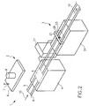
- Fig. 2 shows a second embodiment of the test device according to the invention.
- This embodiment again has a parallel tester 2 and an optical one Measuring station 3 on.
- the parallel tester 2 and the conveyor are identical to first embodiment, which is why the corresponding same parts are designated by the same reference numerals.
- the optical measuring station 3 has a base body 24, the upper side of which is one Receiving area 23 is designed for receiving a circuit board to be tested.
- the receiving area 23 is spanned by a cross member 27, which on the Base body 24 is movable in and against the conveying direction 10.
- a camera 25 arranged on the cross member 27 transversely to the transport direction 10 is movable, so that the traverse 27 is movable the base body 24 and the movability of the camera 25 on the cross member 27
- Camera 25 arranged above any position of the recording area 23 can be.
- the camera 25 is with its lens facing down towards the recording area 23 directed.
- the operation of the device shown in FIG. 2 corresponds to that shown in FIG. 1 Device, the camera 25 in each case over the optical testing Areas of the circuit board is positioned at which adjacent electrical PCB test points connected via a conductor track. Because the camera These areas can be arranged very close to the circuit board to be tested can be recorded very precisely and evaluated accordingly.
- the one shown in Fig. 2 The device only allows the optical scanning of one side of one to be tested PCB. This is often useful because there are many PCBs on one side of PCB test points have in very high density and on the other hand relative Few circuit board test points have a large distance from each other have. With such circuit boards, only the side with the in printed circuit board test points can be optically tested.
- FIG. 3 shows a further exemplary embodiment of a test device according to the invention 1, which is designed as a finger tester.
- This test device 1 has one Base body 24, on the top of which a receiving area 23 for receiving a circuit board to be tested is formed.
- the top of the body 24 is bounded on the long sides by a rail 26 each.
- On the rails 26 store two trusses 27 which are movable along the rail 26 (in the direction of the Double arrow 28).
- Contact fingers 29 are arranged on the traverses 27, which run along the traverses 27 are movable.
- the contact fingers 29 have at their free ends Contact tips 31 with which the circuit board test points one to be tested PCB can be contacted.
- a contact tip 31 for contacting a circuit board test point can be positioned.
- On the trusses 27 are each additional a camera 32 is arranged. The cameras 32 are in turn along the traverses 27 (in the direction of the double arrow 30), so that over any position of the recording area 23, a camera 32 can be positioned.
- the cameras 32 are each with their lenses facing downwards Recording area 23 directed.
- test device 1 The mode of operation of the test device 1 shown in FIG. 3 will be described in more detail below explained.
- circuit board test points that are electrically connected to each other over a greater distance scanned by the contact fingers 29 and measured electrically.
- optical measurements by means of the camera 32 and the electrical measurements by means of the contact fingers 29 can be carried out in any order.
- the advantages explained above are realized the combination of optical and electrical measurement methods.
- the essence of the invention is that an electrical and an optical measurement are combined in this way be that the closely spaced PCB test points are optically measured and other pairs of circuit board points that are electrically connected together are tested using an electrical measuring method.
- electrical measuring methods can touch contacts (parallel tester, finger tester) have or non-contact measurements (plasma, laser beam or electron beam method) To run.
Landscapes
- Engineering & Computer Science (AREA)
- Computer Hardware Design (AREA)
- Microelectronics & Electronic Packaging (AREA)
- General Engineering & Computer Science (AREA)
- Physics & Mathematics (AREA)
- General Physics & Mathematics (AREA)
- Tests Of Electronic Circuits (AREA)
- Testing Of Short-Circuits, Discontinuities, Leakage, Or Incorrect Line Connections (AREA)
- Measuring Leads Or Probes (AREA)
- Investigating Materials By The Use Of Optical Means Adapted For Particular Applications (AREA)
Abstract
- optisches Prüfen von Gruppen von Leiterplattentestpunkten und ggfs. von damit verbundenen Leiterbahnen innerhalb von Abtastbereichen mit vorbestimmten Radius, wobei die Gruppen von Leiterplattentestpunkte und Leiterbahnen jeweils vollständig innerhalb der Abtastbereiche angeordnet sind, und
- elektrisches Prüfen der übrigen Leiterplattentestpunkte und Leiterbahnen.
Description
- Bestimmen von Abtastbereichen, in denen jeweils eine Gruppe von eng nebeneinander liegenden Leiterplattentestpunkten angeordnet ist,
- optisches Prüfen auf Kurzschluss und Unterbrechung der Gruppen von Leiterplattentestpunkten und ggfs. von damit verbundenen Leiterbahnen innerhalb der Abtastbereiche, wobei die Gruppen von Leiterplattentestpunkte und Leiterbahnen jeweils vollständig innerhalb der Abtastbereiche angeordnet sind, und
- elektrisches Prüfen auf Kurzschluss und Unterbrechungen der übrigen Leiterplattentestpunkte und der übrigen Leiterbahnen.
- Fig.
- 1 eine Vorrichtung zum Ausführen des erfindungsgemäßen Verfahrens nach einem ersten Ausführungsbeispiel in perspektivischer Ansicht,
- Fig. 2
- eine Vorrichtung zum Ausführen des erfindungsgemäßen Verfahrens nach einem zweiten Ausführungsbeispiel in perspektivischer Ansicht,
- Fig. 3
- eine Vorrichtung zum Ausführen des erfindungsgemäßen Verfahrens nach einem dritten Ausführungsbeispiel in perspektivischer Ansicht, und
- Fig. 4
- einen Bereich einer zu testenden Leiterplatte in der Draufsicht.
Claims (11)
- Verfahren zum Prüfen von Leiterplatten, wobei die Leiterplatten Leiterbahnen aufweisen, deren Endpunkte als Leiterplattentestpunkte ausgebildet sind, umfassend die Schritte:optisches Prüfen auf Kurzschluss und Unterbrechung der Gruppen von Leiterplattentestpunkten und ggfs. von damit verbundenen Leiterbahnen innerhalb von Abtastbereichen, in denen jeweils eine Gruppe von eng nebeneinander liegenden Leiterplattentestpunkten angeordnet ist, undelektrisches Prüfen auf Kurzschluss und Unterbrechungen der übrigen Leiterplattentestpunkte und der übrigen Leiterbahnen.
- Verfahren nach Anspruch 1,
dadurch gekennzeichnet, dass die Gruppen von Leiterplattentestpunkte und Leiterbahnen jeweils vollständig innerhalb der Abtastbereiche angeordnet sind, - Verfahren nach Anspruch 1 oder 2,
dadurch gekennzeichnet, dass der Abstand der eng beieinander liegenden Leiterplattentestpunkte weniger als 300 µm beträgt. - Verfahren nach einem der Ansprüche 1 bis 3,
dadurch gekennzeichnet, dass die Abtastbereiche einen Radius (r) von 150 bis 200 µm aufweisen. - Verfahren nach Anspruch 4,
dadurch gekennzeichnet, dass der Radius (r) der Abtastbereiche 50 µm beträgt. - Verfahren nach einem der Ansprüche 1 bis 5,
dadurch gekennzeichnet, dass zum elektrischen Prüfen ein Fingertester oder Paralleltester verwendet wird. - Verfahren nach einem der Ansprüche 1 bis 5,
dadurch gekennzeichnet, dass das elektrische Prüfen berührungslos mittels eines Plasma-, Laserstrahl- oder Elektronenstrahlverfahren erfolgt. - Vorrichtung zum Ausführen eines Verfahrens nach einem der Ansprüche 1 bis 7, miteiner Einrichtung zum elektrischen Prüfen einer Leiterplatte, undeiner Einrichtung zum optischen Prüfen von Gruppen von Leiterplattentestpunkten und ggfs. von damit verbundenen Leiterbahnen innerhalb von Abtastbereichen, wobei die Gruppen von Leiterplattentestpunkte und Leiterbahnen jeweils vollständig innerhalb der Abtastbereiche angeordnet sind.
- Vorrichtung nach Anspruch 8,
dadurch gekennzeichnet, dass die Einrichtung zum elektrischen Prüfen einer Leiterplatte ein Paralleltester (2) oder ein Fingertester ist und diese Einrichtung über eine Fördereinrichtung (9) zum Befördern von Leiterplatten mit einer einen optischen Sensor aufweisenden optischen Meßstation (3) verbunden ist. - Vorrichtung nach Anspruch 8,
dadurch gekennzeichnet, dass die Einrichtung zum elektrischen Prüfen einer Leiterplatte ein Fingertester ist, die Kontaktfinger (29) und zumindest einen optischen Sensor (32) zum optischen Abtasten aufweist. - Vorrichtung nach Anspruch 9 oder 10,
dadurch gekennzeichnet, dass der optische Sensor eine Kamera (32) ist.
Applications Claiming Priority (2)
| Application Number | Priority Date | Filing Date | Title |
|---|---|---|---|
| DE10043726 | 2000-09-05 | ||
| DE10043726A DE10043726C2 (de) | 2000-09-05 | 2000-09-05 | Verfahren zum Prüfen von Leiterplatten mit einem Paralleltester und eine Vorrichtung zum Ausführen des Verfahrens |
Publications (3)
| Publication Number | Publication Date |
|---|---|
| EP1186898A2 true EP1186898A2 (de) | 2002-03-13 |
| EP1186898A3 EP1186898A3 (de) | 2004-02-04 |
| EP1186898B1 EP1186898B1 (de) | 2005-12-28 |
Family
ID=7655057
Family Applications (1)
| Application Number | Title | Priority Date | Filing Date |
|---|---|---|---|
| EP01119256A Expired - Lifetime EP1186898B1 (de) | 2000-09-05 | 2001-08-09 | Verfahren und Vorrichtung zum Prüfen von Leiterplatten |
Country Status (6)
| Country | Link |
|---|---|
| EP (1) | EP1186898B1 (de) |
| JP (1) | JP2002156342A (de) |
| CN (1) | CN1174257C (de) |
| AT (1) | ATE314657T1 (de) |
| DE (2) | DE10043726C2 (de) |
| TW (1) | TW541422B (de) |
Cited By (4)
| Publication number | Priority date | Publication date | Assignee | Title |
|---|---|---|---|---|
| CN102506729A (zh) * | 2011-10-20 | 2012-06-20 | 湖南科技大学 | 一种薄板厚度激光在线测量装置 |
| CN104733915A (zh) * | 2013-12-23 | 2015-06-24 | 珠海格力电器股份有限公司 | 交流电气连接线及电路板测试系统 |
| WO2018146234A1 (de) * | 2017-02-10 | 2018-08-16 | Atg Luther & Maelzer Gmbh | Prüfvorrichtung und verfahren zum prüfen von leiterplatten |
| CN109782107A (zh) * | 2019-01-28 | 2019-05-21 | 程慧玲 | 一种手机主板与触摸屏导通测试治具 |
Families Citing this family (16)
| Publication number | Priority date | Publication date | Assignee | Title |
|---|---|---|---|---|
| CN100472221C (zh) * | 2002-10-03 | 2009-03-25 | 应用材料以色列公司 | 用于缺陷定位的系统与方法 |
| RU2322967C2 (ru) * | 2003-01-22 | 2008-04-27 | Юнилевер Н.В. | Композиция для ухода за полостью рта |
| US7084970B2 (en) * | 2004-05-14 | 2006-08-01 | Photon Dynamics, Inc. | Inspection of TFT LCD panels using on-demand automated optical inspection sub-system |
| DE102005028191B4 (de) * | 2005-06-17 | 2009-04-09 | Atg Luther & Maelzer Gmbh | Verfahren und Vorrichtung zum Testen von unbestückten, großflächigen Leiterplatten mit einem Fingertester |
| US8436636B2 (en) * | 2006-10-10 | 2013-05-07 | Apple Inc. | Methods and apparatuses for testing circuit boards |
| JP2009133696A (ja) * | 2007-11-29 | 2009-06-18 | Panasonic Corp | 基板の検査方法及び基板の検査装置 |
| DE102010023187A1 (de) | 2010-06-09 | 2011-12-15 | Dtg International Gmbh | Vorrichtung und Verfahren zum Untersuchen von Leiterplatten |
| CN102445648B (zh) * | 2010-10-13 | 2013-10-30 | 富葵精密组件(深圳)有限公司 | 电路板文字漏印的检测方法 |
| TWI467160B (zh) * | 2012-09-07 | 2015-01-01 | Mas Automation Corp | Solar energy module of the image and electrical detection device |
| US8810269B2 (en) * | 2012-09-28 | 2014-08-19 | Xilinx, Inc. | Method of testing a semiconductor structure |
| CN105988059A (zh) * | 2015-03-26 | 2016-10-05 | 上海纪显电子科技有限公司 | 检测装置及检测方法 |
| CN106249125A (zh) * | 2016-07-18 | 2016-12-21 | 浙江华鑫实业有限公司 | 背板测试系统 |
| CN106249126A (zh) * | 2016-07-18 | 2016-12-21 | 浙江华鑫实业有限公司 | 背板检测方法 |
| CN109029536A (zh) * | 2018-07-06 | 2018-12-18 | 芜湖凯兴汽车电子有限公司 | 汽车仪表通电检测装置 |
| CN114441554B (zh) * | 2020-11-06 | 2023-09-29 | 李明苍 | 检测方法 |
| DE102024132674A1 (de) * | 2024-11-08 | 2026-05-13 | Md Elektronik Gmbh | Prüfvorrichtung für einen Kontakt einer elektrischen Leitung und Verfahren zum Betrieb einer Prüfvorrichtung |
Family Cites Families (28)
| Publication number | Priority date | Publication date | Assignee | Title |
|---|---|---|---|---|
| DE2012446C3 (de) * | 1970-03-16 | 1974-11-21 | Siemens Ag, 1000 Berlin Und 8000 Muenchen | Einrichtung zum optoelektrischen Prüfen von mit Leiterbahnen versehenen Lagen von Ein- oder Mehrlagenleiterplatten |
| US4240750A (en) * | 1978-10-02 | 1980-12-23 | Hurd William A | Automatic circuit board tester |
| US4427496A (en) * | 1980-01-25 | 1984-01-24 | Rca Corporation | Method for improving the inspection of printed circuit boards |
| DE3212190A1 (de) * | 1982-04-01 | 1983-10-06 | Siemens Ag | Opto-elektronische unterscheidung von strukturen auf oberflaechen |
| DE3267548D1 (en) * | 1982-05-28 | 1986-01-02 | Ibm Deutschland | Process and device for an automatic optical inspection |
| ATE45427T1 (de) * | 1983-11-07 | 1989-08-15 | Martin Maelzer | Adapter fuer ein leiterplattenpruefgeraet. |
| US4650333A (en) * | 1984-04-12 | 1987-03-17 | International Business Machines Corporation | System for measuring and detecting printed circuit wiring defects |
| JPS6261390A (ja) * | 1985-09-11 | 1987-03-18 | 興和株式会社 | プリント基板検査方法およびその装置 |
| ATE36197T1 (de) * | 1985-09-16 | 1988-08-15 | Mania Gmbh | Vorrichtung zum elektronischen pruefen von leiterplatten oder dergleichen. |
| DE3838413A1 (de) * | 1988-11-12 | 1990-05-17 | Mania Gmbh | Adapter fuer elektronische pruefvorrichtungen fuer leiterplatten und dergl. |
| DE4237591A1 (de) * | 1992-11-06 | 1994-05-11 | Mania Gmbh | Leiterplatten-Prüfeinrichtung mit Folienadapter |
| DE4109684C2 (de) * | 1990-07-25 | 2001-07-12 | Atg Test Systems Gmbh | Kontaktierungsvorrichtung für Prüfzwecke |
| EP0468153B1 (de) * | 1990-07-25 | 1995-10-11 | atg test systems GmbH | Kontaktierungsvorrichtung für Prüfzwecke |
| IL96483A (en) * | 1990-11-27 | 1995-07-31 | Orbotech Ltd | Optical inspection method and apparatus |
| JPH0769155B2 (ja) * | 1990-11-27 | 1995-07-26 | 大日本スクリーン製造株式会社 | プリント基板のパターン検査方法 |
| WO1992011541A1 (en) * | 1990-12-21 | 1992-07-09 | Huntron Instruments, Inc. | Image acquisition system for use with a printed circuit board test apparatus |
| US5299268A (en) * | 1991-11-27 | 1994-03-29 | At&T Bell Laboratories | Method for detecting the locations of light-reflective metallization on a substrate |
| IL100824A (en) * | 1992-01-31 | 1996-12-05 | Orbotech Ltd | Method of inspecting articles |
| JP3222598B2 (ja) * | 1993-01-12 | 2001-10-29 | 谷電機工業株式会社 | 狭小部品実装プリント配線基板ユニット検査システム |
| DE4323276A1 (de) * | 1993-07-12 | 1995-01-19 | Mania Gmbh | Vollmaterialadapter |
| JP3337794B2 (ja) * | 1993-11-15 | 2002-10-21 | 日置電機株式会社 | 回路基板検査方法およびその装置 |
| JPH07167795A (ja) * | 1993-12-14 | 1995-07-04 | Nec Ibaraki Ltd | 多層配線基板の配線パターン解析装置 |
| DE4406538A1 (de) * | 1994-02-28 | 1995-08-31 | Mania Gmbh | Leiterplatten-Prüfeinrichtung mit Prüfadapter und Verfahren zum Einstellen desselben |
| JP3246704B2 (ja) * | 1995-02-27 | 2002-01-15 | シャープ株式会社 | 配線基板の検査装置 |
| JPH09203765A (ja) * | 1996-01-25 | 1997-08-05 | Hioki Ee Corp | ビジュアル併用型基板検査装置 |
| JP3468643B2 (ja) * | 1996-10-15 | 2003-11-17 | 株式会社日立ユニシアオートモティブ | プリント配線基板の外観検査方法 |
| DE19709939A1 (de) * | 1997-03-11 | 1998-09-17 | Atg Test Systems Gmbh | Verfahren und Vorrichtung zum Prüfen von Leiterplatten |
| JP2000012628A (ja) * | 1998-06-25 | 2000-01-14 | Nippon Inter Connection Systems Kk | テープキャリアの欠陥検出装置および欠陥検査システム |
-
2000
- 2000-09-05 DE DE10043726A patent/DE10043726C2/de not_active Expired - Fee Related
-
2001
- 2001-08-01 TW TW090118819A patent/TW541422B/zh not_active IP Right Cessation
- 2001-08-09 DE DE50108516T patent/DE50108516D1/de not_active Expired - Fee Related
- 2001-08-09 AT AT01119256T patent/ATE314657T1/de not_active IP Right Cessation
- 2001-08-09 EP EP01119256A patent/EP1186898B1/de not_active Expired - Lifetime
- 2001-08-22 JP JP2001251832A patent/JP2002156342A/ja active Pending
- 2001-09-05 CN CNB011326573A patent/CN1174257C/zh not_active Expired - Fee Related
Cited By (7)
| Publication number | Priority date | Publication date | Assignee | Title |
|---|---|---|---|---|
| CN102506729A (zh) * | 2011-10-20 | 2012-06-20 | 湖南科技大学 | 一种薄板厚度激光在线测量装置 |
| CN102506729B (zh) * | 2011-10-20 | 2013-09-18 | 湖南科技大学 | 一种薄板厚度激光在线测量装置 |
| CN104733915A (zh) * | 2013-12-23 | 2015-06-24 | 珠海格力电器股份有限公司 | 交流电气连接线及电路板测试系统 |
| WO2018146234A1 (de) * | 2017-02-10 | 2018-08-16 | Atg Luther & Maelzer Gmbh | Prüfvorrichtung und verfahren zum prüfen von leiterplatten |
| US11061065B2 (en) | 2017-02-10 | 2021-07-13 | Xcerra Corp. | Testing device and method for testing a printed circuit board |
| EP4220203A1 (de) * | 2017-02-10 | 2023-08-02 | atg Luther & Maelzer GmbH | Prüfvorrichtung und verfahren zum prüfen von leiterplatten |
| CN109782107A (zh) * | 2019-01-28 | 2019-05-21 | 程慧玲 | 一种手机主板与触摸屏导通测试治具 |
Also Published As
| Publication number | Publication date |
|---|---|
| TW541422B (en) | 2003-07-11 |
| DE10043726C2 (de) | 2003-12-04 |
| EP1186898B1 (de) | 2005-12-28 |
| DE50108516D1 (de) | 2006-02-02 |
| DE10043726A1 (de) | 2002-03-21 |
| CN1352397A (zh) | 2002-06-05 |
| JP2002156342A (ja) | 2002-05-31 |
| CN1174257C (zh) | 2004-11-03 |
| EP1186898A3 (de) | 2004-02-04 |
| ATE314657T1 (de) | 2006-01-15 |
Similar Documents
| Publication | Publication Date | Title |
|---|---|---|
| EP1186898B1 (de) | Verfahren und Vorrichtung zum Prüfen von Leiterplatten | |
| DE10220343B4 (de) | Vorrichtung und Verfahren zum Prüfen von Leiterplatten und Prüfsonde | |
| EP1982203B1 (de) | Verfahren und Vorrichtung zum Testen von unbestückten Leiterplatten | |
| EP1266234B1 (de) | Vorrichtung zum testen von leiterplatten | |
| EP0508062B1 (de) | Verfahren und Vorrichtung zur Prüfung einer elektrischen Leiteranordnung | |
| EP0853242B1 (de) | Verfahren zum Prüfen von Leiterplatten | |
| DE2360801A1 (de) | Pruefeinrichtung mit kontaktiereinrichtung | |
| DE10039928B4 (de) | Vorrichtung zum automatisierten Testen, Kalibrieren und Charakterisieren von Testadaptern | |
| EP3580576B1 (de) | Prüfvorrichtung und verfahren zum prüfen von leiterplatten | |
| DE102009004555A1 (de) | Verfahren zum Prüfen von Leiterplatten | |
| EP1315975B1 (de) | Verfahren und vorrichtung zum prüfen von leiterplatten mit einem paralleltester | |
| EP0838688A2 (de) | Vorrichtung und Verfahren zum Prüfen von Leiterplatten | |
| DE19728144C2 (de) | Verfahren und Vorrichtung zum Erzeugen von Testmustern | |
| DE60217619T2 (de) | Vorrichtung zur Abtastprüfung von Leiterplatten | |
| EP1920263B1 (de) | VERFAHREN ZUM TESTEN VON UNBESTÜCKTEN, GROßFLÄCHIGEN LEITERPLATTEN MIT EINEM FINGERTESTER | |
| DE60107881T2 (de) | Vorrichtung und verfahren zur prüfung von unbestückten gedruckten schaltungen | |
| DE4234856A1 (de) | Verfahren und Vorrichtung zur Prüfung von Nadelkarten für die Prüfung von integrierten Schaltkreisen | |
| DE19644725C1 (de) | Vorrichtung und Verfahren zum Prüfen von Leiterplatten | |
| EP0864874A2 (de) | Verfahren und Vorrichtung zum Prüfen von Leiterplatten | |
| DE19506720C1 (de) | Verfahren zum Prüfen des Kontaktes zwischen Anschlußstiften und Leiterbahnen sowie Vorrichtung zum Durchführen des Verfahrens | |
| EP1242827A1 (de) | Verfahren und vorrichtung zum testen von leiterplatten | |
| DE10116823C2 (de) | Verfahren zur Kalibirierung von Prüfkarten mit nichtfedernden Kontaktelementen | |
| WO2013004775A1 (de) | Adapter für eine prüfvorrichtung und prüfvorrichtung zum testen von leiterplatten | |
| DE102019000167A1 (de) | Prüfkarte zum Messen von integrierten Schaltungen auf einer Halbleiterscheibe und Prüfverfahren | |
| DE202005020817U1 (de) | Kontaktiervorrichung |
Legal Events
| Date | Code | Title | Description |
|---|---|---|---|
| PUAI | Public reference made under article 153(3) epc to a published international application that has entered the european phase |
Free format text: ORIGINAL CODE: 0009012 |
|
| AK | Designated contracting states |
Kind code of ref document: A2 Designated state(s): AT BE CH CY DE DK ES FI FR GB GR IE IT LI LU MC NL PT SE TR |
|
| AX | Request for extension of the european patent |
Free format text: AL;LT;LV;MK;RO;SI |
|
| PUAL | Search report despatched |
Free format text: ORIGINAL CODE: 0009013 |
|
| AK | Designated contracting states |
Kind code of ref document: A3 Designated state(s): AT BE CH CY DE DK ES FI FR GB GR IE IT LI LU MC NL PT SE TR |
|
| AX | Request for extension of the european patent |
Extension state: AL LT LV MK RO SI |
|
| RIC1 | Information provided on ipc code assigned before grant |
Ipc: 7G 01R 1/073 B Ipc: 7G 06K 9/64 B Ipc: 7G 01B 11/06 B Ipc: 7G 01N 21/88 B Ipc: 7G 01R 31/28 A Ipc: 7G 01N 21/41 B |
|
| 17P | Request for examination filed |
Effective date: 20040705 |
|
| 17Q | First examination report despatched |
Effective date: 20040825 |
|
| AKX | Designation fees paid |
Designated state(s): AT BE CH CY DE DK ES FI FR GB GR IE IT LI LU MC NL PT SE TR |
|
| GRAP | Despatch of communication of intention to grant a patent |
Free format text: ORIGINAL CODE: EPIDOSNIGR1 |
|
| GRAS | Grant fee paid |
Free format text: ORIGINAL CODE: EPIDOSNIGR3 |
|
| GBC | Gb: translation of claims filed (gb section 78(7)/1977) | ||
| TCAT | At: translation of patent claims filed | ||
| GRAA | (expected) grant |
Free format text: ORIGINAL CODE: 0009210 |
|
| AK | Designated contracting states |
Kind code of ref document: B1 Designated state(s): AT BE CH CY DE DK ES FI FR GB GR IE IT LI LU MC NL PT SE TR |
|
| PG25 | Lapsed in a contracting state [announced via postgrant information from national office to epo] |
Ref country code: NL Free format text: LAPSE BECAUSE OF FAILURE TO SUBMIT A TRANSLATION OF THE DESCRIPTION OR TO PAY THE FEE WITHIN THE PRESCRIBED TIME-LIMIT Effective date: 20051228 Ref country code: IE Free format text: LAPSE BECAUSE OF FAILURE TO SUBMIT A TRANSLATION OF THE DESCRIPTION OR TO PAY THE FEE WITHIN THE PRESCRIBED TIME-LIMIT Effective date: 20051228 |
|
| REG | Reference to a national code |
Ref country code: GB Ref legal event code: FG4D Free format text: NOT ENGLISH |
|
| REG | Reference to a national code |
Ref country code: CH Ref legal event code: EP |
|
| GBT | Gb: translation of ep patent filed (gb section 77(6)(a)/1977) |
Effective date: 20051229 |
|
| REG | Reference to a national code |
Ref country code: IE Ref legal event code: FG4D Free format text: LANGUAGE OF EP DOCUMENT: GERMAN |
|
| REF | Corresponds to: |
Ref document number: 50108516 Country of ref document: DE Date of ref document: 20060202 Kind code of ref document: P |
|
| PG25 | Lapsed in a contracting state [announced via postgrant information from national office to epo] |
Ref country code: SE Free format text: LAPSE BECAUSE OF FAILURE TO SUBMIT A TRANSLATION OF THE DESCRIPTION OR TO PAY THE FEE WITHIN THE PRESCRIBED TIME-LIMIT Effective date: 20060328 Ref country code: DK Free format text: LAPSE BECAUSE OF FAILURE TO SUBMIT A TRANSLATION OF THE DESCRIPTION OR TO PAY THE FEE WITHIN THE PRESCRIBED TIME-LIMIT Effective date: 20060328 Ref country code: GR Free format text: LAPSE BECAUSE OF FAILURE TO SUBMIT A TRANSLATION OF THE DESCRIPTION OR TO PAY THE FEE WITHIN THE PRESCRIBED TIME-LIMIT Effective date: 20060328 |
|
| PG25 | Lapsed in a contracting state [announced via postgrant information from national office to epo] |
Ref country code: ES Free format text: LAPSE BECAUSE OF FAILURE TO SUBMIT A TRANSLATION OF THE DESCRIPTION OR TO PAY THE FEE WITHIN THE PRESCRIBED TIME-LIMIT Effective date: 20060408 |
|
| PG25 | Lapsed in a contracting state [announced via postgrant information from national office to epo] |
Ref country code: PT Free format text: LAPSE BECAUSE OF FAILURE TO SUBMIT A TRANSLATION OF THE DESCRIPTION OR TO PAY THE FEE WITHIN THE PRESCRIBED TIME-LIMIT Effective date: 20060529 |
|
| NLV1 | Nl: lapsed or annulled due to failure to fulfill the requirements of art. 29p and 29m of the patents act | ||
| ET | Fr: translation filed | ||
| REG | Reference to a national code |
Ref country code: IE Ref legal event code: FD4D |
|
| PG25 | Lapsed in a contracting state [announced via postgrant information from national office to epo] |
Ref country code: LI Free format text: LAPSE BECAUSE OF NON-PAYMENT OF DUE FEES Effective date: 20060831 Ref country code: BE Free format text: LAPSE BECAUSE OF NON-PAYMENT OF DUE FEES Effective date: 20060831 Ref country code: MC Free format text: LAPSE BECAUSE OF NON-PAYMENT OF DUE FEES Effective date: 20060831 Ref country code: CH Free format text: LAPSE BECAUSE OF NON-PAYMENT OF DUE FEES Effective date: 20060831 |
|
| PLBE | No opposition filed within time limit |
Free format text: ORIGINAL CODE: 0009261 |
|
| STAA | Information on the status of an ep patent application or granted ep patent |
Free format text: STATUS: NO OPPOSITION FILED WITHIN TIME LIMIT |
|
| 26N | No opposition filed |
Effective date: 20060929 |
|
| REG | Reference to a national code |
Ref country code: CH Ref legal event code: PL |
|
| BERE | Be: lapsed |
Owner name: ATG TEST SYSTEMS G.M.B.H. & CO. KG Effective date: 20060831 |
|
| PG25 | Lapsed in a contracting state [announced via postgrant information from national office to epo] |
Ref country code: TR Free format text: LAPSE BECAUSE OF FAILURE TO SUBMIT A TRANSLATION OF THE DESCRIPTION OR TO PAY THE FEE WITHIN THE PRESCRIBED TIME-LIMIT Effective date: 20051228 Ref country code: LU Free format text: LAPSE BECAUSE OF NON-PAYMENT OF DUE FEES Effective date: 20060809 |
|
| PGFP | Annual fee paid to national office [announced via postgrant information from national office to epo] |
Ref country code: DE Payment date: 20080801 Year of fee payment: 8 |
|
| PG25 | Lapsed in a contracting state [announced via postgrant information from national office to epo] |
Ref country code: CY Free format text: LAPSE BECAUSE OF FAILURE TO SUBMIT A TRANSLATION OF THE DESCRIPTION OR TO PAY THE FEE WITHIN THE PRESCRIBED TIME-LIMIT Effective date: 20051228 |
|
| PGFP | Annual fee paid to national office [announced via postgrant information from national office to epo] |
Ref country code: AT Payment date: 20080826 Year of fee payment: 8 Ref country code: FI Payment date: 20080827 Year of fee payment: 8 Ref country code: FR Payment date: 20080822 Year of fee payment: 8 Ref country code: IT Payment date: 20080826 Year of fee payment: 8 |
|
| PGFP | Annual fee paid to national office [announced via postgrant information from national office to epo] |
Ref country code: GB Payment date: 20080826 Year of fee payment: 8 |
|
| GBPC | Gb: european patent ceased through non-payment of renewal fee |
Effective date: 20090809 |
|
| PG25 | Lapsed in a contracting state [announced via postgrant information from national office to epo] |
Ref country code: FI Free format text: LAPSE BECAUSE OF NON-PAYMENT OF DUE FEES Effective date: 20090809 |
|
| REG | Reference to a national code |
Ref country code: FR Ref legal event code: ST Effective date: 20100430 |
|
| PG25 | Lapsed in a contracting state [announced via postgrant information from national office to epo] |
Ref country code: AT Free format text: LAPSE BECAUSE OF NON-PAYMENT OF DUE FEES Effective date: 20090809 |
|
| PG25 | Lapsed in a contracting state [announced via postgrant information from national office to epo] |
Ref country code: FR Free format text: LAPSE BECAUSE OF NON-PAYMENT OF DUE FEES Effective date: 20090831 Ref country code: DE Free format text: LAPSE BECAUSE OF NON-PAYMENT OF DUE FEES Effective date: 20100302 |
|
| PG25 | Lapsed in a contracting state [announced via postgrant information from national office to epo] |
Ref country code: GB Free format text: LAPSE BECAUSE OF NON-PAYMENT OF DUE FEES Effective date: 20090809 |
|
| PG25 | Lapsed in a contracting state [announced via postgrant information from national office to epo] |
Ref country code: IT Free format text: LAPSE BECAUSE OF NON-PAYMENT OF DUE FEES Effective date: 20090809 |