EP1206131A1 - Dispositif d'imagerie a semi-conducteur et dispositif de telemetrie - Google Patents
Dispositif d'imagerie a semi-conducteur et dispositif de telemetrie Download PDFInfo
- Publication number
- EP1206131A1 EP1206131A1 EP00950024A EP00950024A EP1206131A1 EP 1206131 A1 EP1206131 A1 EP 1206131A1 EP 00950024 A EP00950024 A EP 00950024A EP 00950024 A EP00950024 A EP 00950024A EP 1206131 A1 EP1206131 A1 EP 1206131A1
- Authority
- EP
- European Patent Office
- Prior art keywords
- circuit
- output
- signal
- signal voltage
- difference
- Prior art date
- Legal status (The legal status is an assumption and is not a legal conclusion. Google has not performed a legal analysis and makes no representation as to the accuracy of the status listed.)
- Granted
Links
Images






Classifications
-
- H—ELECTRICITY
- H03—ELECTRONIC CIRCUITRY
- H03M—CODING; DECODING; CODE CONVERSION IN GENERAL
- H03M1/00—Analogue/digital conversion; Digital/analogue conversion
- H03M1/12—Analogue/digital converters
- H03M1/18—Automatic control for modifying the range of signals the converter can handle, e.g. gain ranging
- H03M1/186—Automatic control for modifying the range of signals the converter can handle, e.g. gain ranging in feedforward mode, i.e. by determining the range to be selected directly from the input signal
-
- H—ELECTRICITY
- H04—ELECTRIC COMMUNICATION TECHNIQUE
- H04N—PICTORIAL COMMUNICATION, e.g. TELEVISION
- H04N25/00—Circuitry of solid-state image sensors [SSIS]; Control thereof
- H04N25/70—SSIS architectures; Circuits associated therewith
- H04N25/76—Addressed sensors, e.g. MOS or CMOS sensors
- H04N25/78—Readout circuits for addressed sensors, e.g. output amplifiers or A/D converters
-
- H—ELECTRICITY
- H03—ELECTRONIC CIRCUITRY
- H03M—CODING; DECODING; CODE CONVERSION IN GENERAL
- H03M1/00—Analogue/digital conversion; Digital/analogue conversion
- H03M1/12—Analogue/digital converters
- H03M1/1205—Multiplexed conversion systems
- H03M1/123—Simultaneous, i.e. using one converter per channel but with common control or reference circuits for multiple converters
Definitions
- the switch SW 401 is inserted between the inverting input terminal and the output terminal of the amplifier A 401 .
- the switch SW 401 When the switch SW 401 is OFF, the variable capacitance section C 400 integrates charges.
- the switch SW 401 is ON, charge accumulation in the variable capacitance section C 400 is reset.
- the variable capacitance integration circuit 410 sequentially receives the signal voltages output from the respective units 100 n , integrates them in accordance with the capacitance of the variable capacitance section C 400 , and outputs an integration signal as an integration result.
- Fig. 9 is a detailed circuit diagram of the variable capacitance integration circuit 410 in the A/D conversion circuit 400.
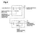
- the reference voltage value V ref output from the reference voltage hold circuit 300 and input to the comparison circuit A 402 defines the maximum value of the difference signal voltages V n3 that can be A/D-converted by the A/D conversion circuit 400 without causing any saturation, i.e., the A/D conversion range.
- the entire A/D conversion range can be effectively utilized. That is, the solid-state imaging device according to this embodiment is not saturated even when the incident light intensity is high and obtains an excellent resolution for A/D conversion even when the incident light intensity is low.
- This imaging device is mounted on a circuit board CB. That is, a socket SKT is fixed on the circuit board CB, and the imaging device is fitted into the socket SKT such that the terminals TM come into contact with the inner surface of the socket SKT.
- a light source LED is also arranged on the circuit board CB. That is, this device has the light source LED which supplies light to be incident on the solid-state image sensing element SC, and the solid-state imaging device SC and light source LED are fixed on the single circuit board CB.
- the principle of triangulation can be used. That is, since the incident position of the light spot changes depending on the distance between the light source LED and the semiconductor chip SC, this device can be used for a distance measuring device.
- This arithmetic processing is executed by a digital processor mounted on the circuit board CB.
- the present invention can be used for a solid-state imaging device and distance measuring device.
Landscapes
- Engineering & Computer Science (AREA)
- Theoretical Computer Science (AREA)
- Multimedia (AREA)
- Signal Processing (AREA)
- Transforming Light Signals Into Electric Signals (AREA)
- Automatic Focus Adjustment (AREA)
- Length Measuring Devices By Optical Means (AREA)
- Measurement Of Optical Distance (AREA)
- Analogue/Digital Conversion (AREA)
Applications Claiming Priority (3)
| Application Number | Priority Date | Filing Date | Title |
|---|---|---|---|
| JP22247599 | 1999-08-05 | ||
| JP22247599 | 1999-08-05 | ||
| PCT/JP2000/005284 WO2001011870A1 (fr) | 1999-08-05 | 2000-08-07 | Dispositif d'imagerie a semi-conducteur et dispositif de telemetrie |
Publications (3)
| Publication Number | Publication Date |
|---|---|
| EP1206131A1 true EP1206131A1 (fr) | 2002-05-15 |
| EP1206131A4 EP1206131A4 (fr) | 2004-04-21 |
| EP1206131B1 EP1206131B1 (fr) | 2005-12-07 |
Family
ID=16783010
Family Applications (1)
| Application Number | Title | Priority Date | Filing Date |
|---|---|---|---|
| EP00950024A Expired - Lifetime EP1206131B1 (fr) | 1999-08-05 | 2000-08-07 | Dispositif d'imagerie a semi-conducteur et dispositif de telemetrie |
Country Status (6)
| Country | Link |
|---|---|
| US (1) | US6956607B2 (fr) |
| EP (1) | EP1206131B1 (fr) |
| JP (1) | JP4463457B2 (fr) |
| AU (1) | AU6320300A (fr) |
| DE (1) | DE60024641T2 (fr) |
| WO (1) | WO2001011870A1 (fr) |
Cited By (3)
| Publication number | Priority date | Publication date | Assignee | Title |
|---|---|---|---|---|
| US6642501B2 (en) * | 1999-07-16 | 2003-11-04 | Hamamatsu Photonics K.K. | Photo-detecting apparatus |
| EP1081941A3 (fr) * | 1999-08-31 | 2004-01-07 | Taiwan Advanced Sensors Corporation | Circuit à double échantillonnage correlé avec autocompensation |
| EP1575282A4 (fr) * | 2002-12-16 | 2009-03-04 | Hamamatsu Photonics Kk | Capteur optique |
Families Citing this family (22)
| Publication number | Priority date | Publication date | Assignee | Title |
|---|---|---|---|---|
| EP1314969B1 (fr) * | 2000-08-03 | 2006-03-22 | Hamamatsu Photonics K. K. | Detecteur optique |
| US6947607B2 (en) | 2002-01-04 | 2005-09-20 | Warner Bros. Entertainment Inc. | Reduction of differential resolution of separations |
| US7127125B2 (en) * | 2002-01-04 | 2006-10-24 | Warner Bros. Entertainment Inc. | Registration of separations |
| US7092584B2 (en) * | 2002-01-04 | 2006-08-15 | Time Warner Entertainment Company Lp | Registration of separations |
| JP4293588B2 (ja) | 2002-12-16 | 2009-07-08 | 浜松ホトニクス株式会社 | 光検出装置 |
| US7414653B2 (en) * | 2003-12-19 | 2008-08-19 | Micron Technology, Inc. | Dark reduction via feedback control of photodiode bias |
| US7446806B2 (en) * | 2003-12-19 | 2008-11-04 | Symbol Technologies, Inc. | Single chip, noise-resistant, one-dimensional, CMOS sensor for target imaging |
| JP2005218052A (ja) * | 2004-02-02 | 2005-08-11 | Hamamatsu Photonics Kk | 光検出装置 |
| JP4429796B2 (ja) | 2004-05-10 | 2010-03-10 | 浜松ホトニクス株式会社 | センサ装置 |
| JP4314172B2 (ja) * | 2004-08-30 | 2009-08-12 | シャープ株式会社 | 増幅型固体撮像装置 |
| KR100674957B1 (ko) * | 2005-02-23 | 2007-01-26 | 삼성전자주식회사 | 임의의 서브-샘플링 레이트로 아날로그 신호를 평균화하여서브-샘플링하는 고체 촬상 소자 및 그 구동 방법 |
| TWI349489B (en) * | 2006-09-07 | 2011-09-21 | Realtek Semiconductor Corp | Image processing device and method |
| EP2232197A4 (fr) * | 2007-11-07 | 2014-04-02 | Tomra Systems Asa | Appareil, unité optique et dispositifs utilisables pour la détection d'objets |
| US7732749B2 (en) * | 2008-02-28 | 2010-06-08 | Respiratory Management Technology | System and method for measuring the output of a photodetector and for reducing sensitivity to temperature variations |
| JP5616025B2 (ja) * | 2009-01-22 | 2014-10-29 | 株式会社トプコン | 光波距離測定方法及び光波距離測定装置 |
| JP4837757B2 (ja) | 2009-03-16 | 2011-12-14 | シャープ株式会社 | 光学式測距センサおよび電子機器 |
| JP5218513B2 (ja) * | 2010-09-30 | 2013-06-26 | オムロン株式会社 | 変位センサ |
| JP5858652B2 (ja) * | 2011-06-08 | 2016-02-10 | キヤノン株式会社 | 固体撮像装置及び固体撮像装置の駆動方法 |
| US9241128B2 (en) | 2013-02-14 | 2016-01-19 | Warner Bros. Entertainment Inc. | Video conversion technology |
| CN115468841A (zh) * | 2014-07-28 | 2022-12-13 | 伊利诺斯工具制品有限公司 | 实时视频引伸计 |
| JP2021044638A (ja) * | 2019-09-09 | 2021-03-18 | 株式会社東芝 | 電子回路 |
| CN113126067A (zh) * | 2019-12-26 | 2021-07-16 | 华为技术有限公司 | 激光安全电路及激光安全设备 |
Family Cites Families (20)
| Publication number | Priority date | Publication date | Assignee | Title |
|---|---|---|---|---|
| JPS5214112B2 (fr) * | 1973-02-22 | 1977-04-19 | ||
| JPS61144175A (ja) * | 1984-12-17 | 1986-07-01 | Matsushita Electric Ind Co Ltd | キズ補正装置 |
| KR900000332B1 (ko) * | 1984-06-01 | 1990-01-25 | 마쯔시다덴기산교 가부시기갸이샤 | 흠 보정장치 |
| JPH01222583A (ja) * | 1988-03-02 | 1989-09-05 | Canon Inc | 光電変換装置並びに該装置の蓄積動作を制御する蓄積制御装置 |
| US5343201A (en) * | 1988-04-07 | 1994-08-30 | Canon Kabushiki Kaisha | A-D converter |
| JP2667871B2 (ja) * | 1988-04-19 | 1997-10-27 | キヤノン株式会社 | A−d変換器 |
| JPH053554A (ja) * | 1991-02-28 | 1993-01-08 | Kyocera Corp | 固体撮像装置 |
| JPH04322575A (ja) * | 1991-04-23 | 1992-11-12 | Mitsubishi Electric Corp | アナログ/ディジタル変換方式 |
| FR2685846B1 (fr) * | 1991-12-31 | 1995-10-06 | Thomson Csf | Camera a detecteur, munie d'une protection electronique. |
| JP2738899B2 (ja) * | 1993-03-19 | 1998-04-08 | 浜松ホトニクス株式会社 | 固体撮像装置 |
| JPH0767152B2 (ja) * | 1993-03-25 | 1995-07-19 | 日本電気株式会社 | イメージセンサとその駆動方法 |
| JPH0772256A (ja) * | 1993-09-01 | 1995-03-17 | Fuji Photo Film Co Ltd | 画像信号補正装置および方法 |
| JPH08149376A (ja) * | 1994-11-18 | 1996-06-07 | Olympus Optical Co Ltd | 固体撮像装置 |
| JP3817294B2 (ja) * | 1996-04-01 | 2006-09-06 | 浜松ホトニクス株式会社 | 固体撮像装置 |
| US5831258A (en) * | 1996-08-20 | 1998-11-03 | Xerox Corporation | Pixel circuit with integrated amplifer |
| JP3000959B2 (ja) * | 1997-05-20 | 2000-01-17 | 日本電気株式会社 | 積層型固体撮像素子 |
| WO2000045592A1 (fr) * | 1999-01-29 | 2000-08-03 | Hamamatsu Photonics K.K. | Dispositif photodetecteur |
| JP4358351B2 (ja) * | 1999-04-27 | 2009-11-04 | 浜松ホトニクス株式会社 | 光検出装置 |
| JP2000346643A (ja) * | 1999-06-09 | 2000-12-15 | Hamamatsu Photonics Kk | 光位置検出装置および距離センサ |
| JP4119052B2 (ja) * | 1999-07-16 | 2008-07-16 | 浜松ホトニクス株式会社 | 光検出装置 |
-
2000
- 2000-08-07 EP EP00950024A patent/EP1206131B1/fr not_active Expired - Lifetime
- 2000-08-07 WO PCT/JP2000/005284 patent/WO2001011870A1/fr not_active Ceased
- 2000-08-07 AU AU63203/00A patent/AU6320300A/en not_active Abandoned
- 2000-08-07 DE DE60024641T patent/DE60024641T2/de not_active Expired - Lifetime
- 2000-08-07 JP JP2001515619A patent/JP4463457B2/ja not_active Expired - Fee Related
-
2002
- 2002-02-01 US US10/060,167 patent/US6956607B2/en not_active Expired - Fee Related
Cited By (4)
| Publication number | Priority date | Publication date | Assignee | Title |
|---|---|---|---|---|
| US6642501B2 (en) * | 1999-07-16 | 2003-11-04 | Hamamatsu Photonics K.K. | Photo-detecting apparatus |
| EP1081941A3 (fr) * | 1999-08-31 | 2004-01-07 | Taiwan Advanced Sensors Corporation | Circuit à double échantillonnage correlé avec autocompensation |
| EP1575282A4 (fr) * | 2002-12-16 | 2009-03-04 | Hamamatsu Photonics Kk | Capteur optique |
| US7612814B2 (en) | 2002-12-16 | 2009-11-03 | Hamamatsu Photonics K.K. | Optical sensor |
Also Published As
| Publication number | Publication date |
|---|---|
| US20020085104A1 (en) | 2002-07-04 |
| DE60024641D1 (de) | 2006-01-12 |
| EP1206131B1 (fr) | 2005-12-07 |
| AU6320300A (en) | 2001-03-05 |
| EP1206131A4 (fr) | 2004-04-21 |
| WO2001011870A1 (fr) | 2001-02-15 |
| US6956607B2 (en) | 2005-10-18 |
| DE60024641T2 (de) | 2006-08-17 |
| JP4463457B2 (ja) | 2010-05-19 |
Similar Documents
| Publication | Publication Date | Title |
|---|---|---|
| EP1206131B1 (fr) | Dispositif d'imagerie a semi-conducteur et dispositif de telemetrie | |
| US6606123B2 (en) | Photosensitive device | |
| JP4119052B2 (ja) | 光検出装置 | |
| KR100717665B1 (ko) | 시적분 픽셀 센서에서의 디지털 이중 샘플링 | |
| CN106664379B (zh) | 高动态范围像素和用于操作高动态范围像素的方法 | |
| EP1052846A2 (fr) | Capteur d'images corporant mesure du temps de saturation pour l'augmentation de la gamme dynamique | |
| US6246436B1 (en) | Adjustable gain active pixel sensor | |
| US20140078360A1 (en) | Imagers with improved analog-to-digital converters | |
| JP2000162041A (ja) | 光検出装置 | |
| JP4358351B2 (ja) | 光検出装置 | |
| JPWO2001011870A1 (ja) | 固体撮像装置及び測距装置 | |
| JP7165873B2 (ja) | 撮像処理回路、撮像システム、撮像処理方法及びプログラム | |
| US5027148A (en) | Autofocus chip with reference level determination circuit | |
| US20020113887A1 (en) | CMOS image sensor with extended dynamic range | |
| EP1416424B1 (fr) | Réseau de photodétecteurs avec une comparaison de signal au niveau du pixel | |
| JP2004264034A (ja) | 光検出装置 | |
| CN109643523B (zh) | 像素电路以及图像传感系统 | |
| CN101023330A (zh) | 光检测装置 | |
| JP2719086B2 (ja) | 光検出装置 | |
| JP2005121398A (ja) | 光検出装置及びそれを用いた測距装置 | |
| Kim et al. | An image sensor with in-pixel selective-charge-subtraction circuits for selective light detection | |
| JPH05312645A (ja) | 光センサ回路 | |
| JPH05244487A (ja) | 光センサアレイの信号変換装置 | |
| JP2004072542A (ja) | 光センサ | |
| Pain | Linear dynamic range enhancement in a CMOS imager |
Legal Events
| Date | Code | Title | Description |
|---|---|---|---|
| PUAI | Public reference made under article 153(3) epc to a published international application that has entered the european phase |
Free format text: ORIGINAL CODE: 0009012 |
|
| 17P | Request for examination filed |
Effective date: 20020226 |
|
| AK | Designated contracting states |
Kind code of ref document: A1 Designated state(s): AT BE CH CY DE DK ES FI FR GB GR IE IT LI LU MC NL PT SE |
|
| AX | Request for extension of the european patent |
Free format text: AL;LT;LV;MK;RO;SI |
|
| A4 | Supplementary search report drawn up and despatched |
Effective date: 20040304 |
|
| RIC1 | Information provided on ipc code assigned before grant |
Ipc: 7H 03M 1/18 B Ipc: 7H 04N 5/335 A Ipc: 7G 01C 3/10 B Ipc: 7G 02B 7/32 B Ipc: 7G 01C 3/06 B Ipc: 7G 01B 1/00 B Ipc: 7G 06K 9/46 B |
|
| RBV | Designated contracting states (corrected) |
Designated state(s): DE FR GB IT |
|
| 17Q | First examination report despatched |
Effective date: 20040621 |
|
| GRAP | Despatch of communication of intention to grant a patent |
Free format text: ORIGINAL CODE: EPIDOSNIGR1 |
|
| GRAS | Grant fee paid |
Free format text: ORIGINAL CODE: EPIDOSNIGR3 |
|
| GRAA | (expected) grant |
Free format text: ORIGINAL CODE: 0009210 |
|
| AK | Designated contracting states |
Kind code of ref document: B1 Designated state(s): DE FR GB IT |
|
| REG | Reference to a national code |
Ref country code: GB Ref legal event code: FG4D |
|
| REF | Corresponds to: |
Ref document number: 60024641 Country of ref document: DE Date of ref document: 20060112 Kind code of ref document: P |
|
| ET | Fr: translation filed | ||
| PLBE | No opposition filed within time limit |
Free format text: ORIGINAL CODE: 0009261 |
|
| STAA | Information on the status of an ep patent application or granted ep patent |
Free format text: STATUS: NO OPPOSITION FILED WITHIN TIME LIMIT |
|
| 26N | No opposition filed |
Effective date: 20060908 |
|
| PGFP | Annual fee paid to national office [announced via postgrant information from national office to epo] |
Ref country code: GB Payment date: 20120801 Year of fee payment: 13 |
|
| PGFP | Annual fee paid to national office [announced via postgrant information from national office to epo] |
Ref country code: DE Payment date: 20120731 Year of fee payment: 13 Ref country code: FR Payment date: 20120823 Year of fee payment: 13 Ref country code: IT Payment date: 20120811 Year of fee payment: 13 |
|
| GBPC | Gb: european patent ceased through non-payment of renewal fee |
Effective date: 20130807 |
|
| PG25 | Lapsed in a contracting state [announced via postgrant information from national office to epo] |
Ref country code: DE Free format text: LAPSE BECAUSE OF NON-PAYMENT OF DUE FEES Effective date: 20140301 |
|
| REG | Reference to a national code |
Ref country code: FR Ref legal event code: ST Effective date: 20140430 |
|
| REG | Reference to a national code |
Ref country code: DE Ref legal event code: R119 Ref document number: 60024641 Country of ref document: DE Effective date: 20140301 |
|
| PG25 | Lapsed in a contracting state [announced via postgrant information from national office to epo] |
Ref country code: IT Free format text: LAPSE BECAUSE OF NON-PAYMENT OF DUE FEES Effective date: 20130807 |
|
| PG25 | Lapsed in a contracting state [announced via postgrant information from national office to epo] |
Ref country code: GB Free format text: LAPSE BECAUSE OF NON-PAYMENT OF DUE FEES Effective date: 20130807 |
|
| PG25 | Lapsed in a contracting state [announced via postgrant information from national office to epo] |
Ref country code: FR Free format text: LAPSE BECAUSE OF NON-PAYMENT OF DUE FEES Effective date: 20130902 |