EP1207409A1 - Polarisations- und wellenlängenunabhängiger optischer Leistungsteilerschaltkreis - Google Patents
Polarisations- und wellenlängenunabhängiger optischer Leistungsteilerschaltkreis Download PDFInfo
- Publication number
- EP1207409A1 EP1207409A1 EP02075243A EP02075243A EP1207409A1 EP 1207409 A1 EP1207409 A1 EP 1207409A1 EP 02075243 A EP02075243 A EP 02075243A EP 02075243 A EP02075243 A EP 02075243A EP 1207409 A1 EP1207409 A1 EP 1207409A1
- Authority
- EP
- European Patent Office
- Prior art keywords
- wave guiding
- section
- modal
- mode
- waveguide
- Prior art date
- Legal status (The legal status is an assumption and is not a legal conclusion. Google has not performed a legal analysis and makes no representation as to the accuracy of the status listed.)
- Withdrawn
Links
Images


Classifications
-
- G—PHYSICS
- G02—OPTICS
- G02B—OPTICAL ELEMENTS, SYSTEMS OR APPARATUS
- G02B6/00—Light guides; Structural details of arrangements comprising light guides and other optical elements, e.g. couplings
- G02B6/10—Light guides; Structural details of arrangements comprising light guides and other optical elements, e.g. couplings of the optical waveguide type
- G02B6/12—Light guides; Structural details of arrangements comprising light guides and other optical elements, e.g. couplings of the optical waveguide type of the integrated circuit kind
- G02B6/122—Basic optical elements, e.g. light-guiding paths
- G02B6/125—Bends, branchings or intersections
-
- G—PHYSICS
- G02—OPTICS
- G02B—OPTICAL ELEMENTS, SYSTEMS OR APPARATUS
- G02B6/00—Light guides; Structural details of arrangements comprising light guides and other optical elements, e.g. couplings
- G02B6/10—Light guides; Structural details of arrangements comprising light guides and other optical elements, e.g. couplings of the optical waveguide type
- G02B6/14—Mode converters
-
- G—PHYSICS
- G02—OPTICS
- G02B—OPTICAL ELEMENTS, SYSTEMS OR APPARATUS
- G02B6/00—Light guides; Structural details of arrangements comprising light guides and other optical elements, e.g. couplings
- G02B6/10—Light guides; Structural details of arrangements comprising light guides and other optical elements, e.g. couplings of the optical waveguide type
- G02B6/12—Light guides; Structural details of arrangements comprising light guides and other optical elements, e.g. couplings of the optical waveguide type of the integrated circuit kind
- G02B2006/12083—Constructional arrangements
- G02B2006/12097—Ridge, rib or the like
-
- G—PHYSICS
- G02—OPTICS
- G02B—OPTICAL ELEMENTS, SYSTEMS OR APPARATUS
- G02B6/00—Light guides; Structural details of arrangements comprising light guides and other optical elements, e.g. couplings
- G02B6/10—Light guides; Structural details of arrangements comprising light guides and other optical elements, e.g. couplings of the optical waveguide type
- G02B6/12—Light guides; Structural details of arrangements comprising light guides and other optical elements, e.g. couplings of the optical waveguide type of the integrated circuit kind
- G02B2006/12133—Functions
- G02B2006/1215—Splitter
Definitions
- the invention is in the field of integrated optical circuits. More particularly, it relates to an integrated optical waveguide circuit for splitting an optical input signal into two output signals with optical powers in a predetermined splitting ratio.
- the present application is a division application of the parent application European Patent application No. 95201401.7.
- Splitting optical signals is one of the most important functions in an optical system.
- optical 1 ⁇ N splitters are known, which often are composed of optical 3dB splitters.
- a 3dB splitter is a power splitter in which the optical power of an optical input signal is evenly distributed over two output signals, having therefore a splitting ratio of 50/50.
- For optical signal monitoring or in optical control loops often smaller fractions, for example 10 %, are split out of the optical power of an optical signal.
- known splitters can roughly be distinguished into two kinds.
- a first kind is based on interference.
- Splitting circuits in which a direction coupling device or an MZ-interferometer is applied belong to this kind.
- a second splitter kind is based on symmetry.
- the type most generally known of this kind is the symmetric Y splitter which possesses a mono-modal wave guiding trunk, branching symmetrically into two mono-modal wave guiding branches. Due to its symmetry, it principally is a 3dB splitter.
- a second type of said second kind, for example, is known through references [1] and [2].
- Said second type relates to an asymmetric Y splitter having a mono-modal trunk, which widens adiabatically to a bi- or multi-modal waveguide and subsequently splits into two mono-modal branches having different propagation constants at a relatively large splitting angle.
- the coupling area adjacent to the splitting point between the two branches forms a disruption, as a result of which partial conversions in propagation modes are caused, in an optical signal entering via the trunk, from the zero order to the first order.
- the signals which have different order of propagation mode subsequently further propagate via the different branches.
- the extent of conversion consequently determines the splitting ratio and, inter alia, depends on the widths chosen for the two branches and on the size of the angle between both branches.
- a splitting point which to a large degree reflection-free is attained by having the effective refraction index in the propagation direction decrease gradually in the area between both branches starting from the splitting point.
- this known asymmetric Y splitter is polarisation-independent to a high degree and to some extent wavelength-independent, a desired specific splitting ratio cannot be realised easily.
- a third splitter type of the second kind, with which a well-defined fraction can be split out of an optical signal, is known through reference [3]. Said splitter is a combination of a mode converter and an asymmetric Y splitter used as a modus splitter.
- the asymmetric Y splitter has a bi-modal wave guiding trunk which splits at a relatively small angle into two mono-modal branches having different propagation constants and is incorporated in the bi-modal trunk of a mode-converter.
- the light mainly couples in the one or the other of both branches.
- a desired fraction of a zero propagation mode is converted into a first propagation mode.
- said known splitter has a splitting ratio which can be defined well, as a consequence of the interferometric nature of the mode converter it is selective, to a high extent, for wavelength and polarisation of the optical signal used.
- Reference [4] discloses a further example of power splitting devices of the first kind.
- This known device is based on a mono-modal input waveguide provided with an abrupt bend followed on a critical distance by a symmetrical branch.
- the bend functions as a mode converter for partially converting a guided mode signal of the input waveguide into radiation mode signals, part of which is picked up by a widening waveguiding portion of the symmetrical branch and reconverted to local guided modes.
- the symmetrical branch is dimensioned as a 50/50 power splitter, in which non-converted and reconverted guided mode signal parts are split up, in such a way that the split portions in each of the two mono-modal wave guiding arms of the Y-branch will interfere, resulting in a final power splitting ratio which depends on the amplitudes of and the phase differences between the interfering portions.
- the amplitudes and phase differences appear to depend strongly on the critical bend-to-branch distance.
- This known device has likewise the disadvantages of the first kind already mentioned above.
- the above-mentioned parent application describes a power splitter which can be integrated, in a simple manner, with a well-definable splitting ratio, which power splitter is based on a combination of a mode splitter with a mode converter not based upon interference.
- the described splitter is based on the fact that a discontinuity in a bimodal or, more in general, a multi-modal waveguide causes a partial mode conversion in an optical signal, propagating in accordance with a first propagation mode in said waveguide, to a signal propagating in a second propagation mode, with the two propagation modes differing in order number.
- the width(s) of the wave guiding sections at both sides of the discontinuity in the bi- or multi-modal waveguide can be chosen in such manner that a high extent of polarisation-independence is also obtained.
- This means that such a discontinuity which can be dimensioned to a desired conversion fraction in a simple manner can very well be used as an interference-free mode converter.
- the splitting device of the parent application is based on such a discontinuity. Further measures are described for avoiding, or at least substantially suppressing, reflections which generally occur at a discontinuity in a waveguide.
- a discontinuity may define a coupling area in which the conversion or coupling takes place between guided modes of different order number, it appeared that the length of the coupling area can be designed in such a manner that such reflections are largely suppressed and yet the desired conversion fraction is obtained.
- An object of the invention is to provide a power splitter of similar kind as described in the parent application, the measures to be taken being not so much directed to suppressing reflections, as directed to limit the total length of the integrated circuit of the power splitter, while retaining a high degree of freedom for the choice of the waveguide profiles of the wave guiding sections on either side of the discontinuity.
- An integrated optical waveguide circuit for splitting an optical input signal into two output signals having optical powers in a predetermined splitting ratio comprising an input waveguide and first and second output waveguides, a mode converter including an input wave guiding section coupled to the input waveguide, and an output wave guiding section, and a mode splitter including an asymmetric Y-junction which is provided with a wave guiding trunk coupled to the output wave guiding section of the mode converter, and with first and second wave guiding branches, respectively coupled to said first and second output waveguides, the mode converter converting an optical input signal of a first guided mode into an output signal including a non-converted part of the input signal propagating in the first guided mode and a converted part, which is a fraction of the input signal, propagating in a second guided mode in order different from the first guided mode, and the mode splitter emitting signals which enter via the wave guiding trunk and propagate in propagation modes of different order, via different wave guiding branches, which optical circuit is of a kind known from reference [3], is according to the invention
- the adiabatic taper sections may adjoin each other in the discontinuity either in a symmetric or in a asymmetric manner.
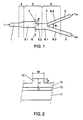
- FIG. 1 shows diagrammatically an optical power splitting circuit to which the invention can be applied.
- the circuit comprises a mono-modal wave guiding input channel 1 and two mono-modal wave guiding output channels 2 and 3. Between the input channel 1 and the two output channels 2 and 3 have been incorporated, successively, a taper section 4 for the adiabatic transition from a mono-modal to a bi-modal wave guiding channel, a bi-modal wave guiding intermediate section 5 directly adjoining the taper section 4, and an asymmetric Y splitter 6 dimensioned as a mode splitter and having a bi-modal wave guiding trunk 6.1 and two mono-modal wave guiding branches 6.2 and 6.3 differing in propagation constants.
- the wave guiding branches 6.2 and 6.3 mutually divert at a diversion angle ⁇ , and outside their mutual interaction area pass into the output channels 2 and 3, respectively.
- the bi-modal intermediary section 5 comprises two subsections 5.1 and 5.2, which adjoin each other via a discontinuity 7, i.e. are coupled to each other.
- the plane in which the two sections are coupled to each other is called coupling plane, indicated by K in the Figure. If, in the coupling plane, the cross section profiles of the two wave guiding subsections 5.1 and 5.2 do not exactly fall over each other, this is a jumpy discontinuity.
- the extent to which the cross section profiles of the two wave guiding subsections 5.1 and 5.2 divert from each other in the coupling plane K determines the extent of the discontinuity.
- the discontinuity is symbolically represented by a mutual offset of the two subsections over a distance indicated by x.
- a discontinuity in a waveguide therefore has the meaning of such an abrupt transition between two successive subsections of the waveguide, that such conversions can take place between guided modes having different order numbers.
- a discontinuity is symmetric if the two successive subsections of the waveguide and the intermediately located transition have a common plane of symmetry. Any other discontinuity is asymmetric.
- the extent of conversion i.e. the size of the coupling constant, has been found to depend, to a large degree, on the extent of discontinuity. This will hereinafter be illustrated on the basis of a discontinuity in a channel-like type of waveguide generally used in integrated optical devices on the basis of semiconducting materials, i.e. a rib type waveguide. Of such a type of waveguide, in FIG.
- a cross section is shown, only by way of example on the basis of indium phosphide (InP).
- InP indium phosphide
- a light-guiding layer 13 is located, the so-called quaternary layer of InGaAsP having a thickness t.
- the top layer 12 locally shows, over the length of the guide, a rib-like elevation 12.1 having a height h and width w, which for example, is obtained by partially etching away a top layer which initially had a thickness H.
- FIG. 3 shows a first asymmetric discontinuity to which two wave guiding sections a and b, respectively adjoin each other laterally in an offset manner, having central axes h a and h b and having one and the same waveguide profile, i.c. an identical width.
- the central axes are offset over a distance x.
- the circuit When using such an asymmetric discontinuity in the optical circuit of FIG. 1, the circuit operates as follows.
- An optical signal I i entering the mono-modal input channel 1 propagates in the fundamental mode, i.e. zero order mode, via the taper section 4 and the bi-modal subsection 5.1 of the section 5 as far as the asymmetric discontinuity 7.
- the coupling plane K of the discontinuity 7 a fraction ⁇ of the signal I i is converted into a signal which further propagates in the first order guided mode in the bi-modal subsection 5.2, whereas a non-converted part ⁇ of the signal I i further propagates in the zero order guided mode.
- ⁇ and ⁇ are ratio numbers of signal intensities.
- the parts propagate in the asymmetric Y splitter 6 along different wave guiding branches 6.2 and 6.3 to the output channels 2 and 3.
- the branch 6.2 has the lowest propagation constant (which in case of the waveguide profile of FIG. 2 corresponds to the smallest width)
- a signal I o1 emitting out of output channel 2 corresponds to the converted fraction ⁇ of the input signal I i
- a signal I o2 emitting out of output channel 3 corresponds to the non-converted part ⁇ .
- Asymmetric Y splitter 6 Asymmetric Y splitter 6:
- the subsection 5.2 of the intermediate section 5 and the trunk 6.1 of the asymmetric Y splitter 6 are in this connection simulated as being one adiabatic taper having a length of 90 ⁇ m and a width decreasing from 6.0 ⁇ m to 5.2 ⁇ m.
- FIG. 4A shows that, by selecting the appropriate x, any value for the splitting ratio ⁇ / ⁇ between 0 and 1 can be realised; whereas FIG. 4B shows that, in this connection, the attenuation D remains restricted to approximately half of the signal intensity (approx. -3dB).
- the fraction ⁇ is proportional to the square of x.
- the refraction indexes are, respectively, 3.209 and 3.169 in InP, and 3.352 and 3.289 in InGaAsP.
- the following splitting ratios (in dB) were found: (TM, 1.55) 10dB (TE, 1.55) 10.7dB (TM, 1.3) 9.8dB (TE, 1.3) 9.9dB
- the widths of the wave guiding subsections 5.1 and 5.2 are maximally chosen for a bi-modal propagation for both polarisations TE and TM.
- the input channel 1 has been realised as a bi-modal waveguide, which without a taper section passes directly into the subsection 5.1 of the intermediate section 5, of a first order mode input signal a fraction which is dependent on x is converted into a zero order mode signal by the discontinuity 7, which signal then propagates further in the Y splitter via a branch other than the non-converted part.
- a circuit thus realised a fraction determined by the size of x can be split from a first order signal.
- the coupling plane K of the discontinuity is chosen perpendicular to the direction of the central axes h a and h b . This is not necessary.
- an angle ⁇ 90° between the central axes and the coupling plane the reflecting action of the discontinuity is also decreased.
- a first modification of such a discontinuity is represented in FIG. 5A.
- the angle ⁇ is chosen in such manner that edge points 51, 52, 53 and 54 of a rib pattern, realising the wave guiding sections a and b and which edge points being situated in the coupling plane, correspond to obtuse angles. Obtuse-angled edges can more precisely be defined in a photo-lithographic manner.
- the discontinuity extends in the propagation direction over a length y equal to the length of the projection of the coupling plane K between the edge points 51 and 54 on one of the central axes h a or h b . In fact, this is no longer a coupling plane but a coupling area KG.
- FIG. 5B a second modification of a discontinuity having a decreased reflecting action is shown.
- the discontinuity is formed by a short taper 55 having length y between two mutual offset wave guiding sections a and b.
- the length y must be much smaller than the beat length between the guided modes of the non-converted signal part and the converted signal part in the wave guiding section b, consequently beyond the discontinuity.
- N.B. beat length must be understood as the propagation distance over which the phase-relations between two guided modes repeat themselves).
- the length y must be much larger than the beat length between the guided modes of the input signal and a signal reflected at the discontinuity in the wave guiding section a.
- the beat length ⁇ 0 ⁇ 0 is in the order of 1 ⁇ m
- the beat length ⁇ 0 ⁇ 1 is in the order of 100 ⁇ m and higher.
- a good choice for the length y therefore is approx. 10 ⁇ m.
- Such a choice accordingly means that the transition between the two wave guiding sections a and b (or the subsections 5.1 and 5.2 in FIG. 1) can be designed such that it functions as a discontinuity for forwards propagating guided modes, but as an adiabatic transition for two guided modes propagating mutually in opposite direction, so that at the transition no or hardly no reflection occurs.
- the length of the wave guiding sections a and b before and after the transition is of no importance. If such a discontinuity is incorporated into the intermediary wave guiding section 5 of the circuit of FIG. 1, in which the length of the subsections 5.1 and 5.2 is in fact chosen as equal to zero, then, according to the invention, a third modification arises as a result of which the total length of the circuit can be restricted.
- the coupling plane K of the discontinuity then is situated directly to the end of the taper section 4.
- the length of the trunk 6.1 of the asymmetric Y splitter can be chosen in such a short manner that a splitting point 8 (this being the point where both branches 6.2 and 6.3 start to divert) is almost situated in the coupling plane K.
- the trunk 6.1 can, according to the invention, also be realised as an adiabatic taper in order to be able to choose, with a given width of the trunk 6.1, at the height of the splitting point 8, the desired width in the coupling plane K.
- FIG. 6A shows a symmetric discontinuity, to which two wave guiding sections c and d adjoin with a common central axis h.
- Said symmetric discontinuity is formed by a jumpy symmetric change in width, i.e. a widening or narrowing in each of both directions perpendicular to the central axis h of in total 2x s .
- FIG. 6A shows, by way of example, a widening. At the location of the widening, a coupling plane K is again formed which is situated perpendicular to the common central axis h.
- FIG. 6B shows a modification of a symmetric discontinuity having a decreased reflecting effect, in which the transition between both wave guiding subsections c and d is formed by a short symmetric taper 61 having a length y s , of which the width increases symmetrically by in total 2x s .
- a coupling area KG exists, having a length y s .
- similar limits apply as expressed in inequality ⁇ 1 ⁇ . If for example the wave guiding sections c and d must both be tri-modal, in the inequality ⁇ 1 ⁇ the propagation constant ⁇ 1 must be replaced by a propagation constant ⁇ 2 for a second order guided mode.
- FIG. 7 diagrammatically shows an exemplary embodiment of an optical power splitting circuit according to the invention, in which a symmetric discontinuity is used.
- the circuit comprises a mono-modal wave guiding input channel 71 and two mono-modal wave guiding output channels 72 and 73. Between the input channel 71 and the two output channels 72 and 73 have been incorporated, successively, an intermediate section 74, and an asymmetric Y splitter 75 dimensioned as a mode splitter and having two wave guiding branches 76 and 77 differing in propagation constants.
- the branch 76 is mono-modal and outside the interaction area with the branch 77 directly passes into the mono-modal output channel 72.
- the wave guiding branch 77 is bi-modal and outside the interaction area with the branch 76 directly passes into the mono-modal output channel 73 via an adiabatic taper 78.
- the intermediate section 74 comprises two adiabatic tapers 79 and 80, which mutually adjoin in a coupling plane K via a symmetric jumpy widening with the size of 2x s .
- the adiabatic taper 79 increases in width from a width which suits a mono-modal waveguide to a waveguide having a desired width, whereas the width of the taper 80 from the coupling plane gradually changes into (in FIG. 7 decreases to) the sum of the widths of the branches 76 and 77 at the height of a splitting point 81, i.e. at the point where the branches 76 and 77 divert.
- the circuit in accordance with FIG. 7 operates in a similar manner as the circuit of FIG. 1.
- a signal I i entering via the input channel 71, propagating in the zero order guided mode reaches the coupling plane K in the transition of the tapers 79 and 80 in the intermediate section 74 in an undisturbed manner.
- There a fraction dependent on the size of x s of the zero order mode signal is converted into a signal which in taper 80 propagates further in a second order guided mode.
- the non-converted part further propagates in the zero order guided mode.
- Arriving at the splitting point 81, the converted part of the signal in the second order mode propagates further as a zero order mode signal in the branch having the lowest propagation constant, i.e.
- the non-converted part of the signal in the zero order mode further propagates via the bi-modal branch 77 and the taper 78, and emits as an output signal I o2 via the output channel 73.
- the splitting behaviour of the exemplary embodiment has also been simulated with the following dimensioning (with the other parameters being the same as used in the simulations relating to the embodiment of FIG. 1): Input channel 71 width 3 ⁇ m Intermediary section 74 taper 79 rib width increasing from 3 ⁇ m to 7.4 ⁇ m over a length of 125 ⁇ m; jumpy widening 2x s 4.6 ⁇ m; taper 80 rib width decreasing from 12.0 ⁇ m to 9.7 ⁇ m over a length of 70 ⁇ m; Asymmetric Y splitter 75 length: approx.
- the attenuation is less than 0.2dB.
- This exemplary embodiment shows an even better polarisation and wavelength-independence.
- the asymmetric Y junction appears to become somewhat longer than in the circuit of FIG. 1.
- the difference in propagation constants between the zero and the second order guided modes is larger than the difference between the zero order and first order guided modes, it may nevertheless be expected that a mode splitter will be more efficient for the first-mentioned pair of modes and can therefore be realised in a shorter manner.
- the wave guiding intermediate section in which the symmetric discontinuity has been incorporated can be chosen much wider, viz.
Landscapes
- Physics & Mathematics (AREA)
- General Physics & Mathematics (AREA)
- Optics & Photonics (AREA)
- Engineering & Computer Science (AREA)
- Microelectronics & Electronic Packaging (AREA)
- Optical Integrated Circuits (AREA)
- Holo Graphy (AREA)
- Spectrometry And Color Measurement (AREA)
Applications Claiming Priority (3)
| Application Number | Priority Date | Filing Date | Title |
|---|---|---|---|
| NL9400993 | 1994-06-17 | ||
| NL9400993A NL9400993A (nl) | 1994-06-17 | 1994-06-17 | Polarisatie- en golflengte-onafhankelijk optisch vermogen splitsend circuit. |
| EP95201401A EP0687926B1 (de) | 1994-06-17 | 1995-05-30 | Optischer Leistungsteilerschaltkreis unabhängig von der Polarisation und Wellenlänge |
Related Parent Applications (1)
| Application Number | Title | Priority Date | Filing Date |
|---|---|---|---|
| EP95201401.7 Division | 1995-05-30 |
Publications (1)
| Publication Number | Publication Date |
|---|---|
| EP1207409A1 true EP1207409A1 (de) | 2002-05-22 |
Family
ID=19864328
Family Applications (2)
| Application Number | Title | Priority Date | Filing Date |
|---|---|---|---|
| EP02075243A Withdrawn EP1207409A1 (de) | 1994-06-17 | 1995-05-30 | Polarisations- und wellenlängenunabhängiger optischer Leistungsteilerschaltkreis |
| EP95201401A Expired - Lifetime EP0687926B1 (de) | 1994-06-17 | 1995-05-30 | Optischer Leistungsteilerschaltkreis unabhängig von der Polarisation und Wellenlänge |
Family Applications After (1)
| Application Number | Title | Priority Date | Filing Date |
|---|---|---|---|
| EP95201401A Expired - Lifetime EP0687926B1 (de) | 1994-06-17 | 1995-05-30 | Optischer Leistungsteilerschaltkreis unabhängig von der Polarisation und Wellenlänge |
Country Status (9)
| Country | Link |
|---|---|
| US (1) | US5524156A (de) |
| EP (2) | EP1207409A1 (de) |
| JP (1) | JP2717779B2 (de) |
| AT (1) | ATE221671T1 (de) |
| CA (1) | CA2151222C (de) |
| DE (1) | DE69527580T2 (de) |
| FI (3) | FI115415B (de) |
| NL (1) | NL9400993A (de) |
| NO (1) | NO952409L (de) |
Families Citing this family (31)
| Publication number | Priority date | Publication date | Assignee | Title |
|---|---|---|---|---|
| US5623568A (en) * | 1995-09-15 | 1997-04-22 | Lucent Technologies Inc. | Compact and fabrication tolerant high speed digital optical Y-switches |
| US5719976A (en) * | 1995-10-24 | 1998-02-17 | Lucent Technologies, Inc. | Optimized waveguide structure |
| US5745619A (en) * | 1996-06-07 | 1998-04-28 | Lucent Technologies Inc. | Low-loss optical power splitter for high-definition waveguides |
| JP3360547B2 (ja) | 1996-10-24 | 2002-12-24 | 富士ゼロックス株式会社 | 光バスおよび信号処理装置 |
| US6169757B1 (en) * | 1997-09-26 | 2001-01-02 | Scott A. Merritt | Intermodal phase difference controller for beam angle modulation in index guided semiconductor devices |
| WO1999063375A1 (en) * | 1998-06-04 | 1999-12-09 | California Institute Of Technology | Optical devices based on energy transfer between different modes in optical waveguide |
| US6236784B1 (en) * | 1998-08-10 | 2001-05-22 | Hitachi, Ltd. | Y branching optical waveguide and optical integrated circuit |
| US6275627B1 (en) * | 1998-09-25 | 2001-08-14 | Corning Incorporated | Optical fiber having an expanded mode field diameter and method of expanding the mode field diameter of an optical fiber |
| JP3594899B2 (ja) | 2000-12-13 | 2004-12-02 | 株式会社大井製作所 | 車両用サンルーフの制御装置 |
| US20030133663A1 (en) * | 2002-01-16 | 2003-07-17 | Jds Uniphase Corporation | Integrated optical splitter |
| JP3795821B2 (ja) * | 2002-03-29 | 2006-07-12 | 日本発条株式会社 | 光分岐器 |
| US7027673B1 (en) * | 2002-06-19 | 2006-04-11 | Luxtera, Inc. | Integrated dual waveguides |
| US6915047B1 (en) * | 2003-03-24 | 2005-07-05 | Inplane Photonics, Inc. | Broadband, polarization independent integrated optical tap |
| DE102007004891A1 (de) * | 2007-01-31 | 2008-08-14 | CCS Technology, Inc., Wilmington | Optischer Verzweiger |
| JP5222791B2 (ja) * | 2009-06-01 | 2013-06-26 | 富士通株式会社 | 光導波路 |
| CN102879859A (zh) * | 2012-08-20 | 2013-01-16 | 东南大学 | 集成型光分路器 |
| CN103823306A (zh) * | 2012-11-19 | 2014-05-28 | 鸿富锦精密工业(深圳)有限公司 | 光输出装置 |
| US20150104130A1 (en) * | 2013-10-14 | 2015-04-16 | Cisco Technology, Inc. | Optical power splitter |
| CN110455405A (zh) * | 2018-05-08 | 2019-11-15 | 华为技术有限公司 | 光分束器、光功率监测装置及激光器芯片 |
| US11500154B1 (en) * | 2019-10-18 | 2022-11-15 | Apple Inc. | Asymmetric optical power splitting system and method |
| US12372724B2 (en) | 2020-09-23 | 2025-07-29 | Apple Inc. | Light splitting device |
| US11906778B2 (en) | 2020-09-25 | 2024-02-20 | Apple Inc. | Achromatic light splitting device with a high V number and a low V number waveguide |
| JP2023028951A (ja) * | 2021-08-20 | 2023-03-03 | 富士通オプティカルコンポーネンツ株式会社 | タップカプラ、光通信装置及び光分岐方法 |
| US12487407B2 (en) | 2021-09-24 | 2025-12-02 | Apple Inc. | Compact light splitting devices and methods |
| US11971574B2 (en) | 2021-09-24 | 2024-04-30 | Apple Inc. | Multi-mode devices for multiplexing and de-multiplexing |
| EP4273599A1 (de) | 2022-05-05 | 2023-11-08 | Apple Inc. | Kompakter optischer splitter |
| US12510708B2 (en) | 2022-09-02 | 2025-12-30 | Cisco Technology, Inc. | Bilayer silicon nitride polarization mode converter |
| US12287512B2 (en) | 2022-09-02 | 2025-04-29 | Cisco Technology, Inc. | Two layer polarization splitter rotator |
| CN117687144A (zh) * | 2022-09-02 | 2024-03-12 | 华为技术有限公司 | 分光器、分光器芯片、通信设备和光分配网 |
| US12372719B2 (en) | 2022-09-06 | 2025-07-29 | Apple Inc. | Compact optical coupler |
| US20240159963A1 (en) * | 2022-11-11 | 2024-05-16 | Cisco Technology, Inc. | Optical power splitters |
Citations (4)
| Publication number | Priority date | Publication date | Assignee | Title |
|---|---|---|---|---|
| US3920314A (en) * | 1973-06-05 | 1975-11-18 | Agency Ind Science Techn | Mode conversion and mode separation branched dielectric waveguide element for light |
| EP0330457A2 (de) * | 1988-02-26 | 1989-08-30 | Matra Marconi Space UK Limited | Optische Serienfilter |
| EP0513919A1 (de) * | 1991-05-16 | 1992-11-19 | Koninklijke KPN N.V. | Modenwandler |
| EP0562695A1 (de) * | 1992-03-27 | 1993-09-29 | Koninklijke KPN N.V. | Regelbarer Polarisationswandler |
Family Cites Families (5)
| Publication number | Priority date | Publication date | Assignee | Title |
|---|---|---|---|---|
| JPS6217708A (ja) * | 1985-07-16 | 1987-01-26 | Matsushita Electric Ind Co Ltd | モ−ド変換装置 |
| US5134671A (en) | 1990-08-03 | 1992-07-28 | At&T Bell Laboratories | Monolithic integrated optical amplifier and photodetector |
| JPH04104229A (ja) * | 1990-08-24 | 1992-04-06 | Furukawa Electric Co Ltd:The | 光モードスプリッタ |
| FR2668615B1 (fr) * | 1990-10-31 | 1992-12-11 | France Etat | Separateur de polarisations pour lumiere guidee. |
| NL9300204A (nl) * | 1993-02-02 | 1994-09-01 | Nederland Ptt | Geintegreerde optische component voor het manipuleren van de polarisatie van optische signalen. |
-
1994
- 1994-06-17 NL NL9400993A patent/NL9400993A/nl not_active Application Discontinuation
-
1995
- 1995-05-30 AT AT95201401T patent/ATE221671T1/de not_active IP Right Cessation
- 1995-05-30 EP EP02075243A patent/EP1207409A1/de not_active Withdrawn
- 1995-05-30 DE DE69527580T patent/DE69527580T2/de not_active Expired - Fee Related
- 1995-05-30 EP EP95201401A patent/EP0687926B1/de not_active Expired - Lifetime
- 1995-05-31 US US08/456,052 patent/US5524156A/en not_active Expired - Lifetime
- 1995-06-07 CA CA002151222A patent/CA2151222C/en not_active Expired - Fee Related
- 1995-06-16 NO NO952409A patent/NO952409L/no not_active Application Discontinuation
- 1995-06-16 FI FI953008A patent/FI115415B/fi active IP Right Grant
- 1995-06-16 JP JP7183167A patent/JP2717779B2/ja not_active Expired - Fee Related
-
2003
- 2003-06-19 FI FI20030927A patent/FI20030927L/fi not_active Application Discontinuation
-
2004
- 2004-12-28 FI FI20041677A patent/FI117030B/fi active IP Right Grant
Patent Citations (4)
| Publication number | Priority date | Publication date | Assignee | Title |
|---|---|---|---|---|
| US3920314A (en) * | 1973-06-05 | 1975-11-18 | Agency Ind Science Techn | Mode conversion and mode separation branched dielectric waveguide element for light |
| EP0330457A2 (de) * | 1988-02-26 | 1989-08-30 | Matra Marconi Space UK Limited | Optische Serienfilter |
| EP0513919A1 (de) * | 1991-05-16 | 1992-11-19 | Koninklijke KPN N.V. | Modenwandler |
| EP0562695A1 (de) * | 1992-03-27 | 1993-09-29 | Koninklijke KPN N.V. | Regelbarer Polarisationswandler |
Non-Patent Citations (4)
| Title |
|---|
| D.YAP ET.AL.: "Coupling between successive Ti:LiNbO3 waveguide bends and branches", APPLIED OPTICS., vol. 23, no. 17, 1 September 1984 (1984-09-01), NEW YORK US, pages 2991 - 2999, XP002193428 * |
| J.J.G.M.VAN DER TOL ET.AL.: "Mode evolution type polarization splitter on InGaAsP/InP", IEEE PHOTONICS TECHNOLOGY LETTERS, vol. 5, no. 12, December 1993 (1993-12-01), NEW YORK US, pages 1412 - 1414, XP000432987 * |
| R.N.THURSTON ET.AL.: "Analysis of mode separation in multichannel branching waveguides", IEEE JOURNAL OF QUANTUM ELECTRONICS., vol. 23, no. 8, August 1987 (1987-08-01), NEW YORK US, pages 1245 - 1254, XP002193429 * |
| S.SAFAVI-NAEINI ET.AL.: "Design and analysis of novel multimode optical filters in dielectric waveguide", JOURNAL OF LIGHTWAVE TECHNOLOGY., vol. 11, no. 12, December 1993 (1993-12-01), NEW YORK US, pages 1970 - 1977, XP000422656 * |
Also Published As
| Publication number | Publication date |
|---|---|
| JPH085852A (ja) | 1996-01-12 |
| DE69527580D1 (de) | 2002-09-05 |
| NO952409L (no) | 1995-12-18 |
| ATE221671T1 (de) | 2002-08-15 |
| NL9400993A (nl) | 1996-02-01 |
| US5524156A (en) | 1996-06-04 |
| EP0687926A1 (de) | 1995-12-20 |
| FI20030927A7 (fi) | 2003-06-19 |
| FI953008L (fi) | 1995-12-18 |
| CA2151222C (en) | 1998-11-03 |
| FI20030927L (fi) | 2003-06-19 |
| DE69527580T2 (de) | 2003-03-06 |
| CA2151222A1 (en) | 1995-12-18 |
| JP2717779B2 (ja) | 1998-02-25 |
| FI953008A0 (fi) | 1995-06-16 |
| NO952409D0 (no) | 1995-06-16 |
| FI117030B (fi) | 2006-05-15 |
| FI20041677L (fi) | 2004-12-28 |
| FI115415B (fi) | 2005-04-29 |
| EP0687926B1 (de) | 2002-07-31 |
Similar Documents
| Publication | Publication Date | Title |
|---|---|---|
| EP0687926B1 (de) | Optischer Leistungsteilerschaltkreis unabhängig von der Polarisation und Wellenlänge | |
| US11402581B2 (en) | Mode converter | |
| EP3058402B1 (de) | Optische leistungsteiler | |
| US5838844A (en) | Integrated optical circuit comprising a polarization convertor | |
| US5841929A (en) | Light wavelength filtering circuit and manufacturing method thereof | |
| US7272279B2 (en) | Waveguide type optical branching device | |
| US20190258002A1 (en) | Integrated on-chip polarizer | |
| US5640474A (en) | Easily manufacturable optical self-imaging waveguide | |
| US4906062A (en) | Integrated optical waveguide bend | |
| US5661825A (en) | Integrated optical circuit comprising a polarization convertor | |
| EP0738907B1 (de) | Integrierter optischer Polarisationsteiler | |
| US7062130B2 (en) | Low-loss optical waveguide crossovers using an out-of-plane waveguide | |
| EP0609927B1 (de) | Integriert-optische Vorrichtung zur Polarisationskontrolle | |
| US20110064360A1 (en) | Optical semiconductor element and method for manufacturing the same | |
| US5418867A (en) | Integrated optical device for manipulating the polarization of optical signals | |
| US6915047B1 (en) | Broadband, polarization independent integrated optical tap | |
| US20030156795A1 (en) | Optical power splitter | |
| JP3084417B2 (ja) | 光結合デバイス | |
| JPH04346301A (ja) | 光合分岐器 | |
| JP7810329B2 (ja) | 光デバイス、基板型光導波路素子及び光通信装置 | |
| US20250314827A1 (en) | Mode-Field Optical Converter | |
| JPH04319905A (ja) | 光合分岐器 | |
| Min et al. | Wide-angle low-loss waveguide branching for integrated optics | |
| CN119224923A (zh) | 多模干涉耦合器及其形成方法 | |
| GB2209844A (en) | Integrated optical waveguide bend having an edge guide |
Legal Events
| Date | Code | Title | Description |
|---|---|---|---|
| PUAI | Public reference made under article 153(3) epc to a published international application that has entered the european phase |
Free format text: ORIGINAL CODE: 0009012 |
|
| AC | Divisional application: reference to earlier application |
Ref document number: 687926 Country of ref document: EP |
|
| 17P | Request for examination filed |
Effective date: 20021122 |
|
| AKX | Designation fees paid |
Designated state(s): AT BE CH DE DK ES FR GB GR IE IT LI LU NL PT SE |
|
| 17Q | First examination report despatched |
Effective date: 20090916 |
|
| STAA | Information on the status of an ep patent application or granted ep patent |
Free format text: STATUS: THE APPLICATION HAS BEEN WITHDRAWN |
|
| 18W | Application withdrawn |
Effective date: 20100621 |