EP1215517A2 - Optische Fasermatrixanordnung und Lichtwellenleitervorrichtung mit dieser Matrixanordnung - Google Patents
Optische Fasermatrixanordnung und Lichtwellenleitervorrichtung mit dieser Matrixanordnung Download PDFInfo
- Publication number
- EP1215517A2 EP1215517A2 EP01310469A EP01310469A EP1215517A2 EP 1215517 A2 EP1215517 A2 EP 1215517A2 EP 01310469 A EP01310469 A EP 01310469A EP 01310469 A EP01310469 A EP 01310469A EP 1215517 A2 EP1215517 A2 EP 1215517A2
- Authority
- EP
- European Patent Office
- Prior art keywords
- fibers
- optical
- bare
- ribbon
- fiber array
- Prior art date
- Legal status (The legal status is an assumption and is not a legal conclusion. Google has not performed a legal analysis and makes no representation as to the accuracy of the status listed.)
- Granted
Links
- 239000013307 optical fiber Substances 0.000 title claims abstract description 53
- 230000003287 optical effect Effects 0.000 title claims abstract description 40
- 239000000835 fiber Substances 0.000 claims abstract description 176
- 239000000758 substrate Substances 0.000 claims abstract description 17
- 239000011295 pitch Substances 0.000 abstract description 19
- 238000006073 displacement reaction Methods 0.000 abstract description 3
- 238000005452 bending Methods 0.000 description 13
- 230000005540 biological transmission Effects 0.000 description 4
- 238000010586 diagram Methods 0.000 description 4
- 239000000853 adhesive Substances 0.000 description 3
- 230000001070 adhesive effect Effects 0.000 description 3
- 238000003491 array Methods 0.000 description 3
- 238000000034 method Methods 0.000 description 3
- 230000008878 coupling Effects 0.000 description 2
- 238000010168 coupling process Methods 0.000 description 2
- 238000005859 coupling reaction Methods 0.000 description 2
- 239000000463 material Substances 0.000 description 2
- 238000007789 sealing Methods 0.000 description 2
- 230000035939 shock Effects 0.000 description 2
- 230000006866 deterioration Effects 0.000 description 1
- 230000000694 effects Effects 0.000 description 1
- 238000010030 laminating Methods 0.000 description 1
- 238000004519 manufacturing process Methods 0.000 description 1
- 239000010453 quartz Substances 0.000 description 1
- VYPSYNLAJGMNEJ-UHFFFAOYSA-N silicon dioxide Inorganic materials O=[Si]=O VYPSYNLAJGMNEJ-UHFFFAOYSA-N 0.000 description 1
Images


Classifications
-
- G—PHYSICS
- G02—OPTICS
- G02B—OPTICAL ELEMENTS, SYSTEMS OR APPARATUS
- G02B6/00—Light guides; Structural details of arrangements comprising light guides and other optical elements, e.g. couplings
- G02B6/24—Coupling light guides
- G02B6/36—Mechanical coupling means
- G02B6/40—Mechanical coupling means having fibre bundle mating means
-
- G—PHYSICS
- G02—OPTICS
- G02B—OPTICAL ELEMENTS, SYSTEMS OR APPARATUS
- G02B6/00—Light guides; Structural details of arrangements comprising light guides and other optical elements, e.g. couplings
- G02B6/24—Coupling light guides
- G02B6/26—Optical coupling means
- G02B6/30—Optical coupling means for use between fibre and thin-film device
-
- G—PHYSICS
- G02—OPTICS
- G02B—OPTICAL ELEMENTS, SYSTEMS OR APPARATUS
- G02B6/00—Light guides; Structural details of arrangements comprising light guides and other optical elements, e.g. couplings
- G02B6/24—Coupling light guides
- G02B6/36—Mechanical coupling means
- G02B6/3628—Mechanical coupling means for mounting fibres to supporting carriers
- G02B6/3632—Mechanical coupling means for mounting fibres to supporting carriers characterised by the cross-sectional shape of the mechanical coupling means
- G02B6/3636—Mechanical coupling means for mounting fibres to supporting carriers characterised by the cross-sectional shape of the mechanical coupling means the mechanical coupling means being grooves
-
- G—PHYSICS
- G02—OPTICS
- G02B—OPTICAL ELEMENTS, SYSTEMS OR APPARATUS
- G02B6/00—Light guides; Structural details of arrangements comprising light guides and other optical elements, e.g. couplings
- G02B6/24—Coupling light guides
- G02B6/36—Mechanical coupling means
- G02B6/3628—Mechanical coupling means for mounting fibres to supporting carriers
- G02B6/368—Mechanical coupling means for mounting fibres to supporting carriers with pitch conversion between input and output plane, e.g. for increasing packing density
-
- G—PHYSICS
- G02—OPTICS
- G02B—OPTICAL ELEMENTS, SYSTEMS OR APPARATUS
- G02B6/00—Light guides; Structural details of arrangements comprising light guides and other optical elements, e.g. couplings
- G02B6/24—Coupling light guides
- G02B6/36—Mechanical coupling means
- G02B6/3628—Mechanical coupling means for mounting fibres to supporting carriers
- G02B6/3648—Supporting carriers of a microbench type, i.e. with micromachined additional mechanical structures
- G02B6/3652—Supporting carriers of a microbench type, i.e. with micromachined additional mechanical structures the additional structures being prepositioning mounting areas, allowing only movement in one dimension, e.g. grooves, trenches or vias in the microbench surface, i.e. self aligning supporting carriers
-
- G—PHYSICS
- G02—OPTICS
- G02B—OPTICAL ELEMENTS, SYSTEMS OR APPARATUS
- G02B6/00—Light guides; Structural details of arrangements comprising light guides and other optical elements, e.g. couplings
- G02B6/24—Coupling light guides
- G02B6/36—Mechanical coupling means
- G02B6/38—Mechanical coupling means having fibre to fibre mating means
- G02B6/3807—Dismountable connectors, i.e. comprising plugs
- G02B6/3833—Details of mounting fibres in ferrules; Assembly methods; Manufacture
- G02B6/3834—Means for centering or aligning the light guide within the ferrule
- G02B6/3838—Means for centering or aligning the light guide within the ferrule using grooves for light guides
- G02B6/3839—Means for centering or aligning the light guide within the ferrule using grooves for light guides for a plurality of light guides
Definitions
- the present invention relates to a fiber array to be coupled for use to an optical element. Particularly, it relates to a fiber array, in which bare fibers, as unjacket, of a ribbon-shaped optical fiber multi-core line are arrayed in the V-grooves of a V-shaped substrate, and a waveguide device having the fiber array sealed therein.
- the pitch of the ribbon-shaped optical fiber multi-core lines is standardized to 250 ⁇ m, but is enlarged to about 100 ⁇ m for the eight cores of an 8-core ribbon or to about 200 ⁇ m for a 24-core ribbon by the errors at the jacket forming time.
- the pitch of the unjacket bare fibers is displaced with respect to the pitch of the V-grooves, so that especially the bare fibers housed in the outermost side V-grooves are largely displaced. Therefore, in the assembling work to house the optical fibers in the V-grooves of the fiber array, the bare fibers may be brought to abut against the ends of the V-grooves to cause flaws in the outer circumferences of the optical fibers. Then, although no problem arises just after the assembly, the V-groove end portions cause the increase in the loss of the optical signals and the breakage of the optical fibers after a long period of use.
- the V-grooves are shallowed by the relation between the diameter and the pitch of the fibers to be mounted and have a narrow opening. Therefore, the problem that the bare fibers to be housed abut against the groove ends of the V-grooves is liable to become serious.
- a dedicated apparatus is used to apply blades vertically to the jacket portions of the optical fibers to peel off the jackets from the upper and lower portions of the optical fibers. If the upper and lower blade edges of the apparatus are inclined although should be in parallel, or if the unjacketing actions are made with the optical fiber being placed not in parallel with the upper and lower blade edges, the blade edge may contact with one optical fiber on the outer side. As a result, flaws in the outer circumference of the optical fiber are often caused, and thus the unjacketing start portion causes the increase in the loss of the optical signals and the breakage of the optical fiber.
- the fibers on the outer sides are the more twisted with respect to the torsion, as caused at the fiber array assembling time and fixed, in a direction ⁇ z for an optical axis in a Z-direction, so that they are always subject to a high load.
- the entire ribbon is liable to slide in the widthwise direction so that a stress is applied to the bare fibers positioned on the outer sides.
- the bare fibers which are alternately arranged in one row by laminating two ribbon-shaped multi-core ribbon-shaped optical fibers vertically, are always subject to a vertically bending force. This bending force is more liable to cause the increase in the loss of the optical signals and the breakage of the optical fibers.
- a fiber array in which bare fibers, as unjacket, of a ribbon-shaped optical fiber multi-core line are arrayed in V-grooves of a V-shaped substrate.
- fibers for transmitting no optical signal are disposed on at least the outermost sides of the array of said bare fibers, and also disposed over at least the entire length of the fiber array. Therefore, no optical signal is transmitted to at least the outermost side fibers of the ribbon-shaped optical fiber multi-core line having the optical fibers arrayed in the V-grooves.
- the outermost optical fibers absorb the bending stress or the like to be applied to the remaining bare fibers.
- the fiber array is excellent in a long stability.
- the phrase of "fibers for transmitting no optical signal” means the fibers which do not transmit the optical signals between the two ends, and covers: the fibers which are not connected with a transmission source or a receiver of the optical signals; the fibers which are connected but do not transmit the optical signals from the transmission source; and the fibers which are connected and transmit the optical signals but which are shielded (as will be called the "dummy fibers").
- the phrase of "at least the outermost side” means the two optical fibers on the individual two sides, which are positioned on the outermost sides of the fiber arrays of the normal pitch type and the half pitch type, in which multiple fibers are arrayed in one row.
- these optical fibers i.e., the bare fibers, which are arrayed on the outermost sides in the V-grooves of the V-shaped substrate over at least the entire length of the fiber array and which do not transmit the optical signals, are constructed to include the bare fiber portions and the jackets. Further, these optical fibers are all over at least the entire length of the fiber array. Where the multi-core lines are forty or more or where the V-groove pitch is so small as to increase the bending force, it is preferred that the four optical fibers, as positioned by two individually on the outermost two sides of the fiber array of the multiple cores, are made to pass no signal.
- the bare fibers, as positioned on at least the outermost sides of the ribbon-shaped optical fibers arranged on the upper layer, are always subject to the vertical bending force. Therefore, the increase in the loss of the optical signals and the breakage of the fiber array can be prevented in advance by exemplifying those bare fibers by the dummy fibers for transmitting no optical signal.
- the fibers, as positioned on at least the outermost sides, of the ribbon-shaped optical fibers of the upper and lower layers are exemplified by the dummy fibers. At this time, totally at least four optical fibers are the dummy fibers.
- a waveguide device in which a fiber array having bare fibers, as unjacket, of a ribbon-shaped optical fiber multi-core line arrayed in V-grooves of a V-shaped substrate is optically connected to a waveguide chip and is sealed in a package.
- fibers for transmitting no optical signal are disposed on at least the outermost sides of the array of said bare fibers, and disposed from said fiber array to at least the inner face of the package for fixing the jackets.
- the waveguide device in which the leading ends of the bare fibers but not the jackets are fixed in the V-grooves of the fiber array and in which the jackets are fixed by the package to fix the fiber multi-core line, no optical signal is transmitted to at least the outermost side fibers.
- the outermost optical fibers absorb the bending stress or the like to be applied to the remaining bare fibers.
- no optical signal has been transmitted. Therefore, the loss of the signals is not increased and so that the fiber array is not broken. Consequently, the device is excellent in a long stability.
- the material for the dummy fibers is not especially limited, if it is exemplified by quartz for other optical fibers or a material having a similar shock resistance.
- the dummy fibers can absorb a shock even if they themselves are broken but so long as they do not come out, thereby to reduce a danger that the bending force arrives to break the inner bare fibers.
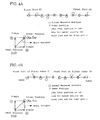
- Figs. 1A to 1C show a ribbon-shaped optical fiber multi-core line for manufacturing a fiber array of the half pitch type.
- Fig. 1A there are prepared two 12-core ribbon-shaped optical fibers 1 and 2, which are laid one over the other.
- jackets 1a and 2a are then removed to form a 24-core ribbon-shaped fiber, in which the upper and lower bare fibers are alternately arrayed in one row in the V-grooves of a V-shaped substrate.
- These 24-core ribbon-shaped fibers are prepared by two to form a fiber array as a 48-core ribbon-shaped fiber, as shown in Figs. 2A to 2C.
- the bare fibers on the outermost side in the array direction and the continuous jacketed fibers are then used as dummy fibers 3 and 3 for transmitting no optical signal.
- the symbols "x" appearing in the shown fiber cores are designations for discriminating the ribbon-shaped optical fibers 1 and 2 and not designations for the transmission direction.
- the dummy fibers 3 and 3 are the bare fibers and the ribbon fiber portion which has the fiber array of the entire length in the fiber longitudinal direction at least between end edges 3b and 3c of the fiber array and which is clamped by a jacket housing plate. As shown in Fig. 1C, however, it is needless to say that the dummy fibers 3 and 3 may include the ribbon fiber portion continuing to the outside of the fiber array.
- Fig. 2A is a front elevation
- Fig. 28 is a side elevation
- Fig. 2C is a top plan view.
- the multi-core line having forty eight cores is shown to have a reduced number of cores, because its width is too large.
- the two ribbon-shaped optical fibers 1 and 2 are bare at their leading ends, and the bare fibers 11 and 21 are fitted in the V-grooves of a V-Grooved substrate 4 and are adhered and fixed downward by a holding plate 5. Moreover, the jackets of the ribbon-shaped optical fibers 1 and 2 are adhered and fixed in the V-shaped substrate 4 by a jacket housing plate 6. Furthermore, the bare fibers 11 and 21, as located at the position of a relaxation portion 7a between the V-shaped substrate 4 and the jacket housing plate 6, are covered with an adhesive 7.
- the dummy fibers 3 and 3 on the outermost sides of the bare fibers 11 and 21 contact at their portions, as enclosed by an ellipse B, with the end edges of the V-grooves. Thus, they are subject to the displacements of the pitches of the jacket portions as a stress from the outer side. Therefore, no stress is applied to the bare fibers on the inner side for transmitting optical signals. Even if the dummy fibers 3 should be broken by a high stress, moreover, the whole stress is not applied to the fibers located just inside of the broken dummy fibers and next the outer side, because the bare portions are covered and fixed by the adhesive 7. As a result, the stress is dispersed by the adhesive into small ones so that a possibility of causing a problem is drastically lowered.
- Fig. 3 is a side elevation of a waveguide device according to the present invention.
- a waveguide device 20 is prepared by connecting a fiber array 8 optically with a waveguide chip 9 and by sealing the connected ones in a package 10.
- the leading ends of the unjacket bare fibers 11 of the ribbon-shaped optical fiber multi-core line 1 are arrayed in the V-grooves of the V-shaped substrate 4.
- the package 10 is frequently formed into a box shape having a cover on its upper face, but its sealing means is not limited.
- This fiber array 8 in which the leading ends of the unjacket bare fibers 11 of the ribbon-shaped optical fiber multi-core line 1 are arrayed in the V-grooves of the V-shaped substrate 4, does not use the jacket housing plate 6 for adhering and fixing the jackets, unlike the shape shown in Figs. 2A to 2C. Instead, the jacket of the ribbon-shaped optical fiber multi-core line 1 is fixed by clamping it between the box and the cover of the package, for example.
- these dummy fibers to be used can be at least as the outermost ones of the array of the unjacket bare fibers 11 of the ribbon-shaped optical fiber multi-core line 1, and can have a length equal to the fibers used as the inner signal lines.
- the waveguide device has to be provided with the dummy fibers from the fiber array 8 to at least the inner face 10a of the package for fixing the jackets. Even in the waveguide device in which the leading ends of the bare fibers but not the jackets are fixed in the V-grooves of the fiber array and in which the jackets are fixed by the package to fix the fiber multi-core line, therefore, no optical signal is transmitted to at least the outermost side fibers.
- the outermost optical fibers absorb the bending stress or the like to be applied to the remaining bare fibers. Additionally, even if the bare fibers on the outermost sides are broken in rare cases by the severe vibrations or the like of the outside is placed, no optical signal has been transmitted. Therefore, the loss in the signals is not increased and so that the fiber array is not broken. Thus the fiber array is excellent in a long stability.
- the positional adjustment is not required since the 1st to 4th cores and the 45th to 48th cores are dummy fibers.
- the ideal positions for the sixth core to the forty third core have to be calculated with reference to their inner fifth and forty fourth cores, and the adjustment has to be made to attain the ideal positions.
- the fiber positions are measured with reference to the fifth core and the forty fourth core.
- the necessary operations are only to measure the fiber positions with reference to a first port 71 and a final port 79, as located on the two ends of the signal fibers having the dummy fibers on the two sides, thereby to raise the working efficiency.
- the 48-core fiber array as shown in Figs. 1A to 1C by omitting the central portion, was subjected to an endurance test according to the bell core standards. This test was conducted for one ribbon fiber having four dummy fibers, i.e., two fibers on the two outer sides, at a temperature condition of -40 °C to 85 °C and for one trial of 1,000 cycles.
- a fiber array in which bare fibers, as unjacket, of a ribbon-shaped optical fiber multi-core line are arrayed in V-grooves of a V-shaped substrate. Dummy fibers are disposed on at least the outermost sides of the array of said bare fibers, and disposed over at least the entire length of the fiber array. Therefore, no optical signal is transmitted to at least the outermost side fibers of the ribbon-shaped optical fibermulti-core line having the optical fibers arrayed in the V-grooves. As a result, the outermost optical fibers absorb the bending stress or the like to be applied to the remaining bare fibers.
- a waveguide device in which a fiber array having unclad bare fibers of a ribbon-shaped optical fiber multi-core line arrayed in V-grooves of a V-shaped substrate is optically connected to a waveguide chip and is sealed in a package. Dummy fibers for transmitting no optical signal are disposed on at least the outermost sides of the array of said bare fibers, and disposed from said fiber array to at least the inner face of the package for fixing the jackets.
- the waveguide device in which the leading ends of the bare fibers but not the jackets are fixed in the V-grooves of the fiber array and in which the jackets are fixed by the package to fix the fiber multi-core line, no optical signal is transmitted to at least the outermost side fibers.
- the outermost optical fibers absorb the bending stress or the like to be applied to the remaining bare fibers.
- no optical signal is transmitted.
- the loss in the signals is not increased and so that the bare fibers are not broken.
- the device is excellent in a long stability.
Landscapes
- Physics & Mathematics (AREA)
- General Physics & Mathematics (AREA)
- Optics & Photonics (AREA)
- Mechanical Coupling Of Light Guides (AREA)
- Optical Couplings Of Light Guides (AREA)
Applications Claiming Priority (4)
| Application Number | Priority Date | Filing Date | Title |
|---|---|---|---|
| JP2000380900 | 2000-12-14 | ||
| JP2000380900 | 2000-12-14 | ||
| JP2001346559A JP3697580B2 (ja) | 2000-12-14 | 2001-11-12 | ファイバアレイ及び導波路デバイス |
| JP2001346559 | 2001-11-12 |
Publications (3)
| Publication Number | Publication Date |
|---|---|
| EP1215517A2 true EP1215517A2 (de) | 2002-06-19 |
| EP1215517A3 EP1215517A3 (de) | 2004-10-13 |
| EP1215517B1 EP1215517B1 (de) | 2009-02-18 |
Family
ID=26605854
Family Applications (1)
| Application Number | Title | Priority Date | Filing Date |
|---|---|---|---|
| EP01310469A Expired - Lifetime EP1215517B1 (de) | 2000-12-14 | 2001-12-14 | Verwendung einer optischen Fasermatrixanordnung |
Country Status (8)
| Country | Link |
|---|---|
| US (1) | US6768861B2 (de) |
| EP (1) | EP1215517B1 (de) |
| JP (1) | JP3697580B2 (de) |
| KR (1) | KR20020046950A (de) |
| CN (1) | CN1188723C (de) |
| CA (1) | CA2364896A1 (de) |
| DE (1) | DE60137674D1 (de) |
| TW (1) | TW552436B (de) |
Cited By (2)
| Publication number | Priority date | Publication date | Assignee | Title |
|---|---|---|---|---|
| WO2005040879A1 (en) * | 2003-10-16 | 2005-05-06 | 3M Innovative Properties Company | Optical interconnect device |
| CN107237261A (zh) * | 2017-05-22 | 2017-10-10 | 北京恒润生工程科技有限公司 | 基于botdr的智能拉索及其制备方法 |
Families Citing this family (12)
| Publication number | Priority date | Publication date | Assignee | Title |
|---|---|---|---|---|
| CN100359352C (zh) * | 2004-11-26 | 2008-01-02 | 李德建 | 光纤的胶合固定方法以及配套使用的填充棒 |
| CN100356221C (zh) * | 2005-12-30 | 2007-12-19 | 武汉海博光技术有限公司 | 光纤阵列组件中光纤排放封装设备 |
| US20080101751A1 (en) * | 2006-10-31 | 2008-05-01 | Luther James P | Multi-fiber ferrule with guard fiber |
| JP4331250B2 (ja) * | 2008-06-27 | 2009-09-16 | 三菱電線工業株式会社 | 光ファイバアレイ |
| US20120275753A1 (en) * | 2011-04-28 | 2012-11-01 | Reinhardt Sherrh C | Fiber assembly with tray feature |
| JPWO2013157245A1 (ja) * | 2012-04-20 | 2015-12-21 | 日本電気株式会社 | 多重光伝送路、光伝送システムおよび光伝送方法 |
| US11156781B2 (en) * | 2013-06-14 | 2021-10-26 | Chiral Photonics, Inc. | Passive aligning optical coupler array |
| US11966091B2 (en) * | 2013-06-14 | 2024-04-23 | Chiral Photonics, Inc. | Multichannel optical coupler array |
| JP6972904B2 (ja) * | 2017-10-19 | 2021-11-24 | 住友電気工業株式会社 | 光ファイバケーブル、光コネクタケーブル、及び、光ファイバケーブルの製造方法 |
| US12210185B2 (en) | 2020-02-24 | 2025-01-28 | Chiral Photonics, Inc. | Wavelength division multiplexers for space division multiplexing (SDM-WDM devices) |
| CN120303591A (zh) * | 2022-11-08 | 2025-07-11 | 康宁研究与开发公司 | 光纤阵列中的纤芯间距控制 |
| US20240385388A1 (en) * | 2023-05-18 | 2024-11-21 | Taiwan Semiconductor Manufacturing Co., Ltd. | Optical Devices and Methods of Manufacture |
Family Cites Families (10)
| Publication number | Priority date | Publication date | Assignee | Title |
|---|---|---|---|---|
| JPS5953315U (ja) * | 1982-10-01 | 1984-04-07 | 日本電気株式会社 | 光フアイバアレイ |
| JPH03155503A (ja) * | 1989-11-14 | 1991-07-03 | Nippon Sheet Glass Co Ltd | 光ファイバ配列体 |
| JPH05264844A (ja) * | 1992-03-24 | 1993-10-15 | Ngk Insulators Ltd | 光ファイバアレイおよびその基板 |
| JP3160407B2 (ja) * | 1993-02-12 | 2001-04-25 | 日本碍子株式会社 | 光ファイバの接続方法 |
| JP3764509B2 (ja) * | 1994-08-26 | 2006-04-12 | 京セラ株式会社 | 光導波路型モジュール |
| JP3273490B2 (ja) * | 1995-09-22 | 2002-04-08 | 日本電信電話株式会社 | 多芯マイクロキャピラリとこれを用いた光導波回路と光ファイバとの接続方法 |
| WO1998005989A1 (en) * | 1996-08-01 | 1998-02-12 | Furukawa Denki Kogyo Kabushiki Kaisha | Multicore optical connector and method of producing the connector |
| EP0985943B1 (de) * | 1998-09-09 | 2006-11-15 | Sumitomo Electric Industries, Ltd. | Verfahren zur Herstellung eines faseroptischen Arrays und Vorrichtung zur Herstellung eines faseroptischen Arrays |
| JP3931940B2 (ja) * | 1998-12-18 | 2007-06-20 | リコープリンティングシステムズ株式会社 | 光ファイバアレイ素子およびその製造方法 |
| JP2002072016A (ja) * | 2000-09-04 | 2002-03-12 | Sumitomo Electric Ind Ltd | 光ファイバアレイおよび光部品 |
-
2001
- 2001-11-12 JP JP2001346559A patent/JP3697580B2/ja not_active Expired - Fee Related
- 2001-12-07 TW TW090130442A patent/TW552436B/zh not_active IP Right Cessation
- 2001-12-11 KR KR1020010078084A patent/KR20020046950A/ko not_active Abandoned
- 2001-12-12 CN CNB011442085A patent/CN1188723C/zh not_active Expired - Fee Related
- 2001-12-12 CA CA002364896A patent/CA2364896A1/en not_active Abandoned
- 2001-12-13 US US10/022,181 patent/US6768861B2/en not_active Expired - Fee Related
- 2001-12-14 EP EP01310469A patent/EP1215517B1/de not_active Expired - Lifetime
- 2001-12-14 DE DE60137674T patent/DE60137674D1/de not_active Expired - Lifetime
Cited By (3)
| Publication number | Priority date | Publication date | Assignee | Title |
|---|---|---|---|---|
| WO2005040879A1 (en) * | 2003-10-16 | 2005-05-06 | 3M Innovative Properties Company | Optical interconnect device |
| US7186031B2 (en) | 2003-10-16 | 2007-03-06 | 3M Innovative Properties Company | Optical interconnect device |
| CN107237261A (zh) * | 2017-05-22 | 2017-10-10 | 北京恒润生工程科技有限公司 | 基于botdr的智能拉索及其制备方法 |
Also Published As
| Publication number | Publication date |
|---|---|
| US20020076190A1 (en) | 2002-06-20 |
| EP1215517B1 (de) | 2009-02-18 |
| TW552436B (en) | 2003-09-11 |
| JP3697580B2 (ja) | 2005-09-21 |
| DE60137674D1 (de) | 2009-04-02 |
| CA2364896A1 (en) | 2002-06-14 |
| JP2002243970A (ja) | 2002-08-28 |
| US6768861B2 (en) | 2004-07-27 |
| EP1215517A3 (de) | 2004-10-13 |
| KR20020046950A (ko) | 2002-06-21 |
| CN1359015A (zh) | 2002-07-17 |
| CN1188723C (zh) | 2005-02-09 |
Similar Documents
| Publication | Publication Date | Title |
|---|---|---|
| US6768861B2 (en) | Fiber array, and waveguide device | |
| KR100418842B1 (ko) | 광 섬유용 수동 정렬 접속부 | |
| EP0859253B1 (de) | Optischer mehrkern-stecker und sein herstellungsverfahren | |
| TWI498615B (zh) | 積體矽光激性主動光學電纜組件、子組合及組合 | |
| US6004042A (en) | Multi-fiber connector | |
| US6859588B2 (en) | Optical fiber block | |
| JP2010211240A (ja) | 複数の光ファイバーを有するデバイス | |
| US20030091289A1 (en) | Planar lightwave circuit module and method for manufacturing the same | |
| JP2003302561A (ja) | 光ファイバ部品およびその製造方法 | |
| US6049646A (en) | Integrated burster multiplexer duplexer device for multicore fibers | |
| JP2005173043A (ja) | 多チャンネル光モジュール | |
| JP5477691B2 (ja) | 光モジュール | |
| JPH10246838A (ja) | 光ファイバアレイ装置 | |
| JP3772929B2 (ja) | 光ファイバ保持部品および光ファイバアレイ | |
| EP1731935A1 (de) | Lwl anordnung | |
| JPH07248424A (ja) | 光ファイバアレイおよび光デバイス | |
| US5649037A (en) | Optical waveguide component and a light signal processing method using the same | |
| JPH09105838A (ja) | 光導波路装置 | |
| WO1997005512A1 (en) | 36 fiber macii chip | |
| WO1997005512A9 (en) | 36 fiber macii chip | |
| JPH0618744A (ja) | 光分岐ユニット及びこのユニットに用いる導波路型光カプラモジュール | |
| JPH1096836A (ja) | 多心光コネクタおよびその製造方法 | |
| KR100315476B1 (ko) | 리본 광섬유 | |
| JP2000221364A (ja) | 多心光コネクタ | |
| US20260110851A1 (en) | Optical connection assembly and method of manufacturing optical connection assembly |
Legal Events
| Date | Code | Title | Description |
|---|---|---|---|
| PUAI | Public reference made under article 153(3) epc to a published international application that has entered the european phase |
Free format text: ORIGINAL CODE: 0009012 |
|
| AK | Designated contracting states |
Kind code of ref document: A2 Designated state(s): AT BE CH CY DE DK ES FI FR GB GR IE IT LI LU MC NL PT SE TR |
|
| AX | Request for extension of the european patent |
Free format text: AL;LT;LV;MK;RO;SI |
|
| PUAL | Search report despatched |
Free format text: ORIGINAL CODE: 0009013 |
|
| AK | Designated contracting states |
Kind code of ref document: A3 Designated state(s): AT BE CH CY DE DK ES FI FR GB GR IE IT LI LU MC NL PT SE TR |
|
| AX | Request for extension of the european patent |
Extension state: AL LT LV MK RO SI |
|
| 17P | Request for examination filed |
Effective date: 20041102 |
|
| 17Q | First examination report despatched |
Effective date: 20041126 |
|
| AKX | Designation fees paid |
Designated state(s): DE FR GB IT |
|
| RTI1 | Title (correction) |
Free format text: USE OF AN OPTICAL FIBER ARRAY |
|
| GRAP | Despatch of communication of intention to grant a patent |
Free format text: ORIGINAL CODE: EPIDOSNIGR1 |
|
| GRAS | Grant fee paid |
Free format text: ORIGINAL CODE: EPIDOSNIGR3 |
|
| RBV | Designated contracting states (corrected) |
Designated state(s): DE FR GB |
|
| GRAA | (expected) grant |
Free format text: ORIGINAL CODE: 0009210 |
|
| AK | Designated contracting states |
Kind code of ref document: B1 Designated state(s): DE FR GB |
|
| REG | Reference to a national code |
Ref country code: GB Ref legal event code: FG4D |
|
| REF | Corresponds to: |
Ref document number: 60137674 Country of ref document: DE Date of ref document: 20090402 Kind code of ref document: P |
|
| PLBE | No opposition filed within time limit |
Free format text: ORIGINAL CODE: 0009261 |
|
| STAA | Information on the status of an ep patent application or granted ep patent |
Free format text: STATUS: NO OPPOSITION FILED WITHIN TIME LIMIT |
|
| 26N | No opposition filed |
Effective date: 20091119 |
|
| REG | Reference to a national code |
Ref country code: FR Ref legal event code: PLFP Year of fee payment: 15 |
|
| PGFP | Annual fee paid to national office [announced via postgrant information from national office to epo] |
Ref country code: GB Payment date: 20151209 Year of fee payment: 15 Ref country code: DE Payment date: 20151208 Year of fee payment: 15 |
|
| PGFP | Annual fee paid to national office [announced via postgrant information from national office to epo] |
Ref country code: FR Payment date: 20151110 Year of fee payment: 15 |
|
| REG | Reference to a national code |
Ref country code: DE Ref legal event code: R119 Ref document number: 60137674 Country of ref document: DE |
|
| GBPC | Gb: european patent ceased through non-payment of renewal fee |
Effective date: 20161214 |
|
| REG | Reference to a national code |
Ref country code: FR Ref legal event code: ST Effective date: 20170831 |
|
| PG25 | Lapsed in a contracting state [announced via postgrant information from national office to epo] |
Ref country code: FR Free format text: LAPSE BECAUSE OF NON-PAYMENT OF DUE FEES Effective date: 20170102 |
|
| PG25 | Lapsed in a contracting state [announced via postgrant information from national office to epo] |
Ref country code: DE Free format text: LAPSE BECAUSE OF NON-PAYMENT OF DUE FEES Effective date: 20170701 Ref country code: GB Free format text: LAPSE BECAUSE OF NON-PAYMENT OF DUE FEES Effective date: 20161214 |