EP1222988A2 - Buse pour appareil de brasage - Google Patents
Buse pour appareil de brasage Download PDFInfo
- Publication number
- EP1222988A2 EP1222988A2 EP02250154A EP02250154A EP1222988A2 EP 1222988 A2 EP1222988 A2 EP 1222988A2 EP 02250154 A EP02250154 A EP 02250154A EP 02250154 A EP02250154 A EP 02250154A EP 1222988 A2 EP1222988 A2 EP 1222988A2
- Authority
- EP
- European Patent Office
- Prior art keywords
- solder
- leads
- wetted
- dipped
- nozzle
- Prior art date
- Legal status (The legal status is an assumption and is not a legal conclusion. Google has not performed a legal analysis and makes no representation as to the accuracy of the status listed.)
- Granted
Links
Images


Classifications
-
- B—PERFORMING OPERATIONS; TRANSPORTING
- B23—MACHINE TOOLS; METAL-WORKING NOT OTHERWISE PROVIDED FOR
- B23K—SOLDERING OR UNSOLDERING; WELDING; CLADDING OR PLATING BY SOLDERING OR WELDING; CUTTING BY APPLYING HEAT LOCALLY, e.g. FLAME CUTTING; WORKING BY LASER BEAM
- B23K1/00—Soldering, e.g. brazing, or unsoldering
- B23K1/08—Soldering by means of dipping in molten solder
- B23K1/085—Wave soldering
-
- B—PERFORMING OPERATIONS; TRANSPORTING
- B23—MACHINE TOOLS; METAL-WORKING NOT OTHERWISE PROVIDED FOR
- B23K—SOLDERING OR UNSOLDERING; WELDING; CLADDING OR PLATING BY SOLDERING OR WELDING; CUTTING BY APPLYING HEAT LOCALLY, e.g. FLAME CUTTING; WORKING BY LASER BEAM
- B23K3/00—Tools, devices or special appurtenances for soldering, e.g. brazing, or unsoldering, not specially adapted for particular methods
- B23K3/06—Solder feeding devices; Solder melting pans
- B23K3/0646—Solder baths
- B23K3/0653—Solder baths with wave generating means, e.g. nozzles, jets, fountains
-
- H—ELECTRICITY
- H05—ELECTRIC TECHNIQUES NOT OTHERWISE PROVIDED FOR
- H05K—PRINTED CIRCUITS; CASINGS OR CONSTRUCTIONAL DETAILS OF ELECTRIC APPARATUS; MANUFACTURE OF ASSEMBLAGES OF ELECTRICAL COMPONENTS
- H05K3/00—Apparatus or processes for manufacturing printed circuits
- H05K3/30—Assembling printed circuits with electric components, e.g. with resistors
- H05K3/32—Assembling printed circuits with electric components, e.g. with resistors electrically connecting electric components or wires to printed circuits
- H05K3/34—Assembling printed circuits with electric components, e.g. with resistors electrically connecting electric components or wires to printed circuits by soldering
- H05K3/3447—Lead-in-hole components
-
- H—ELECTRICITY
- H05—ELECTRIC TECHNIQUES NOT OTHERWISE PROVIDED FOR
- H05K—PRINTED CIRCUITS; CASINGS OR CONSTRUCTIONAL DETAILS OF ELECTRIC APPARATUS; MANUFACTURE OF ASSEMBLAGES OF ELECTRICAL COMPONENTS
- H05K3/00—Apparatus or processes for manufacturing printed circuits
- H05K3/30—Assembling printed circuits with electric components, e.g. with resistors
- H05K3/32—Assembling printed circuits with electric components, e.g. with resistors electrically connecting electric components or wires to printed circuits
- H05K3/34—Assembling printed circuits with electric components, e.g. with resistors electrically connecting electric components or wires to printed circuits by soldering
- H05K3/3465—Application of solder
- H05K3/3468—Application of molten solder, e.g. dip soldering
Definitions
- the present invention relates to soldering apparatus, and more particularly to a nozzle for use in a dip soldering process
- soldering apparatus is described in EP-A-212 911, EP-A-481 710 and EP-A-564 096 for example.
- solder is pumped from a bath upwards through a nozzle, overflowing the nozzle outlet and returning to the bath.
- a component or circuit board to be soldered is lowered to dip the leads into the surface of solder at the nozzle outlet.
- Different sizes and shapes of nozzle are provided to suit the particular component or circuit board layout.
- Another approach is to temporarily reduce or stop the flow of solder through the nozzle, so that the solder surface falls away from the circuit board. This does not require rotation of the board, but it is not particularly successful in avoiding solder bridging.
- a plate or other member which is wetted by the solder is positioned between the leads which are being soldered.
- the plate may be elongate and extend between two rows of leads.
- the board is usually brought down on to the solder surface or close thereto.
- the plate or wetted member will generally lie just below the solder surface for the initial dipping operation.
- solder surface itself may then be lowered below the upper edge of the plate. This draws the solder away from the joints, reducing the likelihood of solder bridging.
- the plate or the like may be raised with the board as the board is lifted away from the solder surface, plate serving to break through the solder surface and so draw solder down towards the plate.
- the shape and positioning of the plate or other wetted member can be tailored to suit the components being soldered.
- a soldering machine is set up as part of a production line to solder a run of identical products, and nozzles, for delivering the solder to the underside of the circuit board for example, will be designed to fit around the leads being solder.
- the wetted member preferably extends between the rows. It will serve to prevent bridging between the rows and also between adjacent leads in a row.
- a wetted member could be positioned to each outer side of the array. In this latter case, the wetted member could be formed by the nozzle walls themselves.
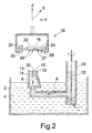
- a bath 2 contains molten solder 4, which is heated by a heater, not shown.
- the bath may be covered and/or shrouded in an inert atmosphere such as nitrogen to reduce the formation of dross (oxidised solder).
- a nozzle 6 is supported on a tubular arm 8 which extends from an impeller housing 10.
- An impeller 12 is rotated by an electric motor, not shown, to pump solder 4 through arm 8 into nozzle 6.
- the speed of impeller 12 is adjusted so that solder overflows an upper edge 13 defining an outlet 14 of nozzle 6. This ensures that a fresh solder surface 15 is continuously provided at the nozzle outlet 14.
- a printed circuit board 16 is held by a component holder 18 which translates the board 16 in the horizontal plane X, Y and also lowers the board in the vertical direction Z.
- Circuit board 16 has components 20, 22, 24 having leads 25, 26, 27 which extend through the board and are to be soldered to printed circuit tracks (not shown) on the underside 28 of the board 16.
- the board 16 is, optionally, first passed through a fluxing station where flux is sprayed onto the areas to be soldered.
- the board is then positioned over the nozzle 6 and lowered, in the Z direction, to dip leads 26 into the solder surface 15 at the nozzle outlet 14.
- the board 16 will be lowered until it just presses on the solder surface 15. This will help ensure that solder passes into any through holes in the board and is supplied to the junction between the leads 26 and the printed circuit tracks.
- the board 16 is raised and/or solder surface 15 is lowered. Excess solder will be drawn away from the underside 28 of the board 16 by surface tension. The speed of impeller 12 may be reduced to cause the solder surface 15 to drop away from the board.
- the board 16 When the board 16 has several components to be soldered, the board may be re-positioned to solder the other component leads, additional nozzles may be provided, and/or a larger nozzle may be provided to accommodate leads from more than one component. With closely spaced leads, there is a tendency for excess solder to remain on the board, bridging the leads, as illustrated by leads 27 which are shown as having been soldered already with solder fillets 29. This is very undesirable.
- the nozzle 6 may be raised towards the board or component being soldered as described in EP-A-212 911.
- the solder may be held stationary at the nozzle outlet (i.e. not overflowing the nozzle outlet) or the nozzle may be in the form of a pot which is raised through the surface of the solder in the bath as described in EP-A-481 710.
- US 5 611 480 describes a way of overcoming the problem of solder bridging by rotating the board as it leaves the solder surface.
- FIG. 2 shows an embodiment of the present invention, which is a modification of the apparatus of Figure 1. Like parts have been given like reference numerals.
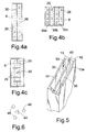
- a plate 30 is positioned in the nozzle outlet 14.
- Plate 30 is of a material which is wetted by the solder 4, for example of iron.
- solder 4 for example of iron.
- the leads 26 pass either side of the plate 30. It is believed that the plate 30 functions to draw more solder away from the underside 28 of the board. Plate 30 is particularly effective if, before the leads 26 are withdrawn, or withdrawn completely, from the solder surface 15, the surface 15 is lowered to below the upper edge 32 of the plate 30, as will be described in more detail with reference to Figure 3.
- the upper edge 32 of plate 30 is at the same level as the upper edge of the nozzle 6, defining the nozzle outlet 14.
- solder 4 cover the plate 30 during the initial dipping operation, i.e. when the solder is flowing, as illustrated in Figure 3a.
- the plate upper edge 32 may be level with the cut away portion.
- the board 16 has been lowered so that the underside 28 of the board 16 just touches the solder surface 15, although it may be stopped just short of this. Solder 4 will flow up the leads 26 to touch the tracks 33 on the underside 28 of the board 16.
- the speed of impeller 6 has been lowered, to drop the solder surface 15 to below the ends 31 of the leads 26.
- solder surface 15 falls, excess solder is drawn away from the leads 26.
- plate 30 By having a wetted surface in the vicinity of the leads 26, provided by plate 30, it is possible to ensure that excess solders not held between the leads 26, which would cause solder bridging.
- the plate 30 is positioned so that it extends below the ends of the leads, to be interacting with the solder surface 15 as the solder leaves the ends 31 of the leads.
- the amount of solder retained by the leads 26 can be adjusted.
- the board 16 may be raised to withdraw the leads 26 from the solder surface 15, as well as lowering the surface 15. However, it is thought to be necessary for the plate 30 to project through the surface 15 at the time the leads 26 clear the surface 15.
- nozzle outlet 14 will be tailored to suit the array of leads which are to be soldered. Similar the plate(s) 30 may be tailored to suit the array of leads.
- this shows two rows of leads and a plate 30 extending between them.
- Figure 5 shows a perspective view of the nozzle outlet 14, with plate 30 supported in rebates 40 in the nozzle side walls 42.
- wetted plate 30 may be replaced or supplemented by a wetted surface 50 at the nozzle outlet 14. This may be particularly suitable when soldering a single row of closely spaced leads, as illustrated in Figure 6.
- wetted member has been shown as extending along the length of a row of leads, it could be provided only at or near the end of a row, for example, in order to target those areas where solder bridging is most prone to occur. Also, while vertical movement of the circuit board is shown, the system may also be used when the board is rotated.
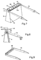
- Figure 7 shows a second embodiment in which the wetted member is movable so as to rise through the solder surface 15 as the board 16 is lifted.
- the wetted member 68 is in the form of a rod 70 carrying pins 72 which, in use, extend up between leads 26 on the circuit board (see Figure 8).
- the rod 70 slides in slots 74 in sidewalls 76 of the nozzle 6 and is carried on pivot arms 78. Arms 78 may be biassed or electrically controlled to raise and lower the wetted member 68.
- the wetted member 68 has a shape similar to member 30 of Figure 4c.
Landscapes
- Engineering & Computer Science (AREA)
- Mechanical Engineering (AREA)
- Electric Connection Of Electric Components To Printed Circuits (AREA)
- Molten Solder (AREA)
- Mechanical Treatment Of Semiconductor (AREA)
- Grinding And Polishing Of Tertiary Curved Surfaces And Surfaces With Complex Shapes (AREA)
- Finish Polishing, Edge Sharpening, And Grinding By Specific Grinding Devices (AREA)
Applications Claiming Priority (2)
| Application Number | Priority Date | Filing Date | Title |
|---|---|---|---|
| GB0100626A GB2371006B (en) | 2001-01-10 | 2001-01-10 | Nozzle for soldering apparatus |
| GB0100626 | 2001-01-10 |
Publications (3)
| Publication Number | Publication Date |
|---|---|
| EP1222988A2 true EP1222988A2 (fr) | 2002-07-17 |
| EP1222988A3 EP1222988A3 (fr) | 2003-02-12 |
| EP1222988B1 EP1222988B1 (fr) | 2008-06-11 |
Family
ID=9906572
Family Applications (1)
| Application Number | Title | Priority Date | Filing Date |
|---|---|---|---|
| EP02250154A Expired - Lifetime EP1222988B1 (fr) | 2001-01-10 | 2002-01-10 | Procédé et dispositif pour le soudage par trempage |
Country Status (5)
| Country | Link |
|---|---|
| US (1) | US7650851B2 (fr) |
| EP (1) | EP1222988B1 (fr) |
| AT (1) | ATE397992T1 (fr) |
| DE (2) | DE60227015D1 (fr) |
| GB (1) | GB2371006B (fr) |
Families Citing this family (10)
| Publication number | Priority date | Publication date | Assignee | Title |
|---|---|---|---|---|
| US20050069668A1 (en) * | 2003-09-30 | 2005-03-31 | Daodang Hung Q. | Disk lubricant tank insert to suppress lubricant surface waves |
| US7358856B2 (en) * | 2004-03-18 | 2008-04-15 | Savi Technology, Inc. | Two-phase commit synchronizing seal state |
| JP4370225B2 (ja) * | 2004-08-19 | 2009-11-25 | 住友電装株式会社 | プリント基板への端子実装方法、該方法で形成した端子実装プリント基板および該端子実装プリント基板を収容している電気接続箱 |
| JP5884058B2 (ja) * | 2010-02-26 | 2016-03-15 | パナソニックIpマネジメント株式会社 | 半田付け装置 |
| DE102013110731B3 (de) * | 2013-09-27 | 2014-11-06 | Ersa Gmbh | Trennstreifen-Anordnung für Lötdüse, sowie Lötdüseneinrichtung zum selektiven Wellenlöten |
| DE102018105388A1 (de) * | 2018-03-08 | 2019-09-12 | Ersa Gmbh | Lötdüse und Lötanlage |
| US20190337075A1 (en) * | 2018-05-01 | 2019-11-07 | Artos Engineering Company | Systems and devices for improved solder dispensing |
| JP7340388B2 (ja) * | 2019-08-21 | 2023-09-07 | 株式会社デンソーテン | はんだ付け装置 |
| EP3785838B1 (fr) * | 2019-08-27 | 2022-07-20 | Illinois Tool Works, Inc. | Ensemble de soudure, procédé et utilisation |
| EP3785837B1 (fr) * | 2019-08-27 | 2024-10-02 | Illinois Tool Works, Inc. | Buse, système et procédé |
Family Cites Families (24)
| Publication number | Priority date | Publication date | Assignee | Title |
|---|---|---|---|---|
| US2770875A (en) * | 1952-06-09 | 1956-11-20 | Motorola Inc | Soldering machine |
| US3056370A (en) * | 1955-10-14 | 1962-10-02 | Fry S Metal Foundries Ltd | Apparatus for soldering |
| US3196829A (en) * | 1963-02-21 | 1965-07-27 | Fry S Metal Foundries Ltd | Soldering machines |
| US3151592A (en) * | 1963-05-20 | 1964-10-06 | Howard W Wegener | Sump and nozzle for soldering machines |
| US3303983A (en) | 1964-11-12 | 1967-02-14 | Gen Dynamics Corp | Ultrasonic soldering apparatus |
| US3565319A (en) * | 1967-05-15 | 1971-02-23 | Banner Ind Inc | Apparatus for application of solder to circuit boards |
| US4527731A (en) * | 1983-03-31 | 1985-07-09 | At&T Technologies, Inc. | Method and apparatus for applying stripes of solder to articles |
| US4545520A (en) * | 1983-08-30 | 1985-10-08 | At&T Technologies, Inc. | Method and system for soldering insulation coated parts |
| EP0147000A1 (fr) * | 1983-12-15 | 1985-07-03 | Hollis Automation Inc. | Système I à souder par ondes destiné à la fabrication en masse |
| US4684056A (en) * | 1985-05-03 | 1987-08-04 | Electrovert Limited | Vibratory wave soldering |
| US4739919A (en) * | 1987-06-15 | 1988-04-26 | Northern Telecom Limited | Masking of circuit boards for wave soldering |
| MY104651A (en) | 1988-08-31 | 1994-05-31 | Matsushita Electric Industrial Co Ltd | An automatic jet soldering apparatus |
| US5203489A (en) * | 1991-12-06 | 1993-04-20 | Electrovert Ltd. | Gas shrouded wave soldering |
| US5227589A (en) * | 1991-12-23 | 1993-07-13 | Motorola, Inc. | Plated-through interconnect solder thief |
| US5611480A (en) * | 1992-03-03 | 1997-03-18 | Pillarhouse International Limited | Soldering process |
| US5679927A (en) * | 1993-05-13 | 1997-10-21 | Communications Technology Corporation | Buried service wire closure |
| US5604333A (en) * | 1994-11-30 | 1997-02-18 | Intel Corporation | Process and structure for a solder thief on circuit boards |
| DE19506874C1 (de) * | 1995-02-16 | 1996-04-25 | Ersa Loettechnik Gmbh | Schwall-Lötdüse |
| US5679929A (en) * | 1995-07-28 | 1997-10-21 | Solectron Corporqtion | Anti-bridging pads for printed circuit boards and interconnecting substrates |
| JPH09107181A (ja) * | 1995-08-07 | 1997-04-22 | Nippon Superia Shiya:Kk | 噴流式はんだ付け装置 |
| JPH09323165A (ja) * | 1996-06-04 | 1997-12-16 | Sharp Corp | 噴流半田槽ノズル |
| JPH1070360A (ja) * | 1996-08-28 | 1998-03-10 | Toshiba Corp | 半田付装置 |
| GB9703790D0 (en) * | 1997-02-24 | 1997-04-16 | Pillarhouse Int Ltd | Soldering apparatus |
| GB2360237B (en) * | 2000-03-16 | 2003-09-03 | Evenoak Ltd | Nozzle for soldering apparatus |
-
2001
- 2001-01-10 GB GB0100626A patent/GB2371006B/en not_active Expired - Fee Related
-
2002
- 2002-01-10 DE DE60227015T patent/DE60227015D1/de not_active Expired - Fee Related
- 2002-01-10 US US10/044,798 patent/US7650851B2/en not_active Expired - Fee Related
- 2002-01-10 DE DE20200554U patent/DE20200554U1/de not_active Expired - Lifetime
- 2002-01-10 EP EP02250154A patent/EP1222988B1/fr not_active Expired - Lifetime
- 2002-01-10 AT AT02250154T patent/ATE397992T1/de not_active IP Right Cessation
Also Published As
| Publication number | Publication date |
|---|---|
| EP1222988B1 (fr) | 2008-06-11 |
| GB2371006B (en) | 2005-05-04 |
| DE20200554U1 (de) | 2002-05-29 |
| US20020110636A1 (en) | 2002-08-15 |
| GB0100626D0 (en) | 2001-02-21 |
| ATE397992T1 (de) | 2008-07-15 |
| US7650851B2 (en) | 2010-01-26 |
| DE60227015D1 (de) | 2008-07-24 |
| GB2371006A (en) | 2002-07-17 |
| EP1222988A3 (fr) | 2003-02-12 |
Similar Documents
| Publication | Publication Date | Title |
|---|---|---|
| EP1222988B1 (fr) | Procédé et dispositif pour le soudage par trempage | |
| US5402563A (en) | Apparatus for removing electronic device from printed circuit board | |
| US6705506B1 (en) | Inert atmosphere soldering apparatus | |
| NL1017843C2 (nl) | Inrichting voor selectief solderen. | |
| US4709846A (en) | Apparatus for the continuous hot tinning of printed circuit boards | |
| US4410126A (en) | Mass soldering system | |
| US4401253A (en) | Mass soldering system | |
| EP2611564B1 (fr) | Buse de brassage servant à acheminer de la brasure fondue à la face inférieure d'une carte de circuits imprimés | |
| US6364195B1 (en) | Brazing Apparatus | |
| JP4634574B2 (ja) | 局所はんだ付け装置および局所はんだ付け方法 | |
| JPS63193595A (ja) | プリント基板組立体のはんだ付方法および装置 | |
| CA2192864A1 (fr) | Appareil pour le soudage en atmosphere inerte | |
| US4776508A (en) | Electronic component lead tinning device | |
| US4410127A (en) | Method of soldering pins to printed circuit boards, and soldering bath for this method | |
| GB1602779A (en) | Methods and apparatus for mass soldering of printed circuit boards | |
| CA1120603A (fr) | Appareil pour souder les composants sur les cartes a circuits imprimes | |
| JPS595064B2 (ja) | プリント基板のはんだ付け装置 | |
| JP3860355B2 (ja) | 半田バンプの形成方法 | |
| JP2002305372A (ja) | 部分半田付け装置及び方法 | |
| WO2010069066A1 (fr) | Appareil et procédé de brasage | |
| JP3590894B2 (ja) | 自動半田付け方法及び自動半田付け装置 | |
| JP3771676B2 (ja) | 局所はんだ付け装置 | |
| JP2001347366A (ja) | 局所はんだ付け装置 | |
| CA1091102A (fr) | Systeme de soudure a onde de masse | |
| USRE32982E (en) | Mass soldering system |
Legal Events
| Date | Code | Title | Description |
|---|---|---|---|
| PUAI | Public reference made under article 153(3) epc to a published international application that has entered the european phase |
Free format text: ORIGINAL CODE: 0009012 |
|
| AK | Designated contracting states |
Kind code of ref document: A2 Designated state(s): AT BE CH CY DE DK ES FI FR GB GR IE IT LI LU MC NL PT SE TR |
|
| AX | Request for extension of the european patent |
Free format text: AL;LT;LV;MK;RO;SI |
|
| PUAL | Search report despatched |
Free format text: ORIGINAL CODE: 0009013 |
|
| AK | Designated contracting states |
Designated state(s): AT BE CH CY DE DK ES FI FR GB GR IE IT LI LU MC NL PT SE TR |
|
| AX | Request for extension of the european patent |
Extension state: AL LT LV MK RO SI |
|
| 17P | Request for examination filed |
Effective date: 20030807 |
|
| AKX | Designation fees paid |
Designated state(s): AT BE CH CY DE DK ES FI FR GB GR IE IT LI LU MC NL PT SE TR |
|
| 17Q | First examination report despatched |
Effective date: 20050203 |
|
| RTI1 | Title (correction) |
Free format text: DIP SOLDERING METHOD AND APPARATUS |
|
| GRAP | Despatch of communication of intention to grant a patent |
Free format text: ORIGINAL CODE: EPIDOSNIGR1 |
|
| GRAS | Grant fee paid |
Free format text: ORIGINAL CODE: EPIDOSNIGR3 |
|
| GRAA | (expected) grant |
Free format text: ORIGINAL CODE: 0009210 |
|
| AK | Designated contracting states |
Kind code of ref document: B1 Designated state(s): AT BE CH CY DE DK ES FI FR GB GR IE IT LI LU MC NL PT SE TR |
|
| REG | Reference to a national code |
Ref country code: GB Ref legal event code: FG4D |
|
| REG | Reference to a national code |
Ref country code: CH Ref legal event code: EP |
|
| REF | Corresponds to: |
Ref document number: 60227015 Country of ref document: DE Date of ref document: 20080724 Kind code of ref document: P |
|
| REG | Reference to a national code |
Ref country code: IE Ref legal event code: FG4D |
|
| PG25 | Lapsed in a contracting state [announced via postgrant information from national office to epo] |
Ref country code: FI Free format text: LAPSE BECAUSE OF FAILURE TO SUBMIT A TRANSLATION OF THE DESCRIPTION OR TO PAY THE FEE WITHIN THE PRESCRIBED TIME-LIMIT Effective date: 20080611 |
|
| PG25 | Lapsed in a contracting state [announced via postgrant information from national office to epo] |
Ref country code: AT Free format text: LAPSE BECAUSE OF FAILURE TO SUBMIT A TRANSLATION OF THE DESCRIPTION OR TO PAY THE FEE WITHIN THE PRESCRIBED TIME-LIMIT Effective date: 20080611 |
|
| PG25 | Lapsed in a contracting state [announced via postgrant information from national office to epo] |
Ref country code: ES Free format text: LAPSE BECAUSE OF FAILURE TO SUBMIT A TRANSLATION OF THE DESCRIPTION OR TO PAY THE FEE WITHIN THE PRESCRIBED TIME-LIMIT Effective date: 20080922 Ref country code: SE Free format text: LAPSE BECAUSE OF FAILURE TO SUBMIT A TRANSLATION OF THE DESCRIPTION OR TO PAY THE FEE WITHIN THE PRESCRIBED TIME-LIMIT Effective date: 20080911 Ref country code: PT Free format text: LAPSE BECAUSE OF FAILURE TO SUBMIT A TRANSLATION OF THE DESCRIPTION OR TO PAY THE FEE WITHIN THE PRESCRIBED TIME-LIMIT Effective date: 20081111 |
|
| PG25 | Lapsed in a contracting state [announced via postgrant information from national office to epo] |
Ref country code: BE Free format text: LAPSE BECAUSE OF FAILURE TO SUBMIT A TRANSLATION OF THE DESCRIPTION OR TO PAY THE FEE WITHIN THE PRESCRIBED TIME-LIMIT Effective date: 20080611 |
|
| PLBE | No opposition filed within time limit |
Free format text: ORIGINAL CODE: 0009261 |
|
| STAA | Information on the status of an ep patent application or granted ep patent |
Free format text: STATUS: NO OPPOSITION FILED WITHIN TIME LIMIT |
|
| PG25 | Lapsed in a contracting state [announced via postgrant information from national office to epo] |
Ref country code: DK Free format text: LAPSE BECAUSE OF FAILURE TO SUBMIT A TRANSLATION OF THE DESCRIPTION OR TO PAY THE FEE WITHIN THE PRESCRIBED TIME-LIMIT Effective date: 20080611 |
|
| 26N | No opposition filed |
Effective date: 20090312 |
|
| PGFP | Annual fee paid to national office [announced via postgrant information from national office to epo] |
Ref country code: DE Payment date: 20090129 Year of fee payment: 8 Ref country code: NL Payment date: 20090125 Year of fee payment: 8 |
|
| PGFP | Annual fee paid to national office [announced via postgrant information from national office to epo] |
Ref country code: GB Payment date: 20090128 Year of fee payment: 8 |
|
| PG25 | Lapsed in a contracting state [announced via postgrant information from national office to epo] |
Ref country code: IT Free format text: LAPSE BECAUSE OF FAILURE TO SUBMIT A TRANSLATION OF THE DESCRIPTION OR TO PAY THE FEE WITHIN THE PRESCRIBED TIME-LIMIT Effective date: 20080611 Ref country code: MC Free format text: LAPSE BECAUSE OF NON-PAYMENT OF DUE FEES Effective date: 20090131 |
|
| REG | Reference to a national code |
Ref country code: CH Ref legal event code: PL |
|
| PG25 | Lapsed in a contracting state [announced via postgrant information from national office to epo] |
Ref country code: LI Free format text: LAPSE BECAUSE OF NON-PAYMENT OF DUE FEES Effective date: 20090131 Ref country code: CH Free format text: LAPSE BECAUSE OF NON-PAYMENT OF DUE FEES Effective date: 20090131 |
|
| REG | Reference to a national code |
Ref country code: FR Ref legal event code: ST Effective date: 20091030 |
|
| PG25 | Lapsed in a contracting state [announced via postgrant information from national office to epo] |
Ref country code: IE Free format text: LAPSE BECAUSE OF NON-PAYMENT OF DUE FEES Effective date: 20090110 |
|
| PG25 | Lapsed in a contracting state [announced via postgrant information from national office to epo] |
Ref country code: FR Free format text: LAPSE BECAUSE OF NON-PAYMENT OF DUE FEES Effective date: 20090202 |
|
| REG | Reference to a national code |
Ref country code: NL Ref legal event code: V1 Effective date: 20100801 |
|
| GBPC | Gb: european patent ceased through non-payment of renewal fee |
Effective date: 20100110 |
|
| PG25 | Lapsed in a contracting state [announced via postgrant information from national office to epo] |
Ref country code: GR Free format text: LAPSE BECAUSE OF FAILURE TO SUBMIT A TRANSLATION OF THE DESCRIPTION OR TO PAY THE FEE WITHIN THE PRESCRIBED TIME-LIMIT Effective date: 20080912 Ref country code: NL Free format text: LAPSE BECAUSE OF NON-PAYMENT OF DUE FEES Effective date: 20100801 |
|
| PG25 | Lapsed in a contracting state [announced via postgrant information from national office to epo] |
Ref country code: DE Free format text: LAPSE BECAUSE OF NON-PAYMENT OF DUE FEES Effective date: 20100803 |
|
| PG25 | Lapsed in a contracting state [announced via postgrant information from national office to epo] |
Ref country code: GB Free format text: LAPSE BECAUSE OF NON-PAYMENT OF DUE FEES Effective date: 20100110 |
|
| PG25 | Lapsed in a contracting state [announced via postgrant information from national office to epo] |
Ref country code: LU Free format text: LAPSE BECAUSE OF NON-PAYMENT OF DUE FEES Effective date: 20090110 |
|
| PG25 | Lapsed in a contracting state [announced via postgrant information from national office to epo] |
Ref country code: TR Free format text: LAPSE BECAUSE OF FAILURE TO SUBMIT A TRANSLATION OF THE DESCRIPTION OR TO PAY THE FEE WITHIN THE PRESCRIBED TIME-LIMIT Effective date: 20080611 |
|
| PG25 | Lapsed in a contracting state [announced via postgrant information from national office to epo] |
Ref country code: CY Free format text: LAPSE BECAUSE OF FAILURE TO SUBMIT A TRANSLATION OF THE DESCRIPTION OR TO PAY THE FEE WITHIN THE PRESCRIBED TIME-LIMIT Effective date: 20080611 |