JP4134004B2 - 高周波モジュール - Google Patents
高周波モジュール Download PDFInfo
- Publication number
- JP4134004B2 JP4134004B2 JP2004329996A JP2004329996A JP4134004B2 JP 4134004 B2 JP4134004 B2 JP 4134004B2 JP 2004329996 A JP2004329996 A JP 2004329996A JP 2004329996 A JP2004329996 A JP 2004329996A JP 4134004 B2 JP4134004 B2 JP 4134004B2
- Authority
- JP
- Japan
- Prior art keywords
- conductor layer
- transmission
- circuit
- reception
- conductor
- Prior art date
- Legal status (The legal status is an assumption and is not a legal conclusion. Google has not performed a legal analysis and makes no representation as to the accuracy of the status listed.)
- Expired - Fee Related
Links
Images




Classifications
-
- H—ELECTRICITY
- H05—ELECTRIC TECHNIQUES NOT OTHERWISE PROVIDED FOR
- H05K—PRINTED CIRCUITS; CASINGS OR CONSTRUCTIONAL DETAILS OF ELECTRIC APPARATUS; MANUFACTURE OF ASSEMBLAGES OF ELECTRICAL COMPONENTS
- H05K1/00—Printed circuits
- H05K1/02—Details
- H05K1/0213—Electrical arrangements not otherwise provided for
- H05K1/0216—Reduction of cross-talk, noise or electromagnetic interference
- H05K1/0218—Reduction of cross-talk, noise or electromagnetic interference by printed shielding conductors, ground planes or power plane
-
- H—ELECTRICITY
- H04—ELECTRIC COMMUNICATION TECHNIQUE
- H04B—TRANSMISSION
- H04B1/00—Details of transmission systems, not covered by a single one of groups H04B3/00 - H04B13/00; Details of transmission systems not characterised by the medium used for transmission
- H04B1/005—Details of transmission systems, not covered by a single one of groups H04B3/00 - H04B13/00; Details of transmission systems not characterised by the medium used for transmission adapting radio receivers, transmitters andtransceivers for operation on two or more bands, i.e. frequency ranges
- H04B1/0053—Details of transmission systems, not covered by a single one of groups H04B3/00 - H04B13/00; Details of transmission systems not characterised by the medium used for transmission adapting radio receivers, transmitters andtransceivers for operation on two or more bands, i.e. frequency ranges with common antenna for more than one band
- H04B1/0057—Details of transmission systems, not covered by a single one of groups H04B3/00 - H04B13/00; Details of transmission systems not characterised by the medium used for transmission adapting radio receivers, transmitters andtransceivers for operation on two or more bands, i.e. frequency ranges with common antenna for more than one band using diplexing or multiplexing filters for selecting the desired band
-
- H—ELECTRICITY
- H04—ELECTRIC COMMUNICATION TECHNIQUE
- H04B—TRANSMISSION
- H04B1/00—Details of transmission systems, not covered by a single one of groups H04B3/00 - H04B13/00; Details of transmission systems not characterised by the medium used for transmission
- H04B1/38—Transceivers, i.e. devices in which transmitter and receiver form a structural unit and in which at least one part is used for functions of transmitting and receiving
- H04B1/40—Circuits
- H04B1/44—Transmit/receive switching
-
- H—ELECTRICITY
- H05—ELECTRIC TECHNIQUES NOT OTHERWISE PROVIDED FOR
- H05K—PRINTED CIRCUITS; CASINGS OR CONSTRUCTIONAL DETAILS OF ELECTRIC APPARATUS; MANUFACTURE OF ASSEMBLAGES OF ELECTRICAL COMPONENTS
- H05K1/00—Printed circuits
- H05K1/02—Details
- H05K1/0213—Electrical arrangements not otherwise provided for
- H05K1/0237—High frequency adaptations
-
- H—ELECTRICITY
- H05—ELECTRIC TECHNIQUES NOT OTHERWISE PROVIDED FOR
- H05K—PRINTED CIRCUITS; CASINGS OR CONSTRUCTIONAL DETAILS OF ELECTRIC APPARATUS; MANUFACTURE OF ASSEMBLAGES OF ELECTRICAL COMPONENTS
- H05K1/00—Printed circuits
- H05K1/02—Details
- H05K1/0296—Conductive pattern lay-out details not covered by sub groups H05K1/02 - H05K1/0295
- H05K1/0298—Multilayer circuits
-
- H—ELECTRICITY
- H05—ELECTRIC TECHNIQUES NOT OTHERWISE PROVIDED FOR
- H05K—PRINTED CIRCUITS; CASINGS OR CONSTRUCTIONAL DETAILS OF ELECTRIC APPARATUS; MANUFACTURE OF ASSEMBLAGES OF ELECTRICAL COMPONENTS
- H05K2201/00—Indexing scheme relating to printed circuits covered by H05K1/00
- H05K2201/09—Shape and layout
- H05K2201/09209—Shape and layout details of conductors
- H05K2201/095—Conductive through-holes or vias
- H05K2201/09618—Via fence, i.e. one-dimensional array of vias
-
- H—ELECTRICITY
- H05—ELECTRIC TECHNIQUES NOT OTHERWISE PROVIDED FOR
- H05K—PRINTED CIRCUITS; CASINGS OR CONSTRUCTIONAL DETAILS OF ELECTRIC APPARATUS; MANUFACTURE OF ASSEMBLAGES OF ELECTRICAL COMPONENTS
- H05K2201/00—Indexing scheme relating to printed circuits covered by H05K1/00
- H05K2201/09—Shape and layout
- H05K2201/09818—Shape or layout details not covered by a single group of H05K2201/09009 - H05K2201/09809
- H05K2201/09972—Partitioned, e.g. portions of a PCB dedicated to different functions; Boundary lines therefore; Portions of a PCB being processed separately or differently
-
- H—ELECTRICITY
- H05—ELECTRIC TECHNIQUES NOT OTHERWISE PROVIDED FOR
- H05K—PRINTED CIRCUITS; CASINGS OR CONSTRUCTIONAL DETAILS OF ELECTRIC APPARATUS; MANUFACTURE OF ASSEMBLAGES OF ELECTRICAL COMPONENTS
- H05K3/00—Apparatus or processes for manufacturing printed circuits
- H05K3/40—Forming printed elements for providing electric connections to or between printed circuits
- H05K3/403—Edge contacts; Windows or holes in the substrate having plural connections on the walls thereof
Landscapes
- Engineering & Computer Science (AREA)
- Computer Networks & Wireless Communication (AREA)
- Signal Processing (AREA)
- Physics & Mathematics (AREA)
- Electromagnetism (AREA)
- Microelectronics & Electronic Packaging (AREA)
- Transceivers (AREA)
- Production Of Multi-Layered Print Wiring Board (AREA)
Description
交互に積層された誘電体層と導体層とを含む積層基板と、
積層基板の内部に設けられ、送信信号を処理する送信系回路と、
積層基板の内部に設けられ、受信信号を処理する受信系回路とを備えている。
以下、図面を参照して、本発明の実施の形態について説明する。始めに、本発明の第1の実施の形態に係る高周波モジュールについて説明する。本実施の形態に係る高周波モジュールは、無線LAN用の通信装置に用いられ、第1の周波数帯域における受信信号および送信信号と、第1の周波数帯域よりも高周波側の第2の周波数帯域における受信信号および送信信号とを処理するものである。第1の周波数帯域は、例えばIEEE802.11bにおいて使用される2.4GHz帯である。第2の周波数帯域は、例えばIEEE802.11aやIEEE802.11gにおいて使用される5GHz帯である。また、本実施の形態に係る高周波モジュールは、ダイバシティに対応可能なものである。
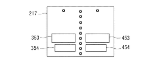
次に、図27ないし図29を参照して、本発明の第2の実施の形態に係る高周波モジュールについて説明する。図27は、本実施の形態に係る高周波モジュール1における積層基板の上面を示す平面図である。図28は、本実施の形態に係る高周波モジュール1の断面図である。なお、図28は、図27におけるB−B線の位置における断面を表わしている。図29は、本実施の形態における導体部を示す平面図である。
Claims (9)
- 交互に積層された誘電体層と導体層とを含む積層基板と、
前記積層基板の内部に設けられ、送信信号を処理する送信系回路と、
前記積層基板の内部に設けられ、受信信号を処理する受信系回路とを備えた高周波モジュールであって、
前記積層基板の内部において、前記送信系回路と受信系回路は、前記積層基板の積層方向に直交する方向に互いに分離された領域に配置され、
高周波モジュールは、更に、前記積層基板の内部において前記送信系回路が配置された領域と受信系回路が配置された領域との間に配置されると共にグランドに接続され、前記送信系回路と受信系回路とを電磁気的に分離する導体部を備え、
前記導体部は、前記送信系回路が配置された領域と受信系回路が配置された領域との間において複数の誘電体層の各々に複数個ずつ形成されたスルーホールと、それぞれ隣接する2つの誘電体層に形成された複数のスルーホールを接続するための複数のスルーホール接続用導体層とによって構成され、各誘電体層に形成された複数のスルーホールは、隣接する誘電体層に形成された複数のスルーホールと直接または前記スルーホール接続用導体層を介して接続され、
高周波モジュールは、更に、前記送信系回路と受信系回路が配置された各領域よりも前記積層基板の積層方向の一方の面に近い位置に配置されると共にグランドに接続されるグランド用導体層を備え、前記導体部は前記グランド用導体層に接続されていることを特徴とする高周波モジュール。 - 前記導体部を構成する複数のスルーホールが配置された領域は、前記積層基板の積層方向から見て線状であることを特徴とする請求項1記載の高周波モジュール。
- 前記スルーホール接続用導体層を介して接続される一方の誘電体層に形成された複数のスルーホールと他方の誘電体層に形成された複数のスルーホールは、前記積層基板の積層方向から見て、互いに異なる位置に配置されていることを特徴とする請求項1または2記載の高周波モジュール。
- 前記送信系回路と受信系回路は、アンテナに対して前記送信系回路と受信系回路のいずれかを接続するためのスイッチ回路に接続され、
前記送信系回路は、第1の周波数帯域における送信信号と前記第1の周波数帯域よりも高周波側の第2の周波数帯域における送信信号とを分離する送信系ダイプレクサであり、
前記受信系回路は、第1の周波数帯域における受信信号と前記第2の周波数帯域における受信信号とを分離する受信系ダイプレクサであることを特徴とする請求項1ないし3のいずれかに記載の高周波モジュール。 - 前記送信系ダイプレクサは、第1ないし第3のポートと、第1のポートと第2のポートとの間に設けられ、第1の周波数帯域における送信信号を通過させる第1の送信用バンドパスフィルタと、第1のポートと第3のポートとの間に設けられ、第2の周波数帯域における送信信号を通過させる第2の送信用バンドパスフィルタとを有し、第1のポートは前記スイッチ回路に接続され、
前記受信系ダイプレクサは、第1ないし第3のポートと、第1のポートと第2のポートとの間に設けられ、第1の周波数帯域における受信信号を通過させる第1の受信用バンドパスフィルタと、第1のポートと第3のポートとの間に設けられ、第2の周波数帯域における受信信号を通過させる第2の受信用バンドパスフィルタとを有し、第1のポートは前記スイッチ回路に接続されることを特徴とする請求項4記載の高周波モジュール。 - 前記各バンドパスフィルタは、共振回路を用いて構成されていることを特徴とする請求項5記載の高周波モジュール。
- 前記各共振回路は、前記導体層を用いて構成された分布定数線路を含むことを特徴とする請求項6記載の高周波モジュール。
- 前記各共振回路は、前記導体層を用いて構成されインダクタンスを有する伝送線路を含み、
前記第1の送信用バンドパスフィルタにおける共振回路に含まれる前記伝送線路の長手方向と前記第2の送信用バンドパスフィルタにおける共振回路に含まれる前記伝送線路の長手方向は直交し、
前記第1の受信用バンドパスフィルタにおける共振回路に含まれる前記伝送線路の長手方向と前記第2の受信用バンドパスフィルタにおける共振回路に含まれる前記伝送線路の長手方向は直交していることを特徴とする請求項6または7記載の高周波モジュール。 - 前記積層基板は、低温同時焼成セラミック多層基板であり、
前記積層基板には、前記送信系ダイプレクサおよび受信系ダイプレクサを構成する複数のインダクタンス素子およびキャパシタンス素子が内蔵され、
高周波モジュールは、更に、前記スイッチ回路を備え、前記スイッチ回路は、GaAs化合物半導体による電界効果トランジスタを用いて構成されて、前記積層基板に搭載され、
高周波モジュールは、更に、前記スイッチ回路をアンテナに接続するためのアンテナ端子と、前記送信系ダイプレクサを外部回路に接続するための2つの送信信号端子と、前記受信系ダイプレクサを外部回路に接続するための2つの受信信号端子と、グランドに接続されるグランド端子とを備え、前記各端子は、前記積層基板の外周面に形成されていることを特徴とする請求項4ないし8のいずれかに記載の高周波モジュール。
Priority Applications (4)
| Application Number | Priority Date | Filing Date | Title |
|---|---|---|---|
| JP2004329996A JP4134004B2 (ja) | 2004-11-15 | 2004-11-15 | 高周波モジュール |
| US11/268,653 US7565116B2 (en) | 2004-11-15 | 2005-11-08 | High frequency module |
| EP20050024604 EP1657826A3 (en) | 2004-11-15 | 2005-11-10 | High frequency module |
| CN2005101271675A CN1801645B (zh) | 2004-11-15 | 2005-11-15 | 高频模块 |
Applications Claiming Priority (1)
| Application Number | Priority Date | Filing Date | Title |
|---|---|---|---|
| JP2004329996A JP4134004B2 (ja) | 2004-11-15 | 2004-11-15 | 高周波モジュール |
Publications (2)
| Publication Number | Publication Date |
|---|---|
| JP2006140862A JP2006140862A (ja) | 2006-06-01 |
| JP4134004B2 true JP4134004B2 (ja) | 2008-08-13 |
Family
ID=35519950
Family Applications (1)
| Application Number | Title | Priority Date | Filing Date |
|---|---|---|---|
| JP2004329996A Expired - Fee Related JP4134004B2 (ja) | 2004-11-15 | 2004-11-15 | 高周波モジュール |
Country Status (4)
| Country | Link |
|---|---|
| US (1) | US7565116B2 (ja) |
| EP (1) | EP1657826A3 (ja) |
| JP (1) | JP4134004B2 (ja) |
| CN (1) | CN1801645B (ja) |
Families Citing this family (22)
| Publication number | Priority date | Publication date | Assignee | Title |
|---|---|---|---|---|
| WO2006112306A1 (ja) * | 2005-04-15 | 2006-10-26 | Hitachi Metals, Ltd. | マルチバンド高周波回路、マルチバンド高周波回路部品及びこれを用いたマルチバンド通信装置 |
| JP2007036315A (ja) | 2005-07-22 | 2007-02-08 | Tdk Corp | 高周波電子部品 |
| US9755681B2 (en) * | 2007-09-26 | 2017-09-05 | Intel Mobile Communications GmbH | Radio-frequency front-end and receiver |
| JP4923111B2 (ja) * | 2007-10-26 | 2012-04-25 | 京セラ株式会社 | ダイプレクサならびにそれを用いた無線通信モジュールおよび無線通信機器 |
| US7978031B2 (en) | 2008-01-31 | 2011-07-12 | Tdk Corporation | High frequency module provided with power amplifier |
| JP4730402B2 (ja) | 2008-06-30 | 2011-07-20 | カシオ計算機株式会社 | 撮像装置、撮像制御方法及びプログラム |
| JP4983881B2 (ja) * | 2009-09-28 | 2012-07-25 | 株式会社村田製作所 | 積層帯域通過フィルタ |
| US9236907B2 (en) | 2010-09-14 | 2016-01-12 | Hitachi Metals, Ltd. | Laminate-type electronic device with filter and balun |
| WO2012089253A1 (en) * | 2010-12-29 | 2012-07-05 | Telefonaktiebolaget Lm Ericsson (Publ) | A waveguide based five or six port circuit |
| JP5304833B2 (ja) * | 2011-04-18 | 2013-10-02 | カシオ計算機株式会社 | 撮像装置、撮像制御方法及びプログラム |
| CN103607847A (zh) * | 2013-11-20 | 2014-02-26 | 四川九洲电器集团有限责任公司 | 一种用于射频印制板的地平面与压条相结合的隔离方式 |
| CN106469689B (zh) * | 2015-08-21 | 2019-10-11 | 安世有限公司 | 电子元件及其形成方法 |
| TWI683535B (zh) | 2016-02-10 | 2020-01-21 | 日商村田製作所股份有限公司 | 雙工器 |
| JP6414559B2 (ja) | 2016-02-22 | 2018-10-31 | 株式会社村田製作所 | スイッチ付ダイプレクサモジュールおよびダイプレクサモジュール |
| TWI632769B (zh) * | 2017-04-17 | 2018-08-11 | 國立暨南國際大學 | Multiple power amplifier circuit |
| CN112470407B (zh) * | 2018-10-05 | 2022-04-26 | 株式会社村田制作所 | 高频模块以及通信装置 |
| JP2020170944A (ja) * | 2019-04-03 | 2020-10-15 | 株式会社村田製作所 | 高周波モジュール及び通信装置 |
| JP2021145282A (ja) * | 2020-03-13 | 2021-09-24 | 株式会社村田製作所 | 高周波モジュールおよび通信装置 |
| JP2021158554A (ja) * | 2020-03-27 | 2021-10-07 | 株式会社村田製作所 | 高周波モジュールおよび通信装置 |
| JP2021158556A (ja) * | 2020-03-27 | 2021-10-07 | 株式会社村田製作所 | 高周波モジュールおよび通信装置 |
| TWI793867B (zh) * | 2021-11-19 | 2023-02-21 | 啓碁科技股份有限公司 | 通訊裝置 |
| JP2024115470A (ja) * | 2023-02-14 | 2024-08-26 | Tdk株式会社 | 電子部品 |
Family Cites Families (37)
| Publication number | Priority date | Publication date | Assignee | Title |
|---|---|---|---|---|
| AU5365890A (en) | 1989-04-20 | 1990-10-25 | Nec Corporation | Miniature mobile radio communication equipment having a shield structure |
| JPH02279027A (ja) | 1989-04-20 | 1990-11-15 | Nec Corp | 無線送受信機 |
| JPH04225612A (ja) | 1990-12-27 | 1992-08-14 | Murata Mfg Co Ltd | フィルタ装置 |
| US5487184A (en) * | 1993-11-09 | 1996-01-23 | Motorola, Inc. | Offset transmission line coupler for radio frequency signal amplifiers |
| JPH07202503A (ja) | 1993-12-27 | 1995-08-04 | Murata Mfg Co Ltd | 高周波スイッチ |
| JP3694067B2 (ja) | 1995-07-19 | 2005-09-14 | Tdk株式会社 | 表面実装部品化したアンテナスイッチ |
| JPH09261110A (ja) | 1996-03-21 | 1997-10-03 | Tdk Corp | アンテナスイッチ |
| KR100233744B1 (ko) | 1995-07-19 | 1999-12-01 | 사토 히로시 | 안테나 스위치 |
| JPH09260901A (ja) | 1996-03-27 | 1997-10-03 | Hitachi Metals Ltd | スイッチ回路 |
| JPH1131905A (ja) | 1997-07-14 | 1999-02-02 | Matsushita Electric Ind Co Ltd | 分波器およびそれを用いた共用器および2周波帯域用移動体通信機器 |
| EP1909390A2 (en) | 1996-09-26 | 2008-04-09 | Matsushita Electric Industrial Co., Ltd. | Diplexer, duplexer, and two-channel mobile communications equipment |
| JP3801741B2 (ja) | 1997-08-06 | 2006-07-26 | 新日本無線株式会社 | アンテナスイッチ半導体集積回路 |
| JP2000091751A (ja) | 1998-09-10 | 2000-03-31 | Toyo Commun Equip Co Ltd | 積層基板を用いた高周波回路 |
| JP4378793B2 (ja) | 1999-06-02 | 2009-12-09 | 株式会社村田製作所 | ダイプレクサ及びそれを用いた移動体通信装置 |
| JP2001136045A (ja) | 1999-08-23 | 2001-05-18 | Murata Mfg Co Ltd | 積層型複合電子部品 |
| JP2001119209A (ja) | 1999-10-15 | 2001-04-27 | Murata Mfg Co Ltd | 積層型フィルタモジュール |
| DE60028937T2 (de) | 1999-12-14 | 2006-11-23 | Matsushita Electric Industrial Co., Ltd., Kadoma | Hochfrequenz zusammengesetzter schaltergauelement |
| JP2001185902A (ja) | 1999-12-27 | 2001-07-06 | Murata Mfg Co Ltd | 複合高周波部品及びそれを用いた通信装置 |
| WO2002017504A1 (en) * | 2000-08-22 | 2002-02-28 | Hitachi Metals, Ltd. | Laminated high-frequency switch module |
| US6759743B2 (en) | 2000-09-11 | 2004-07-06 | Xytrans, Inc. | Thick film millimeter wave transceiver module |
| JP4529262B2 (ja) * | 2000-09-14 | 2010-08-25 | ソニー株式会社 | 高周波モジュール装置及びその製造方法 |
| EP1223634A3 (en) * | 2000-12-26 | 2003-08-13 | Matsushita Electric Industrial Co., Ltd. | High-frequency switch, laminated high-frequency switch, high-frequency radio unit, and high-frequency switching method |
| US6683512B2 (en) * | 2001-06-21 | 2004-01-27 | Kyocera Corporation | High frequency module having a laminate board with a plurality of dielectric layers |
| JP2003032035A (ja) * | 2001-07-17 | 2003-01-31 | Alps Electric Co Ltd | 送受信ユニット |
| JP2003037520A (ja) | 2001-07-26 | 2003-02-07 | Murata Mfg Co Ltd | 高周波スイッチ |
| EP1418680A4 (en) | 2001-08-10 | 2005-04-06 | Hitachi Metals Ltd | DERIVATION FILTER, MUTIBAND ANTENNA SWITCHING CIRCUIT, LAMINATED MODULE COMPOSITE ELEMENT, AND COMMUNICATION DEVICE USING SAME |
| JP4006680B2 (ja) | 2001-08-31 | 2007-11-14 | 日立金属株式会社 | マルチバンドアンテナスイッチ回路およびマルチバンドアンテナスイッチ積層モジュール複合部品並びにそれを用いた通信装置 |
| DE60334888D1 (de) * | 2002-01-31 | 2010-12-23 | Hitachi Metals Ltd | Schaltnetzwerk und zusammengesetzter hochfrequenzteil |
| US6873529B2 (en) * | 2002-02-26 | 2005-03-29 | Kyocera Corporation | High frequency module |
| US6788171B2 (en) | 2002-03-05 | 2004-09-07 | Xytrans, Inc. | Millimeter wave (MMW) radio frequency transceiver module and method of forming same |
| JP2003298305A (ja) | 2002-03-28 | 2003-10-17 | Fujitsu Quantum Devices Ltd | 高周波スイッチ装置及びこれを用いた電子装置 |
| CN1327733C (zh) * | 2002-08-08 | 2007-07-18 | 松下电器产业株式会社 | 高频器件 |
| JP3790734B2 (ja) * | 2002-10-04 | 2006-06-28 | 松下電器産業株式会社 | 高周波装置、高周波増幅方法 |
| JP2004166258A (ja) | 2002-10-25 | 2004-06-10 | Hitachi Metals Ltd | 平衡−不平衡型マルチバンドフィルタモジュール |
| CN100536328C (zh) | 2002-10-25 | 2009-09-02 | 日立金属株式会社 | 平衡-不平衡型多频带滤波模块 |
| DE102004016399B4 (de) * | 2003-03-27 | 2013-06-06 | Kyocera Corp. | Hochfrequenzmodul und Funkvorrichtung |
| JP3973624B2 (ja) * | 2003-12-24 | 2007-09-12 | 富士通株式会社 | 高周波デバイス |
-
2004
- 2004-11-15 JP JP2004329996A patent/JP4134004B2/ja not_active Expired - Fee Related
-
2005
- 2005-11-08 US US11/268,653 patent/US7565116B2/en not_active Expired - Fee Related
- 2005-11-10 EP EP20050024604 patent/EP1657826A3/en not_active Ceased
- 2005-11-15 CN CN2005101271675A patent/CN1801645B/zh not_active Expired - Fee Related
Also Published As
| Publication number | Publication date |
|---|---|
| CN1801645A (zh) | 2006-07-12 |
| EP1657826A3 (en) | 2007-05-02 |
| JP2006140862A (ja) | 2006-06-01 |
| US7565116B2 (en) | 2009-07-21 |
| EP1657826A2 (en) | 2006-05-17 |
| US20060117163A1 (en) | 2006-06-01 |
| CN1801645B (zh) | 2011-06-08 |
Similar Documents
| Publication | Publication Date | Title |
|---|---|---|
| JP4134129B2 (ja) | 高周波モジュール | |
| JP2006140862A (ja) | 高周波モジュール | |
| JP5402932B2 (ja) | バンドパスフィルタ、高周波部品及び通信装置 | |
| JP5418516B2 (ja) | 分波回路、高周波回路、高周波部品、及び通信装置 | |
| JP4297368B2 (ja) | 高周波モジュール | |
| KR20120107965A (ko) | 고주파 회로, 고주파 회로 부품 및 통신 장치 | |
| JP2008193739A (ja) | 高周波モジュール | |
| US7038557B2 (en) | Antenna duplexer and mobile communication device using the same | |
| JP4134005B2 (ja) | 高周波モジュール | |
| JP2010147589A (ja) | 高周波回路、高周波部品及び通信装置 | |
| JP2008271421A (ja) | 弾性波フィルタ及び複合部品 | |
| JP2010041316A (ja) | ハイパスフィルタ、高周波モジュールおよびそれを用いた通信機器 | |
| JP2006014102A (ja) | 高周波積層モジュール部品及びこれを用いたデュアルバンド通信装置 | |
| JP4794247B2 (ja) | 高周波モジュール | |
| EP1746654A2 (en) | High frequency electronic component | |
| JP2010212962A (ja) | 高周波部品およびそれを用いた通信装置 | |
| JP4936119B2 (ja) | 積層型バラントランス及び高周波部品 | |
| JP5472672B2 (ja) | 高周波回路部品およびこれを用いた通信装置 |
Legal Events
| Date | Code | Title | Description |
|---|---|---|---|
| A977 | Report on retrieval |
Free format text: JAPANESE INTERMEDIATE CODE: A971007 Effective date: 20080128 |
|
| A131 | Notification of reasons for refusal |
Free format text: JAPANESE INTERMEDIATE CODE: A131 Effective date: 20080218 |
|
| A521 | Request for written amendment filed |
Free format text: JAPANESE INTERMEDIATE CODE: A523 Effective date: 20080417 |
|
| TRDD | Decision of grant or rejection written | ||
| A01 | Written decision to grant a patent or to grant a registration (utility model) |
Free format text: JAPANESE INTERMEDIATE CODE: A01 Effective date: 20080519 |
|
| A01 | Written decision to grant a patent or to grant a registration (utility model) |
Free format text: JAPANESE INTERMEDIATE CODE: A01 |
|
| A61 | First payment of annual fees (during grant procedure) |
Free format text: JAPANESE INTERMEDIATE CODE: A61 Effective date: 20080602 |
|
| FPAY | Renewal fee payment (event date is renewal date of database) |
Free format text: PAYMENT UNTIL: 20110606 Year of fee payment: 3 |
|
| R150 | Certificate of patent or registration of utility model |
Ref document number: 4134004 Country of ref document: JP Free format text: JAPANESE INTERMEDIATE CODE: R150 Free format text: JAPANESE INTERMEDIATE CODE: R150 |
|
| FPAY | Renewal fee payment (event date is renewal date of database) |
Free format text: PAYMENT UNTIL: 20120606 Year of fee payment: 4 |
|
| FPAY | Renewal fee payment (event date is renewal date of database) |
Free format text: PAYMENT UNTIL: 20120606 Year of fee payment: 4 |
|
| FPAY | Renewal fee payment (event date is renewal date of database) |
Free format text: PAYMENT UNTIL: 20130606 Year of fee payment: 5 |
|
| FPAY | Renewal fee payment (event date is renewal date of database) |
Free format text: PAYMENT UNTIL: 20140606 Year of fee payment: 6 |
|
| R250 | Receipt of annual fees |
Free format text: JAPANESE INTERMEDIATE CODE: R250 |
|
| S111 | Request for change of ownership or part of ownership |
Free format text: JAPANESE INTERMEDIATE CODE: R313113 |
|
| S531 | Written request for registration of change of domicile |
Free format text: JAPANESE INTERMEDIATE CODE: R313531 |
|
| R350 | Written notification of registration of transfer |
Free format text: JAPANESE INTERMEDIATE CODE: R350 |
|
| RD02 | Notification of acceptance of power of attorney |
Free format text: JAPANESE INTERMEDIATE CODE: R3D02 |
|
| R250 | Receipt of annual fees |
Free format text: JAPANESE INTERMEDIATE CODE: R250 |
|
| R250 | Receipt of annual fees |
Free format text: JAPANESE INTERMEDIATE CODE: R250 |
|
| R250 | Receipt of annual fees |
Free format text: JAPANESE INTERMEDIATE CODE: R250 |
|
| LAPS | Cancellation because of no payment of annual fees |