EP1232677B1 - Flip-chip gehäuse, schaltplatte und dessen verpackungsmethode - Google Patents
Flip-chip gehäuse, schaltplatte und dessen verpackungsmethode Download PDFInfo
- Publication number
- EP1232677B1 EP1232677B1 EP01951916A EP01951916A EP1232677B1 EP 1232677 B1 EP1232677 B1 EP 1232677B1 EP 01951916 A EP01951916 A EP 01951916A EP 01951916 A EP01951916 A EP 01951916A EP 1232677 B1 EP1232677 B1 EP 1232677B1
- Authority
- EP
- European Patent Office
- Prior art keywords
- electrodes
- circuit
- circuit board
- semiconductor element
- electrode material
- Prior art date
- Legal status (The legal status is an assumption and is not a legal conclusion. Google has not performed a legal analysis and makes no representation as to the accuracy of the status listed.)
- Expired - Lifetime
Links
Images


Classifications
-
- H—ELECTRICITY
- H10—SEMICONDUCTOR DEVICES; ELECTRIC SOLID-STATE DEVICES NOT OTHERWISE PROVIDED FOR
- H10W—GENERIC PACKAGES, INTERCONNECTIONS, CONNECTORS OR OTHER CONSTRUCTIONAL DETAILS OF DEVICES COVERED BY CLASS H10
- H10W72/00—Interconnections or connectors in packages
- H10W72/071—Connecting or disconnecting
-
- H—ELECTRICITY
- H05—ELECTRIC TECHNIQUES NOT OTHERWISE PROVIDED FOR
- H05K—PRINTED CIRCUITS; CASINGS OR CONSTRUCTIONAL DETAILS OF ELECTRIC APPARATUS; MANUFACTURE OF ASSEMBLAGES OF ELECTRICAL COMPONENTS
- H05K3/00—Apparatus or processes for manufacturing printed circuits
- H05K3/02—Apparatus or processes for manufacturing printed circuits in which the conductive material is applied to the surface of the insulating support and is thereafter removed from such areas of the surface which are not intended for current conducting or shielding
-
- H—ELECTRICITY
- H05—ELECTRIC TECHNIQUES NOT OTHERWISE PROVIDED FOR
- H05K—PRINTED CIRCUITS; CASINGS OR CONSTRUCTIONAL DETAILS OF ELECTRIC APPARATUS; MANUFACTURE OF ASSEMBLAGES OF ELECTRICAL COMPONENTS
- H05K3/00—Apparatus or processes for manufacturing printed circuits
- H05K3/30—Assembling printed circuits with electric components, e.g. with resistors
- H05K3/32—Assembling printed circuits with electric components, e.g. with resistors electrically connecting electric components or wires to printed circuits
- H05K3/321—Assembling printed circuits with electric components, e.g. with resistors electrically connecting electric components or wires to printed circuits by conductive adhesives
-
- H—ELECTRICITY
- H05—ELECTRIC TECHNIQUES NOT OTHERWISE PROVIDED FOR
- H05K—PRINTED CIRCUITS; CASINGS OR CONSTRUCTIONAL DETAILS OF ELECTRIC APPARATUS; MANUFACTURE OF ASSEMBLAGES OF ELECTRICAL COMPONENTS
- H05K1/00—Printed circuits
- H05K1/02—Details
- H05K1/09—Use of materials for the conductive, e.g. metallic pattern
- H05K1/092—Dispersed materials, e.g. conductive pastes or inks
-
- H—ELECTRICITY
- H05—ELECTRIC TECHNIQUES NOT OTHERWISE PROVIDED FOR
- H05K—PRINTED CIRCUITS; CASINGS OR CONSTRUCTIONAL DETAILS OF ELECTRIC APPARATUS; MANUFACTURE OF ASSEMBLAGES OF ELECTRICAL COMPONENTS
- H05K1/00—Printed circuits
- H05K1/02—Details
- H05K1/11—Printed elements for providing electric connections to or between printed circuits
- H05K1/111—Pads for surface mounting, e.g. lay-out
-
- H—ELECTRICITY
- H05—ELECTRIC TECHNIQUES NOT OTHERWISE PROVIDED FOR
- H05K—PRINTED CIRCUITS; CASINGS OR CONSTRUCTIONAL DETAILS OF ELECTRIC APPARATUS; MANUFACTURE OF ASSEMBLAGES OF ELECTRICAL COMPONENTS
- H05K2201/00—Indexing scheme relating to printed circuits covered by H05K1/00
- H05K2201/03—Conductive materials
- H05K2201/0332—Structure of the conductor
- H05K2201/0364—Conductor shape
- H05K2201/0367—Metallic bump or raised conductor not used as solder bump
-
- H—ELECTRICITY
- H05—ELECTRIC TECHNIQUES NOT OTHERWISE PROVIDED FOR
- H05K—PRINTED CIRCUITS; CASINGS OR CONSTRUCTIONAL DETAILS OF ELECTRIC APPARATUS; MANUFACTURE OF ASSEMBLAGES OF ELECTRICAL COMPONENTS
- H05K2201/00—Indexing scheme relating to printed circuits covered by H05K1/00
- H05K2201/09—Shape and layout
- H05K2201/09209—Shape and layout details of conductors
- H05K2201/09654—Shape and layout details of conductors covering at least two types of conductors provided for in H05K2201/09218 - H05K2201/095
- H05K2201/098—Special shape of the cross-section of conductors, e.g. very thick plated conductors
-
- H—ELECTRICITY
- H05—ELECTRIC TECHNIQUES NOT OTHERWISE PROVIDED FOR
- H05K—PRINTED CIRCUITS; CASINGS OR CONSTRUCTIONAL DETAILS OF ELECTRIC APPARATUS; MANUFACTURE OF ASSEMBLAGES OF ELECTRICAL COMPONENTS
- H05K2201/00—Indexing scheme relating to printed circuits covered by H05K1/00
- H05K2201/10—Details of components or other objects attached to or integrated in a printed circuit board
- H05K2201/10613—Details of electrical connections of non-printed components, e.g. special leads
- H05K2201/10621—Components characterised by their electrical contacts
- H05K2201/10674—Flip chip
-
- H—ELECTRICITY
- H05—ELECTRIC TECHNIQUES NOT OTHERWISE PROVIDED FOR
- H05K—PRINTED CIRCUITS; CASINGS OR CONSTRUCTIONAL DETAILS OF ELECTRIC APPARATUS; MANUFACTURE OF ASSEMBLAGES OF ELECTRICAL COMPONENTS
- H05K2203/00—Indexing scheme relating to apparatus or processes for manufacturing printed circuits covered by H05K3/00
- H05K2203/05—Patterning and lithography; Masks; Details of resist
- H05K2203/0502—Patterning and lithography
- H05K2203/0514—Photodevelopable thick film, e.g. conductive or insulating paste
-
- H—ELECTRICITY
- H10—SEMICONDUCTOR DEVICES; ELECTRIC SOLID-STATE DEVICES NOT OTHERWISE PROVIDED FOR
- H10W—GENERIC PACKAGES, INTERCONNECTIONS, CONNECTORS OR OTHER CONSTRUCTIONAL DETAILS OF DEVICES COVERED BY CLASS H10
- H10W72/00—Interconnections or connectors in packages
- H10W72/01—Manufacture or treatment
- H10W72/012—Manufacture or treatment of bump connectors, dummy bumps or thermal bumps
- H10W72/01221—Manufacture or treatment of bump connectors, dummy bumps or thermal bumps using local deposition
- H10W72/01225—Manufacture or treatment of bump connectors, dummy bumps or thermal bumps using local deposition in solid form, e.g. by using a powder or by stud bumping
-
- H—ELECTRICITY
- H10—SEMICONDUCTOR DEVICES; ELECTRIC SOLID-STATE DEVICES NOT OTHERWISE PROVIDED FOR
- H10W—GENERIC PACKAGES, INTERCONNECTIONS, CONNECTORS OR OTHER CONSTRUCTIONAL DETAILS OF DEVICES COVERED BY CLASS H10
- H10W72/00—Interconnections or connectors in packages
- H10W72/071—Connecting or disconnecting
- H10W72/073—Connecting or disconnecting of die-attach connectors
-
- H—ELECTRICITY
- H10—SEMICONDUCTOR DEVICES; ELECTRIC SOLID-STATE DEVICES NOT OTHERWISE PROVIDED FOR
- H10W—GENERIC PACKAGES, INTERCONNECTIONS, CONNECTORS OR OTHER CONSTRUCTIONAL DETAILS OF DEVICES COVERED BY CLASS H10
- H10W72/00—Interconnections or connectors in packages
- H10W72/071—Connecting or disconnecting
- H10W72/073—Connecting or disconnecting of die-attach connectors
- H10W72/07331—Connecting techniques
-
- H—ELECTRICITY
- H10—SEMICONDUCTOR DEVICES; ELECTRIC SOLID-STATE DEVICES NOT OTHERWISE PROVIDED FOR
- H10W—GENERIC PACKAGES, INTERCONNECTIONS, CONNECTORS OR OTHER CONSTRUCTIONAL DETAILS OF DEVICES COVERED BY CLASS H10
- H10W72/00—Interconnections or connectors in packages
- H10W72/071—Connecting or disconnecting
- H10W72/074—Connecting or disconnecting of anisotropic conductive adhesives
-
- H—ELECTRICITY
- H10—SEMICONDUCTOR DEVICES; ELECTRIC SOLID-STATE DEVICES NOT OTHERWISE PROVIDED FOR
- H10W—GENERIC PACKAGES, INTERCONNECTIONS, CONNECTORS OR OTHER CONSTRUCTIONAL DETAILS OF DEVICES COVERED BY CLASS H10
- H10W72/00—Interconnections or connectors in packages
- H10W72/20—Bump connectors, e.g. solder bumps or copper pillars; Dummy bumps; Thermal bumps
- H10W72/231—Shapes
- H10W72/234—Cross-sectional shape, i.e. in side view
-
- H—ELECTRICITY
- H10—SEMICONDUCTOR DEVICES; ELECTRIC SOLID-STATE DEVICES NOT OTHERWISE PROVIDED FOR
- H10W—GENERIC PACKAGES, INTERCONNECTIONS, CONNECTORS OR OTHER CONSTRUCTIONAL DETAILS OF DEVICES COVERED BY CLASS H10
- H10W72/00—Interconnections or connectors in packages
- H10W72/20—Bump connectors, e.g. solder bumps or copper pillars; Dummy bumps; Thermal bumps
- H10W72/251—Materials
-
- H—ELECTRICITY
- H10—SEMICONDUCTOR DEVICES; ELECTRIC SOLID-STATE DEVICES NOT OTHERWISE PROVIDED FOR
- H10W—GENERIC PACKAGES, INTERCONNECTIONS, CONNECTORS OR OTHER CONSTRUCTIONAL DETAILS OF DEVICES COVERED BY CLASS H10
- H10W72/00—Interconnections or connectors in packages
- H10W72/20—Bump connectors, e.g. solder bumps or copper pillars; Dummy bumps; Thermal bumps
- H10W72/251—Materials
- H10W72/252—Materials comprising solid metals or solid metalloids, e.g. PbSn, Ag or Cu
-
- H—ELECTRICITY
- H10—SEMICONDUCTOR DEVICES; ELECTRIC SOLID-STATE DEVICES NOT OTHERWISE PROVIDED FOR
- H10W—GENERIC PACKAGES, INTERCONNECTIONS, CONNECTORS OR OTHER CONSTRUCTIONAL DETAILS OF DEVICES COVERED BY CLASS H10
- H10W72/00—Interconnections or connectors in packages
- H10W72/20—Bump connectors, e.g. solder bumps or copper pillars; Dummy bumps; Thermal bumps
- H10W72/261—Functions other than electrical connecting
-
- H—ELECTRICITY
- H10—SEMICONDUCTOR DEVICES; ELECTRIC SOLID-STATE DEVICES NOT OTHERWISE PROVIDED FOR
- H10W—GENERIC PACKAGES, INTERCONNECTIONS, CONNECTORS OR OTHER CONSTRUCTIONAL DETAILS OF DEVICES COVERED BY CLASS H10
- H10W72/00—Interconnections or connectors in packages
- H10W72/30—Die-attach connectors
- H10W72/321—Structures or relative sizes of die-attach connectors
- H10W72/325—Die-attach connectors having a filler embedded in a matrix
-
- H—ELECTRICITY
- H10—SEMICONDUCTOR DEVICES; ELECTRIC SOLID-STATE DEVICES NOT OTHERWISE PROVIDED FOR
- H10W—GENERIC PACKAGES, INTERCONNECTIONS, CONNECTORS OR OTHER CONSTRUCTIONAL DETAILS OF DEVICES COVERED BY CLASS H10
- H10W72/00—Interconnections or connectors in packages
- H10W72/30—Die-attach connectors
- H10W72/351—Materials of die-attach connectors
- H10W72/352—Materials of die-attach connectors comprising metals or metalloids, e.g. solders
-
- H—ELECTRICITY
- H10—SEMICONDUCTOR DEVICES; ELECTRIC SOLID-STATE DEVICES NOT OTHERWISE PROVIDED FOR
- H10W—GENERIC PACKAGES, INTERCONNECTIONS, CONNECTORS OR OTHER CONSTRUCTIONAL DETAILS OF DEVICES COVERED BY CLASS H10
- H10W72/00—Interconnections or connectors in packages
- H10W72/30—Die-attach connectors
- H10W72/351—Materials of die-attach connectors
- H10W72/353—Materials of die-attach connectors not comprising solid metals or solid metalloids, e.g. ceramics
- H10W72/354—Materials of die-attach connectors not comprising solid metals or solid metalloids, e.g. ceramics comprising polymers
-
- H—ELECTRICITY
- H10—SEMICONDUCTOR DEVICES; ELECTRIC SOLID-STATE DEVICES NOT OTHERWISE PROVIDED FOR
- H10W—GENERIC PACKAGES, INTERCONNECTIONS, CONNECTORS OR OTHER CONSTRUCTIONAL DETAILS OF DEVICES COVERED BY CLASS H10
- H10W72/00—Interconnections or connectors in packages
- H10W72/50—Bond wires
- H10W72/551—Materials of bond wires
- H10W72/552—Materials of bond wires comprising metals or metalloids, e.g. silver
- H10W72/5522—Materials of bond wires comprising metals or metalloids, e.g. silver comprising gold [Au]
-
- H—ELECTRICITY
- H10—SEMICONDUCTOR DEVICES; ELECTRIC SOLID-STATE DEVICES NOT OTHERWISE PROVIDED FOR
- H10W—GENERIC PACKAGES, INTERCONNECTIONS, CONNECTORS OR OTHER CONSTRUCTIONAL DETAILS OF DEVICES COVERED BY CLASS H10
- H10W72/00—Interconnections or connectors in packages
- H10W72/90—Bond pads, in general
-
- H—ELECTRICITY
- H10—SEMICONDUCTOR DEVICES; ELECTRIC SOLID-STATE DEVICES NOT OTHERWISE PROVIDED FOR
- H10W—GENERIC PACKAGES, INTERCONNECTIONS, CONNECTORS OR OTHER CONSTRUCTIONAL DETAILS OF DEVICES COVERED BY CLASS H10
- H10W72/00—Interconnections or connectors in packages
- H10W72/90—Bond pads, in general
- H10W72/941—Dispositions of bond pads
- H10W72/9415—Dispositions of bond pads relative to the surface, e.g. recessed, protruding
-
- H—ELECTRICITY
- H10—SEMICONDUCTOR DEVICES; ELECTRIC SOLID-STATE DEVICES NOT OTHERWISE PROVIDED FOR
- H10W—GENERIC PACKAGES, INTERCONNECTIONS, CONNECTORS OR OTHER CONSTRUCTIONAL DETAILS OF DEVICES COVERED BY CLASS H10
- H10W90/00—Package configurations
- H10W90/701—Package configurations characterised by the relative positions of pads or connectors relative to package parts
- H10W90/721—Package configurations characterised by the relative positions of pads or connectors relative to package parts of bump connectors
- H10W90/724—Package configurations characterised by the relative positions of pads or connectors relative to package parts of bump connectors between a chip and a stacked insulating package substrate, interposer or RDL
Definitions
- the present invention relates to a flip chip package, a circuit board thereof and a packaging method thereof, and specifically to a flip chip package having an electrode structure suitable for a flip chip package, a circuit board thereof and a packaging method thereof.
- SBB method Stamped Bump Bonding
- the SBB method is a technique for forming protruding electrodes, which are made of materials such as Au, on a semiconductor element by a wire bonding method and for connecting the protruding electrodes and electrodes on a circuit board via conductive resin.
- a paste electrode material is firstly printed on a circuit board 11 by a method such as screen printing, and the circuit board 11 is baked at a temperature of sintering the electrode material.
- circuit electrodes 12 are formed on the circuit board 11.
- protruding electrodes 14 are formed on a semiconductor element 13 by a method such as wire bonding, and a layer of conductive resin 15 is formed on the protruding electrodes 14 by transferring and so on.
- the circuit board 11 and the semiconductor element 13 are positioned high accurately and a suitable load is applied thereon.
- the semiconductor element 13 is packaged on the circuit board 11.
- the above conventional packaging method is disadvantageous as in the following.
- a pitch is limited up to 300 ⁇ m and printing is difficult with a pitch below the limit, causing frequent short circuits and breaks in a wire. Consequently, the yields are lowered.
- a quantity of the conductive resin 15 is set smaller than that of the conventional art.
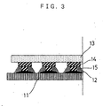
- the circuit electrodes 12 are each half-round in cross section when an electrode pitch is 100 ⁇ m.
- the conductive resin 15 is squeezed out of the circuit electrodes 12 as shown in FIG. 3 . Therefore, the conductive resin 15, which is squeezed out of the adjacent circuit electrodes 12, may be short-circuited.
- EP 0 657 932 discloses a chip carrier with a plurality of electrodes on the carrier body for mounting a chip in a flip-chip fashion, thereby forming a connection between the electrodes of the chip and those of the chip carrier with a conductive adhesive to improve the connection, wherein spreading of the conductive adhesive is prevented by forming the electrodes in a two-step shape with a narrower part at the tip end.
- JP 08 222 840 discloses a method to form a circuit board with an electrode pad, wherein a pattern of electrodes with a concave surface is formed with conductor paste, the dried electrode bodies are baked and electrode pads are formed thereof by electroless plating. Spreading of the conductor paste is prevented by the concave shape of the pads.
- the object of the present invention is to make a stable connection with a circuit board even when a semiconductor element has a small electrode pitch.
- the method of the present invention comprises the steps :
- concave circuit electrodes having warped edges are formed on the circuit board. Since the concave surfaces of the circuit electrodes act as saucers, it is possible to flip-chip package the semiconductor element without squeezing out any conductive resin. Consequently, it is possible to eliminate the occurrence of short circuits, achieving a reliable packaging for the semiconductor element.
- the circuit board can be provided not only with a circuit including circuit electrodes for mounting the above semiconductor element, but also a circuit for mounting components other than the semiconductor element as well as a circuit for making connection with another board.
- Such an electrode material contains, at least, metallic materials such as Au, Ag, or Cu and glass as inorganic components, and a monomer and a polymer which also serve as polymeric materials and a photoinitiator as organic components. Ni or Au plating may be applied to the surface of the formed circuit electrodes.
- Such a semiconductor element is used that is formed with the protruding electrodes made of metallic materials such as Au, A1, Cu, and solder. Any method including wire bonding and plating is applicable for forming the protruding electrodes.
- the conductive resin is applicable as long as the resin contains conductive components such as Au, Ag, and Cu to connect the protruding electrodes on the semiconductor element and the circuit electrodes on the circuit board. Any type of resin is applicable regardless of whether it is thermosetting or thermoplastic.
- a film is formed by printing a paste electrode material on the circuit board.
- the electrode material needs to be printed only on a package region for packaging the semiconductor element.
- the other regions may be formed with a circuit pattern in advance according to the above mentioned conventional method.
- printing may be performed over the entire surface of the package region.
- a rough printing such as a conventional screen printing is sufficiently applicable.
- the electrode material is dried at a suitable temperature to prevent the material from flowing after printing.
- a printing plate and printing conditions need be set so as to secure a prescribed film thickness, which is preferably 10 to 20 ( ⁇ m).
- step (b) a glass mask and so on are positioned on the circuit board, on which the electrode material is printed and dried.
- the glass mask is formed such that only an electrode region having the semiconductor element transmits light.
- Ultraviolet rays having a wavelength of 320 to 370 nm are radiated at 300 to 500 mJ.
- polymeric materials on an electrode region which transmits ultraviolet rays are started by a photoinitiator to react and polymerized.
- the board is entirely developed by means of a solution for dissolving the polymeric material which has not reacted.
- the film is removed from other parts than the electrode regions and remains on the electrode regions.
- step (c) the circuit board completed with exposure and development is baked at a temperature for sintering the electrode material, and the circuit electrodes are baked onto the circuit board.
- the electrode material film is caused to slightly shrink, so that both ends of the formed circuit electrode are slightly warped (such warped part is called an edge curl) and the cross section of the circuit electrode becomes arc-shaped.
- Plating of Ni, Au and so on may be applied in order to protect the electrode surfaces after baking.
- step (d) the semiconductor element having the protruding electrodes formed thereon is flip-chip packaged on the circuit board by using the conductive resin.
- the edge curl of the circuit electrode acts as a wall, thereby preventing the conductive resin from being squeezed out.
- a semiconductor element when a semiconductor element is flip-chip packaged on a circuit board by using a conductive resin, the element having protruding electrodes formed thereon, an electrode material containing photopolymerizable materials is printed on a semiconductor element package region on the circuit board such that a film is formed with a prescribed thickness, concave circuit electrodes are formed by baking the electrode material film after exposure and development are performed so as to allow the electrode material film to remain only on prescribed electrode regions, the concave circuit electrode having edges warped in a direction of going apart from a board surface, the protruding electrodes formed on the semiconductor element are brought into contact with the concave sides of the concave circuit electrodes, and the protruding electrodes and the circuit electrodes are connected with each other via the conductive resin.
- the electrode material film is formed with a dry film thickness of 10 to 20 micrometers by using a flip-chip packaging method.
- the electrode material film remaining after development is trapezoidal in cross section that is wider as it goes farther from the circuit board.
- circuit electrode is arc-shaped in cross section.
- the present invention also relates to a flip-chip package, in which the semiconductor element having the protruding electrodes formed thereon is packaged on the circuit board by using the conductive resin, wherein the circuit board includes the concave circuit electrodes each having edges warped in a direction of going apart from the board surface, the semiconductor element is disposed such that the ends of the protruding electrodes are in contact with the concave surfaces of the concave circuit electrodes, and the protruding electrodes and the circuit electrodes are connected to each other via the conductive resin.
- the circuit board for flip-chip packaging the semiconductor element by using the conductive resin, the semiconductor element having protruding electrodes formed thereon includes concave circuit electrodes, each having edges warped in a direction of going apart from the board surface.
- FIG. 1 is a process sectional view explaining a method of packaging a semiconductor element according to Embodiment 1 of the present invention.
- a paste electrode material 2 containing photopolymerizable materials is printed on an area for placing a semiconductor element on a circuit board 1. After printing, the electrode material 2 is dried at a suitable temperature without flowing. At this moment, the electrode material 2 is printed while a printing type and conditions are determined so as to have a film thickness of 10 to 20 ⁇ m after drying.
- a glass mask 3 is disposed on the film of the electrode material 2 while being positioned on the circuit board 1. Openings 3a are formed on the glass mask 3 to transmit light through a desired circuit pattern. To be specific, the 50 ⁇ m-width openings 3a corresponding to electrode regions are formed with a 100 ⁇ m-pitch. Then, UV (ultraviolet ray) having a wavelength of 320 to 370 nm is radiated at 300 to 500 mJ from the above of the glass mask 3.
- UV ultraviolet
- photopolymerizable materials of the electrode material 2 on the electrode regions 2a i.e., a photoinitiator, a monomer, and a polymer are reacted with one another to proceed polymerization.
- photopolymerizable materials of the electrode material 2 on non-electrode regions 2b polymerization does not occur. Since UV is not likely to enter the neighborhood of the circuit board 1, the electrode materials 2 are not likely to be polymerized on these regions.
- the electrode material 2 is developed by using an alkaline solution and so on.
- this operation removes the electrode material 2 on the non-electrode regions 2b.
- polymerization is proceeded completely.
- the electrode material 2 remains without any erosion so as to correspond in shape to the openings 3a of the glass mask 3.
- the electrode material 2 around the circuit board 1 polymerization is not completed over a wide region as compared with the neighborhood of the surface, resulting in erosion larger than the openings 3a. Consequently, the electrode material 2 on the electrode region 2a is trapezoidal in cross section.
- the electrode material 2 on the circuit board 1 is baked as circuit electrodes 4.
- the electrode material 2 contracts upon baking, the edges of the circuit electrodes 4 are warped in a direction of going apart from the circuit board 1 (edge cur1), and the circuit electrodes 4 are arc-shaped depressions in cross section.
- the semiconductor element 7, on which conductive resin 6 is transferred to protruding electrodes 5, is accurately positioned to the circuit substrate 1 such that the protruding electrodes 5 and the circuit electrodes 4 are opposed to each other.
- a suitable load is applied to the semiconductor element 7, the protruding electrodes 5 and the circuit electrodes 4 are brought into contact with each other, and the conductive.resin 6 is cured.
- the flip chip packaging of the semiconductor element 7 is completed.
- the edge-curled circuit electrodes 4 prevent the conductive resin 6 from being squeezed out of the circuit electrodes 4. Therefore, at the time of packaging the semiconductor element 7 with a 100- ⁇ m electrode pitch, the conductive resin 6 expanding laterally does not cause any short circuits between the adjacent electrodes.
- circuit electrodes 4 will be further discussed.
- an edge curl amount L a maximum distance from the surface of the circuit board 1 to the edge-curled circuit electrodes 4 is defined as an edge curl amount L (see FIG. 1(e) ).
- An edge curl amount L is considerably dependent upon a dry film thickness of the electrode material 2 shown in FIG. 1(a) . When a dry film thickness is 10 to 20 ⁇ m, an edge curl amount L is 2 to 10 ⁇ m.
- the circuit electrodes 4 can act as saucers.
- FIG. 2 is a process sectional view explaining a method of packaging a semiconductor element according to Embodiment 2 of the present invention.
- edge-curled circuit electrodes 4 are formed on a circuit substrate 1. And then a mask (not shown) having openings corresponding to the circuit electrodes 4 is positioned onto the circuit electrodes 4, and conductive resin 6 is applied to the circuit electrodes 4 as shown in FIG. 2(b) by using a printing method and so on. Thereafter, as shown in FIG. 2(c) , a semiconductor element 7 having protruding electrodes 5 formed thereon is positioned to the circuit board 1, and a suitable load is applied onto the semiconductor element 7. Hence, the flip chip packaging of the semiconductor element 7 is completed.
- the edge-curled circuit electrodes 4 act as saucers to prevent the conductive resin 6 from being squeezed out, thereby eliminating the occurrence of short circuits.
- a semiconductor element is packaged according to the above manufacturing steps and the performance is evaluated. Used members and materials are:
- the electrode material 2 contains Ag as a metallic component with a dry film thickness of about 15 ⁇ m. And then, the electrode material film is exposed and developed using a glass mask having openings formed thereon. The openings are each about 50 ⁇ m in width.
- the electrode material 2 on the non-electrode regions 2b having no or insufficient polymerization is dissolved and removed.
- the circuit board 1, on which the electrode material 2 on the non-electrode regions 2b is dissolved and removed, is baked at about 800 to 1000°C. Hence, the electrode material 2 on the circuit board 1 is baked as circuit electrodes 4. At this moment, an edge curl amount L is 4 ⁇ m. Ni plating and Au plating are applied to protect the surface.
- the protruding electrodes 5 are formed on the electrodes of the above IC by using metallic wires, and the conductive resin 6 is transferred onto the formed protruding electrodes 5.
- the conductive resin 6 contains Ag as a metallic component and epoxy as a resin component.
- the IC including the conductive resin 6 is positioned onto the circuit board 1 and a weight of several grams is applied to each of the protruding electrodes so as to complete packaging. And then, after curing the conductive resin 6 by heating, evaluation is made on short/open.
- FIG. 1 shows the result. Table 1 Method of Present Invention Open 0/5 Package Short 0/5 Package Conventional Method Open 0/5 Package Short 4/5 Package
- the method of the present invention does not cause any opens or short circuits at all. Meanwhile, the conventional method causes short circuits on a 4/5 package. Thus, the effectiveness of the present invention can be confirmed.
- the edge-curled circuit electrodes are formed on the circuit board, and the protruding electrodes of the semiconductor element are connected to the circuit electrodes by using the conductive resin.
- the conductive resin it is possible to prevent the conductive resin from being squeezed out while the circuit electrodes act as saucers, achieving a reliable packaging for the semiconductor element without any occurrence of short circuits.
Landscapes
- Engineering & Computer Science (AREA)
- Manufacturing & Machinery (AREA)
- Microelectronics & Electronic Packaging (AREA)
- Wire Bonding (AREA)
- Encapsulation Of And Coatings For Semiconductor Or Solid State Devices (AREA)
- Electric Connection Of Electric Components To Printed Circuits (AREA)
- Structures For Mounting Electric Components On Printed Circuit Boards (AREA)
- Manufacturing Of Printed Wiring (AREA)
- Auxiliary Devices For And Details Of Packaging Control (AREA)
Claims (6)
- Flip-Chip-Montageverfahren für Flip-Chip-Montage eines Halbleiterelementes (7), an dem vorstehende Elektroden (5) ausgebildet sind, auf einer Leiterplatte (1) unter Verwendung eines leitenden Harzes (6), wobei das Verfahren die folgenden Schritte umfasst:Drucken eines Elektrodenmaterials (2), das fotopolymerisierbare Materialien enthält, auf einen Halbleiterelement-Montagebereich auf der Leiterplatte (1), so dass ein Film mit einer vorgeschriebenen Dicke ausgebildet wird, und Ausbilden konkaver Schaltungselektroden (4) durch Brennen des Films (2) aus Elektrodenmaterial nach Durchführen von Belichtung und Entwicklung des Films (2) aus Elektrodenmaterial, so dass der Film (2) aus Elektrodenmaterial nur auf vorgeschriebenen Elektrodenbereichen (2a) verbleiben kann, um so konkave Schaltungselektroden (4) auszubilden, die Ränder haben, die in einer Richtung von der Leiterplatten-Oberfläche (1) weg gekrümmt sind; undAnlegen der vorstehenden Elektroden (5), die an dem Halbleiterelement (7) ausgebildet sind, an konkave Flächen der konkaven Schaltungselektroden (4) sowie Verbinden der vorstehenden Elektroden (5) und der Schaltungselektroden (4) miteinander über das leitende Harz (6).
- Flip-Chip-Montageverfahren nach Anspruch 1, wobei der Film (2) aus Elektrodenmaterial so ausgebildet wird, dass er eine Trockenfilmdicke von 10 bis 20 µm hat.
- Flip-Chip-Montageverfahren nach Anspruch 1 oder 2, wobei der Film (2a) aus Elektrodenmaterial, der nach Entwicklung zurückbleibt, im Querschnitt Trapezform hat, die mit zunehmender Entfernung von der Leiterplatte (1) breiter wird.
- Flip-Chip-Montageverfahren nach Anspruch 1 oder 2, wobei die Schaltungselektrode (4) im Querschnitt bogenförmig ist.
- Flip-Chip-Baugruppe, bei der ein Halbleiterelement (7), an dem vorstehende Elektroden (5) ausgebildet sind, unter Verwendung eines leitenden Harzes (6) an einer Leiterplatte (1) montiert ist, wobeidie Leiterplatte (1) Schaltungselektroden (4) enthält,das Halbleiterelement (7) so angeordnet ist, dass Enden der vorstehenden Elektroden (5) an Flächen der Schaltungselektroden (4) anliegen, unddie vorstehenden Elektroden (5) und die Schaltungselektroden (4) über das leitende Harz (6) miteinander verbunden sind,
dadurch gekennzeichnet, dassdie Schaltungselektroden (4) konkav sind und jeweils Ränder haben, die in einer Richtung von der Leiterplatten-Oberfläche (1) weg gekrümmt sind, und die vorstehenden Elektroden (5) an den konkaven Flächen der konkaven Schaltungselektroden (4) anliegen. - Leiterplatte für Flip-Chip-Montage eines Halbleiterelementes (7) unter Verwendung eines leitenden Harzes (6), wobei an dem Halbleiterelement (7) vorstehende Elektroden (5) ausgebildet ist, und die Leiterplatte umfasst:Schaltungselektroden (4),
dadurch gekennzeichnet, dassdie Schaltungselektroden konkav sind und jeweils Ränder haben, die in einer Richtung von der Leiterplatten-Oberfläche (1) weg gekrümmt sind.
Applications Claiming Priority (3)
| Application Number | Priority Date | Filing Date | Title |
|---|---|---|---|
| JP2000219911A JP3549017B2 (ja) | 2000-07-21 | 2000-07-21 | フリップチップ実装方法 |
| JP2000219911 | 2000-07-21 | ||
| PCT/JP2001/006230 WO2002009485A2 (en) | 2000-07-21 | 2001-07-18 | Flip chip package, circuit board thereof and packaging method thereof |
Publications (2)
| Publication Number | Publication Date |
|---|---|
| EP1232677A2 EP1232677A2 (de) | 2002-08-21 |
| EP1232677B1 true EP1232677B1 (de) | 2009-09-09 |
Family
ID=18714606
Family Applications (1)
| Application Number | Title | Priority Date | Filing Date |
|---|---|---|---|
| EP01951916A Expired - Lifetime EP1232677B1 (de) | 2000-07-21 | 2001-07-18 | Flip-chip gehäuse, schaltplatte und dessen verpackungsmethode |
Country Status (9)
| Country | Link |
|---|---|
| US (2) | US6750132B2 (de) |
| EP (1) | EP1232677B1 (de) |
| JP (1) | JP3549017B2 (de) |
| KR (1) | KR100429740B1 (de) |
| CN (1) | CN1239056C (de) |
| AT (1) | ATE442764T1 (de) |
| DE (1) | DE60139852D1 (de) |
| TW (1) | TW517317B (de) |
| WO (1) | WO2002009485A2 (de) |
Families Citing this family (11)
| Publication number | Priority date | Publication date | Assignee | Title |
|---|---|---|---|---|
| JP4639586B2 (ja) * | 2003-12-05 | 2011-02-23 | セイコーエプソン株式会社 | 導電パターンの形成方法、配線の形成方法、半導体装置の製造方法、回路基板の製造方法、並びに、電子部品の製造方法 |
| US20070045647A1 (en) * | 2005-09-01 | 2007-03-01 | Wintek Corporation | Display panel package |
| CN101432861B (zh) * | 2006-04-27 | 2011-02-09 | 松下电器产业株式会社 | 连接构造体及其制造方法 |
| AT505111B1 (de) * | 2007-04-12 | 2009-05-15 | Rosenbauer Int Ag | Einsatzvorrichtung zur brandbekämpfung |
| KR100842921B1 (ko) | 2007-06-18 | 2008-07-02 | 주식회사 하이닉스반도체 | 반도체 패키지의 제조 방법 |
| JP5104687B2 (ja) | 2008-09-19 | 2012-12-19 | 日本電気株式会社 | 接合シート及び電子回路装置並びに製造方法 |
| JP5002633B2 (ja) * | 2009-09-30 | 2012-08-15 | 三洋電機株式会社 | 半導体モジュールおよび携帯機器 |
| CN101807532B (zh) * | 2010-03-30 | 2012-05-09 | 上海凯虹科技电子有限公司 | 一种超薄芯片的倒装式封装方法以及封装体 |
| KR102082778B1 (ko) | 2012-08-27 | 2020-03-02 | 삼성디스플레이 주식회사 | Fpcb 조립체 및 그것을 채용한 평판 표시 장치 |
| KR101431918B1 (ko) * | 2012-12-31 | 2014-08-19 | 삼성전기주식회사 | 인쇄회로기판 및 인쇄회로기판의 표면처리방법 |
| CN112822866B (zh) * | 2021-01-07 | 2022-05-27 | Tcl华星光电技术有限公司 | 用于表面贴装的锡膏、驱动电路板及表面贴装方法 |
Family Cites Families (14)
| Publication number | Priority date | Publication date | Assignee | Title |
|---|---|---|---|---|
| US5049480A (en) * | 1990-02-20 | 1991-09-17 | E. I. Du Pont De Nemours And Company | Photosensitive aqueous developable silver conductor composition |
| JPH0666355A (ja) | 1992-08-20 | 1994-03-08 | Mitsubishi Motors Corp | 自動車のエンジンとトルクコンバータとの結合構造 |
| US5338391A (en) | 1993-10-12 | 1994-08-16 | Motorola, Inc. | Method of making a substrate having selectively releasing conductive runners |
| US5640051A (en) * | 1993-12-13 | 1997-06-17 | Matsushita Electric Industrial Co., Ltd. | Chip package, a chip carrier, a terminal electrode for a circuit substrate and a chip package-mounted complex |
| JP3320932B2 (ja) * | 1993-12-13 | 2002-09-03 | 松下電器産業株式会社 | チップパッケージ実装体、及びチップパッケージが実装される回路基板、並びに回路基板の形成方法 |
| US5508228A (en) * | 1994-02-14 | 1996-04-16 | Microelectronics And Computer Technology Corporation | Compliant electrically connective bumps for an adhesive flip chip integrated circuit device and methods for forming same |
| JPH0878476A (ja) * | 1994-09-08 | 1996-03-22 | Hitachi Ltd | 半導体集積回路装置 |
| JPH08222840A (ja) * | 1995-02-15 | 1996-08-30 | Sumitomo Metal Ind Ltd | 電極パッド付き回路基板およびその製造方法 |
| US5903056A (en) * | 1997-04-21 | 1999-05-11 | Lucent Technologies Inc. | Conductive polymer film bonding technique |
| JP3070514B2 (ja) * | 1997-04-28 | 2000-07-31 | 日本電気株式会社 | 突起電極を有する半導体装置、半導体装置の実装方法およびその実装構造 |
| JPH11121527A (ja) * | 1997-10-21 | 1999-04-30 | Pfu Ltd | ベアチップ実装方法およびセラミック基板の製造方法およびセラミック基板ならびに半導体装置 |
| US6078100A (en) * | 1999-01-13 | 2000-06-20 | Micron Technology, Inc. | Utilization of die repattern layers for die internal connections |
| JP4159213B2 (ja) * | 1999-11-17 | 2008-10-01 | 日本アビオニクス株式会社 | フリップチップ実装方法 |
| JP2001267366A (ja) * | 2000-03-16 | 2001-09-28 | Matsushita Electric Ind Co Ltd | 半導体実装方法およびプリント回路基板 |
-
2000
- 2000-07-21 JP JP2000219911A patent/JP3549017B2/ja not_active Expired - Fee Related
-
2001
- 2001-07-18 AT AT01951916T patent/ATE442764T1/de active
- 2001-07-18 US US10/088,479 patent/US6750132B2/en not_active Expired - Lifetime
- 2001-07-18 CN CNB018021085A patent/CN1239056C/zh not_active Expired - Fee Related
- 2001-07-18 DE DE60139852T patent/DE60139852D1/de not_active Expired - Lifetime
- 2001-07-18 WO PCT/JP2001/006230 patent/WO2002009485A2/en not_active Ceased
- 2001-07-18 EP EP01951916A patent/EP1232677B1/de not_active Expired - Lifetime
- 2001-07-18 KR KR10-2002-7003675A patent/KR100429740B1/ko not_active Expired - Fee Related
- 2001-07-19 TW TW090117657A patent/TW517317B/zh not_active IP Right Cessation
-
2004
- 2004-05-06 US US10/839,157 patent/US7034389B2/en not_active Expired - Fee Related
Also Published As
| Publication number | Publication date |
|---|---|
| TW517317B (en) | 2003-01-11 |
| US7034389B2 (en) | 2006-04-25 |
| DE60139852D1 (de) | 2009-10-22 |
| CN1386394A (zh) | 2002-12-18 |
| US20020175407A1 (en) | 2002-11-28 |
| KR20020030122A (ko) | 2002-04-22 |
| EP1232677A2 (de) | 2002-08-21 |
| US6750132B2 (en) | 2004-06-15 |
| CN1239056C (zh) | 2006-01-25 |
| JP2002043364A (ja) | 2002-02-08 |
| WO2002009485A2 (en) | 2002-01-31 |
| JP3549017B2 (ja) | 2004-08-04 |
| ATE442764T1 (de) | 2009-09-15 |
| US20040227253A1 (en) | 2004-11-18 |
| KR100429740B1 (ko) | 2004-05-03 |
| WO2002009485A3 (en) | 2002-06-06 |
Similar Documents
| Publication | Publication Date | Title |
|---|---|---|
| US7674362B2 (en) | Method for fabrication of a conductive bump structure of a circuit board | |
| US5783465A (en) | Compliant bump technology | |
| CN101064270B (zh) | 半导体器件的制造方法 | |
| US7579684B2 (en) | Methods for packing microfeature devices and microfeature devices formed by such methods | |
| KR100597993B1 (ko) | 반도체 패키지용 범프, 그 범프를 적용한 반도체 패키지 및 제조방법 | |
| JP3108716B2 (ja) | 半導体チップスケール半導体パッケージ及びその製造方法 | |
| EP1096567A2 (de) | KMG und seine Herstellung | |
| US6338985B1 (en) | Making chip size semiconductor packages | |
| JP3450236B2 (ja) | 半導体装置及びその製造方法 | |
| US6750132B2 (en) | Flip chip package, circuit board thereof and packaging method thereof | |
| US7151050B2 (en) | Method for fabricating electrical connection structure of circuit board | |
| US6946601B1 (en) | Electronic package with passive components | |
| US7341934B2 (en) | Method for fabricating conductive bump of circuit board | |
| JPH10233463A (ja) | 半導体装置およびその製造方法 | |
| JP4015787B2 (ja) | 半導体装置の製造方法 | |
| JP2001135662A (ja) | 半導体素子および半導体装置の製造方法 | |
| JP3926335B2 (ja) | フリップチップ実装体およびそのための回路基板 | |
| WO2003013201A1 (en) | Method for forming device-landing pad of multi-layered printed circuit board | |
| JP3115807B2 (ja) | 半導体装置 | |
| KR100341530B1 (ko) | 볼 그리드 어레이 타입 인쇄회로기판의 솔더볼 패드형성방법 | |
| JP2002299361A (ja) | 半導体装置及びその製造方法、回路基板並びに電子機器 | |
| KR20050009035A (ko) | 일회용 마스크를 이용한 솔더 볼 형성 방법 | |
| JPH09266369A (ja) | プリント基板の加工方法並びにプリント基板 | |
| CN115692207A (zh) | 封装基板及其制作方法 | |
| KR19990005676A (ko) | 패키지용 기판의 비어홀내 잉크 충진방법 |
Legal Events
| Date | Code | Title | Description |
|---|---|---|---|
| PUAI | Public reference made under article 153(3) epc to a published international application that has entered the european phase |
Free format text: ORIGINAL CODE: 0009012 |
|
| 17P | Request for examination filed |
Effective date: 20020410 |
|
| AK | Designated contracting states |
Kind code of ref document: A2 Designated state(s): AT BE CH CY DE DK ES FI FR GB GR IE IT LI LU MC NL PT SE TR |
|
| RBV | Designated contracting states (corrected) |
Designated state(s): AT BE CH CY DE FR GB LI |
|
| 17Q | First examination report despatched |
Effective date: 20070122 |
|
| RAP1 | Party data changed (applicant data changed or rights of an application transferred) |
Owner name: PANASONIC CORPORATION |
|
| GRAP | Despatch of communication of intention to grant a patent |
Free format text: ORIGINAL CODE: EPIDOSNIGR1 |
|
| RBV | Designated contracting states (corrected) |
Designated state(s): AT DE FR GB |
|
| GRAS | Grant fee paid |
Free format text: ORIGINAL CODE: EPIDOSNIGR3 |
|
| GRAA | (expected) grant |
Free format text: ORIGINAL CODE: 0009210 |
|
| AK | Designated contracting states |
Kind code of ref document: B1 Designated state(s): AT DE FR GB |
|
| REG | Reference to a national code |
Ref country code: GB Ref legal event code: FG4D |
|
| REF | Corresponds to: |
Ref document number: 60139852 Country of ref document: DE Date of ref document: 20091022 Kind code of ref document: P |
|
| PLBE | No opposition filed within time limit |
Free format text: ORIGINAL CODE: 0009261 |
|
| STAA | Information on the status of an ep patent application or granted ep patent |
Free format text: STATUS: NO OPPOSITION FILED WITHIN TIME LIMIT |
|
| 26N | No opposition filed |
Effective date: 20100610 |
|
| PGFP | Annual fee paid to national office [announced via postgrant information from national office to epo] |
Ref country code: GB Payment date: 20120718 Year of fee payment: 12 |
|
| PGFP | Annual fee paid to national office [announced via postgrant information from national office to epo] |
Ref country code: DE Payment date: 20120711 Year of fee payment: 12 Ref country code: FR Payment date: 20120719 Year of fee payment: 12 |
|
| PGFP | Annual fee paid to national office [announced via postgrant information from national office to epo] |
Ref country code: AT Payment date: 20120626 Year of fee payment: 12 |
|
| REG | Reference to a national code |
Ref country code: AT Ref legal event code: MM01 Ref document number: 442764 Country of ref document: AT Kind code of ref document: T Effective date: 20130718 |
|
| GBPC | Gb: european patent ceased through non-payment of renewal fee |
Effective date: 20130718 |
|
| REG | Reference to a national code |
Ref country code: DE Ref legal event code: R119 Ref document number: 60139852 Country of ref document: DE Effective date: 20140201 |
|
| REG | Reference to a national code |
Ref country code: FR Ref legal event code: ST Effective date: 20140331 |
|
| PG25 | Lapsed in a contracting state [announced via postgrant information from national office to epo] |
Ref country code: GB Free format text: LAPSE BECAUSE OF NON-PAYMENT OF DUE FEES Effective date: 20130718 Ref country code: DE Free format text: LAPSE BECAUSE OF NON-PAYMENT OF DUE FEES Effective date: 20140201 |
|
| PG25 | Lapsed in a contracting state [announced via postgrant information from national office to epo] |
Ref country code: FR Free format text: LAPSE BECAUSE OF NON-PAYMENT OF DUE FEES Effective date: 20130731 Ref country code: AT Free format text: LAPSE BECAUSE OF NON-PAYMENT OF DUE FEES Effective date: 20130718 |