EP1238574B1 - Integrated convection and conduction heat sink for multiple mounting positions - Google Patents
Integrated convection and conduction heat sink for multiple mounting positions Download PDFInfo
- Publication number
- EP1238574B1 EP1238574B1 EP00986314A EP00986314A EP1238574B1 EP 1238574 B1 EP1238574 B1 EP 1238574B1 EP 00986314 A EP00986314 A EP 00986314A EP 00986314 A EP00986314 A EP 00986314A EP 1238574 B1 EP1238574 B1 EP 1238574B1
- Authority
- EP
- European Patent Office
- Prior art keywords
- heat sink
- die
- electronic device
- frame
- frame member
- Prior art date
- Legal status (The legal status is an assumption and is not a legal conclusion. Google has not performed a legal analysis and makes no representation as to the accuracy of the status listed.)
- Expired - Lifetime
Links
Images





Classifications
-
- H—ELECTRICITY
- H05—ELECTRIC TECHNIQUES NOT OTHERWISE PROVIDED FOR
- H05K—PRINTED CIRCUITS; CASINGS OR CONSTRUCTIONAL DETAILS OF ELECTRIC APPARATUS; MANUFACTURE OF ASSEMBLAGES OF ELECTRICAL COMPONENTS
- H05K7/00—Constructional details common to different types of electric apparatus
- H05K7/20—Modifications to facilitate cooling, ventilating, or heating
-
- H—ELECTRICITY
- H05—ELECTRIC TECHNIQUES NOT OTHERWISE PROVIDED FOR
- H05K—PRINTED CIRCUITS; CASINGS OR CONSTRUCTIONAL DETAILS OF ELECTRIC APPARATUS; MANUFACTURE OF ASSEMBLAGES OF ELECTRICAL COMPONENTS
- H05K7/00—Constructional details common to different types of electric apparatus
- H05K7/20—Modifications to facilitate cooling, ventilating, or heating
- H05K7/20536—Modifications to facilitate cooling, ventilating, or heating for racks or cabinets of standardised dimensions, e.g. electronic racks for aircraft or telecommunication equipment
- H05K7/20545—Natural convection of gaseous coolant; Heat transfer by conduction from electronic boards
-
- H—ELECTRICITY
- H05—ELECTRIC TECHNIQUES NOT OTHERWISE PROVIDED FOR
- H05K—PRINTED CIRCUITS; CASINGS OR CONSTRUCTIONAL DETAILS OF ELECTRIC APPARATUS; MANUFACTURE OF ASSEMBLAGES OF ELECTRICAL COMPONENTS
- H05K7/00—Constructional details common to different types of electric apparatus
- H05K7/14—Mounting supporting structure in casing or on frame or rack
- H05K7/1401—Mounting supporting structure in casing or on frame or rack comprising clamping or extracting means
- H05K7/1402—Mounting supporting structure in casing or on frame or rack comprising clamping or extracting means for securing or extracting printed circuit boards
- H05K7/1404—Mounting supporting structure in casing or on frame or rack comprising clamping or extracting means for securing or extracting printed circuit boards by edge clamping, e.g. wedges
Definitions
- the present invention relates, generally, to apparatus for and methods of the thermal management of electronic devices (whether die-up, die-down, discrete surface mount technology or discrete through-hole) mounted on printed circuit boards.
- Thermal management of electronic devices on printed wiring boards is usually accomplished in one or more of three ways: (1) by providing enhanced conduction paths to heat transfer surfaces which are at lower temperatures than the device; or (2) by increasing convection (natural or forced) from the surface of the device to a lower temperature surrounding ambient fluid, usually air; or (3) radiation.
- the convection and conduction methods are usually mutually exclusive of each other.
- conduction heat sinks usually include thermally conductive metal strips located under the body of the device and above the surface of the printed wiring board.
- the strips conduct heat from the bottom of such a device to a lower temperature heat transfer device, sometimes referred to as a cold wall.
- the metal strips are often arranged in a contiguous pattern which allows for fabrication by machining and attachment to the printed wiring board.
- a cold wall is a heat transfer device, such as a hollow structure through which a cooling medium (e.g., air, water) flows.
- convection heat sinks for microcircuits generally include extended surfaces (e.g., fins, pins, cones, plates) joined to a mounting surface.
- the heat sink is usually only attached to the electronic component with a thermally conductive adhesive. Such attachment is sometimes augmented with mechanical fasteners to the printed wiring board itself.
- the dynamic load contributed by the mass of the heat sink during vibration must be supported by the solder joints of the device being cooled. This can lead to increased fatigue of the solder joints.
- holes must be added to the printed wiring board. Such holes, and the associated required keep out areas for mechanical attachment, increases the difficulty of routing electrical traces and component placement. It also reduces the space available for component placement.
- U.S. Patent No. 5,930,115 to Tracy et al. discloses a thermal management structure which is designed to provide both mechanical isolation and heat removal for an unpackaged semiconductor die mounted directly on a printed circuit board substrate.
- the thermal management structure sandwiches the unpackaged semiconductor die and printed circuit board substrate between two heat sink pieces and conductively removes heat from the die and the substrate.
- Either or both of the heat sinks may have expanded surfaces, such as pins, fins or the like, which increase the surface area of the heat sink to enhance passive or forced convective heat removal to the ambient environment.
- These heat sinks may also be designed to engage other components (of the end product in which such heat sinks are employed, such as the chassis or frame) to conductively remove heat away from both the heat sinks and the unpackaged semiconductors.
- the heat sink(s) are attachable to the frame by a variety of methods.
- An integrated thermal management system for electronic devices includes a printed wiring board for supporting electronic devices, at least one die-up and one die-down electronic device, a frame and a heat sink.
- the printed wiring board has a first surface, a second surface and a continuous edge interconnecting the first and second surfaces.
- the board also includes at least one thermally conductive layer.
- the die-up electronic device and the die-down electronic device are mounted on at least one of the first and second surfaces.
- the die-down device is thermally connected to the thermally conductive layer(s).
- the frame member which includes at least a first heat sink mounting location, is connected to one of the first and second surfaces of the board adjacent to the edge.
- the heat sink itself which is cantilevered over the die-up electronic device from the at least one heat sink mounting location, includes a portion which is adapted to engage the die-up electrical device, a portion connected to the frame member to provide a conductive path from the die-up device to the frame member, and a convective cooling portion.
- the thermal management structure also includes a cold wall.
- the frame member including means for engaging the cold wall to provide a thermally conductive connection between the frame member and the cold wall.
- the heat sink(s) covers only the die-up electronic device(s) and those portions of the board surface(s) between the die-up electronic device(s) and the frame necessary to thermally connect the die-up electronic device(s) to the frame, to thereby provide access to the board surfaces for inspection or testing without removal of the heat sink(s).
- Figure 1 is a front exploded perspective view of the wiring assembly of the present invention
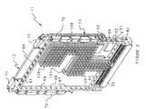
- Figure 2 is a back exploded perspective view of the wiring assembly of the present invention
- Figure 3 is a front perspective view of the wiring assembly of the present invention.
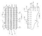
- Figure 4 is an enlarged, partial end view of the printed wiring board of the present invention.
- Figure 5 is a top plan view of a portion of the printed wiring board of the present invention.
- Figure 6 is a perspective view of a conduction and convention heat sink (for a die-up component) cantilevered from just one location on the assembly frame;
- Figure 7 is a perspective view of a conduction and convection heat sink (for a die-up component) cantilevered from two spaced apart locations on the assembly frame;
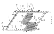
- Figure 8 is a perspective view of a conduction and convection heat sink (for a die-up component) suspended across the assembly frame;
- Figure 9 is a top plan view showing the wiring assembly of Figures 1 - 3 in an assembly having a cold wall.
- printed wiring assembly 11 includes a printed wiring board 13, a frame assembly 15, and an integrated conduction and convection heat sink 17.
- printed wiring board 13 (sometimes referred to as PWB) includes, inter alia , a top layer of insulating material 21, a bottom layer of insulating material 23 and thermally conductive layers 25 and 31.
- PWB 13 will, depending upon the complexity of the wired circuitry, include additional intermediate layers of signal, ground and power conductors, such as indicated by layers 27 and 29, all interspersed by layers of insulating material 33, 35 and 37.
- some layers have multiple functions (e.g., thermal and ground, thermal and power).
- the insulating materials can be of a variety of materials including polyimide, FR4, thermont, fiberglass, epoxy and combinations thereof.
- thermally conductive layer is made of at least 1 oz. copper, although the use of other thermally conductive materials is possible as will be apparent to those skilled in the art.
- thermally conductive layers 25 and 31 can be on the outside surface of layers 21 or 23.
- a variety of electronic components can be mounted on PWB13.
- die-up devices 41, 43, 45, 47 and 49 are mounted on PWB13.
- die-down devices 51 and 53 are also included.
- Die-up devices can include Motorola PPC603 P/N TSXP603PUAU8L, Tundra Real Image P/N M6458OWG, and Intel i960RP P/N GC80960RP3V33SL2GD; die-down devices can include Micrel Regulator P/N MIC 29301-SOBU, Analog Devices Voltage Reference P/N 5962-728022A, and Q-Tech Oscillator P/N QT66HC11-30.868 MHz.
- PWB 13 includes a connector 55, such as manufactured by Airborn P/N RM 422-196-192-9500-919.
- Frame assembly 15 includes frame portions 61, 63, 65 and 67 which, typically, form a rectangle although other configurations are possible.
- Aluminum is a preferred material. However, a variety of thermally conductive metals, composites and plastics can be used. As explained below, each portion includes a plurality of holes 69 for mounting one or more heat sinks 17.
- Assembly 15 also includes a pair of flanges 71 and 73 which, in turn, are used to mount wedgelocks 75 and card ejectors 77. Wedgelocks 75 are manufactured by Calmark (see, e.g., U.S. patent No. 4,819,713).
- Assembly 15 further includes, as best seen in Figure 2, three projections 81, 83 and 85, which are used to mount connector 55 to frame portion 65 and PWB 13.
- flanges 73 and 75 include a plurality of holes 91.
- PWB 13 and spacer strips 95 are secured to flanges 71 and 73 by a plurality of machine screws 93 or other fasteners which pass through openings in strips 95 (not shown), openings in PWB 13, holes 91, and are secured in tapped holes (not shown) provided in wedgelocks 75.
- Board 13 is also secured to projections 81, 83 and 85 by machine screws 97 which pass through holes 99 and are received in tapped holes (not shown) in connector 55.
- the thermal vias 100 which thermally couple, for instance, thermally conductive layer 25 to frame assembly 15 are illustrated.
- heat sink 17 is configured to overlay and thermally contact die-up devices 41, 43, 45, 47 and 49.
- Heat sink 17 which is made of aluminum or other suitable thermally conductive material, includes spaced apart portions 101, 103 and 105 which are adapted to be secured to frame portions 63 and 65, as illustrated in Figure 3, by machine screws (not shown) which are received in openings 69 and tapped openings 107.
- the thickness of heat sink 17 does not have to be uniform, but includes a series of planar surfaces 111, 113, 115, 117 and 119.
- This variation in thickness is determined by the various heights of the components above the top surface of printed wiring board 13, so that each surface is in close proximity the top surface of its associated component (i.e., 41, 43, 45, 47 and 49).
- a thermally conductive gap filling material e.g. aluminum oxide filled elastomers, thermally conductive grease, thermally conductive wax, thermally conductive epoxy
- Such gap filling materials are used to accommodate the height variational tolerances of the components.
- heat sink 17 conducts heat from devices 41, 43, 45, 47 and 49 to frame components 63 and 65.
- heat sink 17 can also be provided with a projection 121 having a surface 123 which engages the top surface of PWB 13 and is held in engagement therewith by machine screw 125 and cooperating tapped hole 127.
- the top surface is provided with a plurality of fins or pins 129.
- the size and shape of the heat sink is determined by the number and location of, for instance, die-up devices.
- Figure 6 illustrates a very simple cantilever mounted design 141, which is attached just to frame portion 67 by machine screws (not shown) received in, preferably, to two or more adjacent (or nearly adjacent) openings 69.
- Figure 7 illustrates an L-shaped heat sink 143 which is secured to frame member 63 by machine screws 145 and secured to frame member 61 by additional machine screws 145.
- Figure 8 illustrates heat sink 147 which bridges frame members 63 and 67. In its simplest form, it can be a simple, straight span.
- heat sink 147 has offset portions 149 (connected to frame member 63 via machine screws 145) and 151 (connected to frame member 67 via machine screws (not shown)). All the foregoing heat sinks include fins 129 for convection cooling.
- Heat sink 141 can be used alone, in connection with other cantilever heat sinks, or in connection with heat sinks 143 or 147. This permits the greatest flexibility in the design and layout of the components on printed wiring board 13, while permitting (in contrast to the arrangement disclosed by Tracy et al.) access to at least some, and preferably all of the components for inspection and/or electrical testing. It also allows for component placement and electrical design to occur independently of the heat sink design.
- heat sinks 17, 141, 143 and 147 cool die-up devices (and unpackaged electronic devices such as Micro Rel Driver L154C) by both convection cooling (via fins 129) and conduction cooling to the frame assembly 15.
- the die-down devices are cooled via conductive layers 25 and 31 to frame assembly 15.
- printed wiring assembly 11 is received in chassis 161, such as used in avionics, ground, ship and space applications.
- Chassis 161 includes card guides 165 and 167, and cold walls 169 and 171.
- Convection cooling is provided by moving air across fins 129. This could be achieved by natural convection or forced air. Forced air could be supplied by internal air movers (not shown) or external systems (not shown).
- Conduction cooling is achieved by the mechanical (and thermal) contact between frame assembly 15 (including wedgelocks 75) and the card guides 165, 167 provided on housing 161.
- Card guides 165, 167 are, in turn coupled to cold walls 169, 171.
- cold walls include one or more mechanisms by which heat is dissipated (e.g. secondary forced air, forced liquid cooling) from the attachment interface (not shown).
Landscapes
- Engineering & Computer Science (AREA)
- Microelectronics & Electronic Packaging (AREA)
- Physics & Mathematics (AREA)
- Thermal Sciences (AREA)
- Aviation & Aerospace Engineering (AREA)
- Cooling Or The Like Of Electrical Apparatus (AREA)
- Cooling Or The Like Of Semiconductors Or Solid State Devices (AREA)
Applications Claiming Priority (3)
| Application Number | Priority Date | Filing Date | Title |
|---|---|---|---|
| US09/460,196 US6239972B1 (en) | 1999-12-13 | 1999-12-13 | Integrated convection and conduction heat sink for multiple mounting positions |
| US460196 | 1999-12-13 | ||
| PCT/US2000/033532 WO2001047333A2 (en) | 1999-12-13 | 2000-12-11 | Integrated convection and conduction heat sink for multiple mounting positions |
Publications (2)
| Publication Number | Publication Date |
|---|---|
| EP1238574A2 EP1238574A2 (en) | 2002-09-11 |
| EP1238574B1 true EP1238574B1 (en) | 2003-05-14 |
Family
ID=23827734
Family Applications (1)
| Application Number | Title | Priority Date | Filing Date |
|---|---|---|---|
| EP00986314A Expired - Lifetime EP1238574B1 (en) | 1999-12-13 | 2000-12-11 | Integrated convection and conduction heat sink for multiple mounting positions |
Country Status (14)
| Country | Link |
|---|---|
| US (1) | US6239972B1 (da) |
| EP (1) | EP1238574B1 (da) |
| JP (1) | JP2003518761A (da) |
| KR (1) | KR20020061000A (da) |
| AT (1) | ATE240632T1 (da) |
| AU (1) | AU769351B2 (da) |
| CA (1) | CA2394064A1 (da) |
| DE (1) | DE60002758T2 (da) |
| DK (1) | DK1238574T3 (da) |
| ES (1) | ES2195950T3 (da) |
| IL (2) | IL150185A0 (da) |
| NZ (1) | NZ520138A (da) |
| TW (1) | TW499829B (da) |
| WO (1) | WO2001047333A2 (da) |
Families Citing this family (39)
| Publication number | Priority date | Publication date | Assignee | Title |
|---|---|---|---|---|
| US6320723B1 (en) * | 1999-06-24 | 2001-11-20 | Seagate Technology Llc | Protective cover for a disc drive printed circuit board wherein the cover and a circuit board component are thermally connected |
| US6426466B1 (en) * | 2000-02-09 | 2002-07-30 | International Business Machines Corporation | Peripheral power board structure |
| US6545871B1 (en) * | 2000-10-27 | 2003-04-08 | Thomson Licensing, S.A. | Apparatus for providing heat dissipation for a circuit element |
| US6377463B1 (en) * | 2000-12-12 | 2002-04-23 | Intel Corporation | Retention module for processor and chipset thermal solutions |
| US6639801B2 (en) * | 2001-08-10 | 2003-10-28 | Agilent Technologies, Inc. | Mechanical packaging architecture for heat dissipation |
| GB0200138D0 (en) * | 2002-01-04 | 2002-02-20 | Pace Micro Tech Plc | A holder for electrical apparatus |
| US6873528B2 (en) * | 2002-05-28 | 2005-03-29 | Dy 4 Systems Ltd. | Supplemental heat conduction path for card to chassis heat dissipation |
| US6659168B1 (en) * | 2002-07-09 | 2003-12-09 | Hewlett-Packard Development Company, L.P. | Heatsink with multiple fin types |
| US6975511B1 (en) * | 2002-07-18 | 2005-12-13 | Rockwell Collins | Ruggedized electronic module cooling system |
| US6741466B1 (en) | 2002-07-18 | 2004-05-25 | Rockwell Collins | Modular electronics system chassis |
| US6771508B1 (en) * | 2003-02-14 | 2004-08-03 | Intel Corporation | Method and apparatus for cooling an electronic component |
| US7027299B2 (en) * | 2003-08-19 | 2006-04-11 | Sun Microsystems, Inc. | Electronics assembly with arrangement for air cooling |
| JP4371210B2 (ja) * | 2003-12-05 | 2009-11-25 | 日本電気株式会社 | 電子ユニットおよびその放熱構造 |
| US7113406B1 (en) * | 2004-07-22 | 2006-09-26 | Cisco Technology, Inc. | Methods and apparatus for fastening a set of heatsinks to a circuit board |
| CN100379333C (zh) * | 2004-11-15 | 2008-04-02 | 广达电脑股份有限公司 | 散热装置 |
| US20060232928A1 (en) * | 2005-04-19 | 2006-10-19 | Vinson Wade D | Heat sink for multiple components |
| JP4617209B2 (ja) * | 2005-07-07 | 2011-01-19 | 株式会社豊田自動織機 | 放熱装置 |
| US7462934B2 (en) * | 2006-06-20 | 2008-12-09 | Microsoft Corporation | Integrated heat sink |
| JP4796457B2 (ja) * | 2006-08-16 | 2011-10-19 | 富士通株式会社 | 機器、演算装置および放熱部材 |
| US20080060789A1 (en) * | 2006-09-12 | 2008-03-13 | Chang Sob Lee | Heat transfer plate with retainer assembly |
| US7492598B2 (en) * | 2006-09-20 | 2009-02-17 | Cisco Technology, Inc. | Heatsink attachment mechanism |
| US9380726B2 (en) * | 2007-05-22 | 2016-06-28 | James Charles Calder | Retainer and thermal displacement apparatus for electronic components, methods of production and applications thereof |
| US8082978B2 (en) * | 2007-08-07 | 2011-12-27 | Georgia Tech Research Corporation | Fluid-to-fluid spot-to-spreader heat management devices and systems and methods of managing heat |
| CN101907908B (zh) * | 2009-06-04 | 2013-03-13 | 富准精密工业(深圳)有限公司 | 电子设备及其机箱 |
| US8456846B2 (en) * | 2010-01-20 | 2013-06-04 | Wavetherm Corporation | Wedge based circuit board retainer |
| US8270172B2 (en) * | 2010-04-23 | 2012-09-18 | GE Intelligent Platforms Embedded Systems, Inc. | Wedge lock for use with a single board computer, a single board computer, and method of assembling a computer system |
| DE102011107316A1 (de) * | 2011-07-06 | 2013-06-06 | Abb Ag | Anordnung zum Kühlen von Baugruppen eines Automatisierungs- oder Steuerungssystems |
| US9417670B2 (en) | 2012-08-07 | 2016-08-16 | Lockheed Martin Corporation | High power dissipation mezzanine card cooling frame |
| US9125299B2 (en) * | 2012-12-06 | 2015-09-01 | Apple Inc. | Cooling for electronic components |
| US9223167B2 (en) | 2013-06-26 | 2015-12-29 | Apple Inc. | Liquid crystal switching barrier thermal control |
| US9389029B2 (en) | 2013-09-30 | 2016-07-12 | Apple Inc. | Heat transfer structure |
| CN105700646A (zh) * | 2014-11-27 | 2016-06-22 | 英业达科技有限公司 | 服务器 |
| US9674986B2 (en) | 2015-08-03 | 2017-06-06 | Apple Inc. | Parallel heat spreader |
| US10794637B2 (en) | 2016-10-03 | 2020-10-06 | Ge Aviation Systems Llc | Circular heatsink |
| US11259445B2 (en) | 2020-03-05 | 2022-02-22 | Hamilton Sundstrand Corporation | Cooling mechanism for electrionic component mounted on a printed wiring board |
| CN111800979B (zh) * | 2020-05-13 | 2021-09-07 | 浙江众合科技股份有限公司 | 一种用于板卡测试的随用随取式板卡储存装置 |
| CN111487650B (zh) * | 2020-05-14 | 2022-07-26 | 国网河北省电力有限公司沧州供电分公司 | 一种对数据采集变电站进行巡检用的定位装置 |
| US20230224387A1 (en) | 2022-01-10 | 2023-07-13 | Apple Inc. | Handheld electronic device |
| US12610490B2 (en) | 2024-02-12 | 2026-04-21 | Wavetherm Corporation | Wedge based circuit board retainer with dual end drivescrew |
Family Cites Families (27)
| Publication number | Priority date | Publication date | Assignee | Title |
|---|---|---|---|---|
| US3467891A (en) * | 1967-10-03 | 1969-09-16 | Gen Electric | Combination electrical,mechanical,and thermal connector assembly |
| US4441140A (en) * | 1980-11-20 | 1984-04-03 | Raytheon Company | Printed circuit board holder |
| US4819713A (en) * | 1987-04-23 | 1989-04-11 | Calmark Corporation | Retainer for electronic modules |
| US4971570A (en) | 1989-08-31 | 1990-11-20 | Hughes Aircraft Company | Wedge clamp thermal connector |
| DE69025624T2 (de) * | 1989-12-22 | 1996-10-24 | The Foxboro Co., Foxboro, Mass. | Leichte anordnung für versiegelte schaltungsplatte |
| US5220485A (en) | 1990-04-18 | 1993-06-15 | Harris Corporation | Heat removing edge guide system and related method |
| DE9006916U1 (de) * | 1990-06-20 | 1991-10-24 | Robert Bosch Gmbh, 70469 Stuttgart | Gehäuse für eine elektronische Schaltung |
| FR2669178B1 (fr) | 1990-11-09 | 1996-07-26 | Merlin Gerin | Coffre et carte electronique a drain thermique et procede de fabrication d'une telle carte. |
| US5258887A (en) * | 1992-06-15 | 1993-11-02 | Eaton Corporation | Electrical device cooling system using a heat sink attached to a circuit board containing heat conductive layers and channels |
| US5276585A (en) | 1992-11-16 | 1994-01-04 | Thermalloy, Inc. | Heat sink mounting apparatus |
| JPH06309532A (ja) | 1993-04-26 | 1994-11-04 | Mitsubishi Electric Corp | Icカード |
| EP0633608B1 (en) | 1993-07-08 | 2000-10-11 | Sumitomo Metal Industries, Ltd. | Process for producing a pin-finned heat sink |
| US5385175A (en) | 1993-11-01 | 1995-01-31 | Intevep, S.A. | Conduit having hydrophilic and oleophobic inner surfaces for oil transportation |
| US5615735A (en) | 1994-09-29 | 1997-04-01 | Hewlett-Packard Co. | Heat sink spring clamp |
| US5472353A (en) | 1995-04-13 | 1995-12-05 | Hristake; Val | Isobaric expandable thermal clamp for printed circuit board |
| US5542468A (en) | 1995-06-28 | 1996-08-06 | Lin; Chuen-Sheng | CPU heat dissipator hook-up apparatus |
| US5831829A (en) | 1996-07-18 | 1998-11-03 | Lin; Mike | Heat dissipating device for central processing units |
| DE19632545A1 (de) * | 1996-08-13 | 1998-02-19 | Bodenseewerk Geraetetech | Elektronisches Gerät in Modulbauweise |
| US5930115A (en) | 1996-08-26 | 1999-07-27 | Compaq Computer Corp. | Apparatus, method and system for thermal management of a semiconductor device |
| US5815371A (en) | 1996-09-26 | 1998-09-29 | Dell U.S.A., L.P. | Multi-function heat dissipator |
| US5959350A (en) | 1997-05-21 | 1999-09-28 | Hon Hai Precision Ind. Co., Ltd. | Fixing device for securing a heat sink to a CPU module |
| US5835349A (en) * | 1997-06-12 | 1998-11-10 | Harris Corporation | Printed circuit board-mounted, sealed heat exchanger |
| TW335191U (en) | 1997-07-15 | 1998-06-21 | Hon Hai Prec Ind Co Ltd | Securing device |
| US5886821A (en) | 1997-10-02 | 1999-03-23 | Fresnel Technologies, Inc. | Lens assembly for miniature motion sensor |
| US5898750A (en) | 1998-01-23 | 1999-04-27 | Framatome Technologies | Nested sleeve grid restraint system |
| US6104613A (en) * | 1998-05-12 | 2000-08-15 | Lockheed Martin Federal Systems, Inc. | VME eurocard double printed wiring card host circuit card circuit (module) assembly |
| US5999407A (en) * | 1998-10-22 | 1999-12-07 | Lockheed Martin Corp. | Electronic module with conductively heat-sunk components |
-
1999
- 1999-12-13 US US09/460,196 patent/US6239972B1/en not_active Expired - Lifetime
-
2000
- 2000-12-11 DK DK00986314T patent/DK1238574T3/da active
- 2000-12-11 AU AU22581/01A patent/AU769351B2/en not_active Ceased
- 2000-12-11 DE DE60002758T patent/DE60002758T2/de not_active Expired - Fee Related
- 2000-12-11 EP EP00986314A patent/EP1238574B1/en not_active Expired - Lifetime
- 2000-12-11 IL IL15018500A patent/IL150185A0/xx unknown
- 2000-12-11 WO PCT/US2000/033532 patent/WO2001047333A2/en not_active Ceased
- 2000-12-11 NZ NZ520138A patent/NZ520138A/en unknown
- 2000-12-11 AT AT00986314T patent/ATE240632T1/de not_active IP Right Cessation
- 2000-12-11 JP JP2001547934A patent/JP2003518761A/ja not_active Withdrawn
- 2000-12-11 CA CA002394064A patent/CA2394064A1/en not_active Abandoned
- 2000-12-11 ES ES00986314T patent/ES2195950T3/es not_active Expired - Lifetime
- 2000-12-11 KR KR1020027007612A patent/KR20020061000A/ko not_active Withdrawn
-
2001
- 2001-02-21 TW TW089126472A patent/TW499829B/zh not_active IP Right Cessation
-
2002
- 2002-06-11 IL IL150185A patent/IL150185A/en unknown
Also Published As
| Publication number | Publication date |
|---|---|
| AU2258101A (en) | 2001-07-03 |
| ATE240632T1 (de) | 2003-05-15 |
| US6239972B1 (en) | 2001-05-29 |
| DE60002758D1 (de) | 2003-06-18 |
| NZ520138A (en) | 2003-10-31 |
| KR20020061000A (ko) | 2002-07-19 |
| CA2394064A1 (en) | 2001-06-28 |
| DE60002758T2 (de) | 2004-04-08 |
| WO2001047333A3 (en) | 2002-01-17 |
| WO2001047333A2 (en) | 2001-06-28 |
| EP1238574A2 (en) | 2002-09-11 |
| DK1238574T3 (da) | 2003-07-21 |
| IL150185A0 (en) | 2002-12-01 |
| AU769351B2 (en) | 2004-01-22 |
| ES2195950T3 (es) | 2003-12-16 |
| IL150185A (en) | 2006-04-10 |
| JP2003518761A (ja) | 2003-06-10 |
| TW499829B (en) | 2002-08-21 |
Similar Documents
| Publication | Publication Date | Title |
|---|---|---|
| EP1238574B1 (en) | Integrated convection and conduction heat sink for multiple mounting positions | |
| US6816378B1 (en) | Stack up assembly | |
| US5812387A (en) | Multi-deck power converter module | |
| US4771365A (en) | Passive cooled electronic chassis | |
| US5969949A (en) | Interfitting heat sink and heat spreader slug | |
| CA1210519A (en) | Circuit module with enhanced heat transfer and distribution | |
| US7855891B1 (en) | Modular heat sinks for housings for electronic equipment | |
| US5615086A (en) | Apparatus for cooling a plurality of electrical components mounted on a printed circuit board | |
| EP0448686B1 (en) | High-speed ccd sensor mounting system with improved signal to noise operation and thermal contact | |
| US6606246B2 (en) | Method and apparatus for retaining cooling apparatus and bus bar | |
| US20040218375A1 (en) | Thermal interface adapter plate conversion kit and method | |
| US7145774B2 (en) | Backside cooling apparatus for modular platforms | |
| US5198887A (en) | Semiconductor chip carrier | |
| US12035509B2 (en) | Assembly with a heat sink core element forming a supporting structure | |
| EP0741507B1 (en) | Arrangement for integrated circuits and a method for mounting the same |
Legal Events
| Date | Code | Title | Description |
|---|---|---|---|
| PUAI | Public reference made under article 153(3) epc to a published international application that has entered the european phase |
Free format text: ORIGINAL CODE: 0009012 |
|
| 17P | Request for examination filed |
Effective date: 20020618 |
|
| AK | Designated contracting states |
Kind code of ref document: A2 Designated state(s): AT BE CH CY DE DK ES FI FR GB GR IE IT LI LU MC NL PT SE TR |
|
| AX | Request for extension of the european patent |
Free format text: AL;LT;LV;MK;RO;SI |
|
| GRAH | Despatch of communication of intention to grant a patent |
Free format text: ORIGINAL CODE: EPIDOS IGRA |
|
| GRAH | Despatch of communication of intention to grant a patent |
Free format text: ORIGINAL CODE: EPIDOS IGRA |
|
| GRAA | (expected) grant |
Free format text: ORIGINAL CODE: 0009210 |
|
| AK | Designated contracting states |
Designated state(s): AT BE CH CY DE DK ES FI FR GB GR IE IT LI LU MC NL PT SE TR |
|
| PG25 | Lapsed in a contracting state [announced via postgrant information from national office to epo] |
Ref country code: IT Free format text: LAPSE BECAUSE OF FAILURE TO SUBMIT A TRANSLATION OF THE DESCRIPTION OR TO PAY THE FEE WITHIN THE PRESCRIBED TIME-LIMIT;WARNING: LAPSES OF ITALIAN PATENTS WITH EFFECTIVE DATE BEFORE 2007 MAY HAVE OCCURRED AT ANY TIME BEFORE 2007. THE CORRECT EFFECTIVE DATE MAY BE DIFFERENT FROM THE ONE RECORDED. Effective date: 20030514 Ref country code: FI Free format text: LAPSE BECAUSE OF FAILURE TO SUBMIT A TRANSLATION OF THE DESCRIPTION OR TO PAY THE FEE WITHIN THE PRESCRIBED TIME-LIMIT Effective date: 20030514 Ref country code: LI Free format text: LAPSE BECAUSE OF FAILURE TO SUBMIT A TRANSLATION OF THE DESCRIPTION OR TO PAY THE FEE WITHIN THE PRESCRIBED TIME-LIMIT Effective date: 20030514 Ref country code: TR Free format text: LAPSE BECAUSE OF FAILURE TO SUBMIT A TRANSLATION OF THE DESCRIPTION OR TO PAY THE FEE WITHIN THE PRESCRIBED TIME-LIMIT Effective date: 20030514 Ref country code: NL Free format text: LAPSE BECAUSE OF FAILURE TO SUBMIT A TRANSLATION OF THE DESCRIPTION OR TO PAY THE FEE WITHIN THE PRESCRIBED TIME-LIMIT Effective date: 20030514 Ref country code: AT Free format text: LAPSE BECAUSE OF FAILURE TO SUBMIT A TRANSLATION OF THE DESCRIPTION OR TO PAY THE FEE WITHIN THE PRESCRIBED TIME-LIMIT Effective date: 20030514 Ref country code: CH Free format text: LAPSE BECAUSE OF FAILURE TO SUBMIT A TRANSLATION OF THE DESCRIPTION OR TO PAY THE FEE WITHIN THE PRESCRIBED TIME-LIMIT Effective date: 20030514 |
|
| REG | Reference to a national code |
Ref country code: GB Ref legal event code: FG4D |
|
| REG | Reference to a national code |
Ref country code: CH Ref legal event code: EP |
|
| REG | Reference to a national code |
Ref country code: IE Ref legal event code: FG4D |
|
| REF | Corresponds to: |
Ref document number: 60002758 Country of ref document: DE Date of ref document: 20030618 Kind code of ref document: P |
|
| REG | Reference to a national code |
Ref country code: DK Ref legal event code: T3 |
|
| REG | Reference to a national code |
Ref country code: SE Ref legal event code: TRGR |
|
| PG25 | Lapsed in a contracting state [announced via postgrant information from national office to epo] |
Ref country code: PT Free format text: LAPSE BECAUSE OF FAILURE TO SUBMIT A TRANSLATION OF THE DESCRIPTION OR TO PAY THE FEE WITHIN THE PRESCRIBED TIME-LIMIT Effective date: 20030814 Ref country code: GR Free format text: LAPSE BECAUSE OF FAILURE TO SUBMIT A TRANSLATION OF THE DESCRIPTION OR TO PAY THE FEE WITHIN THE PRESCRIBED TIME-LIMIT Effective date: 20030814 |
|
| NLV1 | Nl: lapsed or annulled due to failure to fulfill the requirements of art. 29p and 29m of the patents act | ||
| REG | Reference to a national code |
Ref country code: CH Ref legal event code: PL |
|
| PG25 | Lapsed in a contracting state [announced via postgrant information from national office to epo] |
Ref country code: IE Free format text: LAPSE BECAUSE OF NON-PAYMENT OF DUE FEES Effective date: 20031211 Ref country code: CY Free format text: LAPSE BECAUSE OF FAILURE TO SUBMIT A TRANSLATION OF THE DESCRIPTION OR TO PAY THE FEE WITHIN THE PRESCRIBED TIME-LIMIT Effective date: 20031211 Ref country code: LU Free format text: LAPSE BECAUSE OF NON-PAYMENT OF DUE FEES Effective date: 20031211 |
|
| REG | Reference to a national code |
Ref country code: ES Ref legal event code: FG2A Ref document number: 2195950 Country of ref document: ES Kind code of ref document: T3 |
|
| PG25 | Lapsed in a contracting state [announced via postgrant information from national office to epo] |
Ref country code: MC Free format text: LAPSE BECAUSE OF NON-PAYMENT OF DUE FEES Effective date: 20031231 |
|
| ET | Fr: translation filed | ||
| PLBE | No opposition filed within time limit |
Free format text: ORIGINAL CODE: 0009261 |
|
| STAA | Information on the status of an ep patent application or granted ep patent |
Free format text: STATUS: NO OPPOSITION FILED WITHIN TIME LIMIT |
|
| 26N | No opposition filed |
Effective date: 20040217 |
|
| REG | Reference to a national code |
Ref country code: IE Ref legal event code: MM4A |
|
| PGFP | Annual fee paid to national office [announced via postgrant information from national office to epo] |
Ref country code: DK Payment date: 20061108 Year of fee payment: 7 |
|
| PGFP | Annual fee paid to national office [announced via postgrant information from national office to epo] |
Ref country code: FR Payment date: 20061201 Year of fee payment: 7 |
|
| PGFP | Annual fee paid to national office [announced via postgrant information from national office to epo] |
Ref country code: SE Payment date: 20061204 Year of fee payment: 7 |
|
| PGFP | Annual fee paid to national office [announced via postgrant information from national office to epo] |
Ref country code: ES Payment date: 20061222 Year of fee payment: 7 |
|
| PGFP | Annual fee paid to national office [announced via postgrant information from national office to epo] |
Ref country code: DE Payment date: 20061229 Year of fee payment: 7 |
|
| REG | Reference to a national code |
Ref country code: DK Ref legal event code: EBP |
|
| EUG | Se: european patent has lapsed | ||
| PG25 | Lapsed in a contracting state [announced via postgrant information from national office to epo] |
Ref country code: SE Free format text: LAPSE BECAUSE OF NON-PAYMENT OF DUE FEES Effective date: 20071212 Ref country code: DE Free format text: LAPSE BECAUSE OF NON-PAYMENT OF DUE FEES Effective date: 20080701 |
|
| REG | Reference to a national code |
Ref country code: FR Ref legal event code: ST Effective date: 20081020 |
|
| PG25 | Lapsed in a contracting state [announced via postgrant information from national office to epo] |
Ref country code: DK Free format text: LAPSE BECAUSE OF NON-PAYMENT OF DUE FEES Effective date: 20080102 |
|
| REG | Reference to a national code |
Ref country code: ES Ref legal event code: FD2A Effective date: 20071212 |
|
| PG25 | Lapsed in a contracting state [announced via postgrant information from national office to epo] |
Ref country code: FR Free format text: LAPSE BECAUSE OF NON-PAYMENT OF DUE FEES Effective date: 20071231 Ref country code: ES Free format text: LAPSE BECAUSE OF NON-PAYMENT OF DUE FEES Effective date: 20071212 |
|
| PGFP | Annual fee paid to national office [announced via postgrant information from national office to epo] |
Ref country code: BE Payment date: 20090112 Year of fee payment: 9 |
|
| BERE | Be: lapsed |
Owner name: *HONEYWELL INTERNATIONAL INC. Effective date: 20091231 |
|
| PG25 | Lapsed in a contracting state [announced via postgrant information from national office to epo] |
Ref country code: BE Free format text: LAPSE BECAUSE OF NON-PAYMENT OF DUE FEES Effective date: 20091231 |
|
| PGFP | Annual fee paid to national office [announced via postgrant information from national office to epo] |
Ref country code: GB Payment date: 20141124 Year of fee payment: 15 |
|
| GBPC | Gb: european patent ceased through non-payment of renewal fee |
Effective date: 20151211 |
|
| PG25 | Lapsed in a contracting state [announced via postgrant information from national office to epo] |
Ref country code: GB Free format text: LAPSE BECAUSE OF NON-PAYMENT OF DUE FEES Effective date: 20151211 |