EP1243569A2 - Elektrische Schaltung mit einem metallgebundenen Keramik Material oder MGK Komponent als isolierendes Substrat - Google Patents
Elektrische Schaltung mit einem metallgebundenen Keramik Material oder MGK Komponent als isolierendes Substrat Download PDFInfo
- Publication number
- EP1243569A2 EP1243569A2 EP02012565A EP02012565A EP1243569A2 EP 1243569 A2 EP1243569 A2 EP 1243569A2 EP 02012565 A EP02012565 A EP 02012565A EP 02012565 A EP02012565 A EP 02012565A EP 1243569 A2 EP1243569 A2 EP 1243569A2
- Authority
- EP
- European Patent Office
- Prior art keywords
- metal
- mbc
- ceramic
- ceramic member
- aluminum
- Prior art date
- Legal status (The legal status is an assumption and is not a legal conclusion. Google has not performed a legal analysis and makes no representation as to the accuracy of the status listed.)
- Withdrawn
Links
Images


Classifications
-
- C—CHEMISTRY; METALLURGY
- C04—CEMENTS; CONCRETE; ARTIFICIAL STONE; CERAMICS; REFRACTORIES
- C04B—LIME, MAGNESIA; SLAG; CEMENTS; COMPOSITIONS THEREOF, e.g. MORTARS, CONCRETE OR LIKE BUILDING MATERIALS; ARTIFICIAL STONE; CERAMICS; REFRACTORIES; TREATMENT OF NATURAL STONE
- C04B41/00—After-treatment of mortars, concrete, artificial stone or ceramics; Treatment of natural stone
- C04B41/009—After-treatment of mortars, concrete, artificial stone or ceramics; Treatment of natural stone characterised by the material treated
-
- C—CHEMISTRY; METALLURGY
- C04—CEMENTS; CONCRETE; ARTIFICIAL STONE; CERAMICS; REFRACTORIES
- C04B—LIME, MAGNESIA; SLAG; CEMENTS; COMPOSITIONS THEREOF, e.g. MORTARS, CONCRETE OR LIKE BUILDING MATERIALS; ARTIFICIAL STONE; CERAMICS; REFRACTORIES; TREATMENT OF NATURAL STONE
- C04B37/00—Joining burned ceramic articles with other burned ceramic articles or other articles by heating
- C04B37/02—Joining burned ceramic articles with other burned ceramic articles or other articles by heating with metallic articles
-
- B—PERFORMING OPERATIONS; TRANSPORTING
- B22—CASTING; POWDER METALLURGY
- B22D—CASTING OF METALS; CASTING OF OTHER SUBSTANCES BY THE SAME PROCESSES OR DEVICES
- B22D19/00—Casting in, on, or around objects which form part of the product
- B22D19/14—Casting in, on, or around objects which form part of the product the objects being filamentary or particulate in form
-
- C—CHEMISTRY; METALLURGY
- C04—CEMENTS; CONCRETE; ARTIFICIAL STONE; CERAMICS; REFRACTORIES
- C04B—LIME, MAGNESIA; SLAG; CEMENTS; COMPOSITIONS THEREOF, e.g. MORTARS, CONCRETE OR LIKE BUILDING MATERIALS; ARTIFICIAL STONE; CERAMICS; REFRACTORIES; TREATMENT OF NATURAL STONE
- C04B41/00—After-treatment of mortars, concrete, artificial stone or ceramics; Treatment of natural stone
- C04B41/45—Coating or impregnating, e.g. injection in masonry, partial coating of green or fired ceramics, organic coating compositions for adhering together two concrete elements
- C04B41/4505—Coating or impregnating, e.g. injection in masonry, partial coating of green or fired ceramics, organic coating compositions for adhering together two concrete elements characterised by the method of application
- C04B41/4523—Coating or impregnating, e.g. injection in masonry, partial coating of green or fired ceramics, organic coating compositions for adhering together two concrete elements characterised by the method of application applied from the molten state ; Thermal spraying, e.g. plasma spraying
-
- C—CHEMISTRY; METALLURGY
- C04—CEMENTS; CONCRETE; ARTIFICIAL STONE; CERAMICS; REFRACTORIES
- C04B—LIME, MAGNESIA; SLAG; CEMENTS; COMPOSITIONS THEREOF, e.g. MORTARS, CONCRETE OR LIKE BUILDING MATERIALS; ARTIFICIAL STONE; CERAMICS; REFRACTORIES; TREATMENT OF NATURAL STONE
- C04B41/00—After-treatment of mortars, concrete, artificial stone or ceramics; Treatment of natural stone
- C04B41/45—Coating or impregnating, e.g. injection in masonry, partial coating of green or fired ceramics, organic coating compositions for adhering together two concrete elements
- C04B41/50—Coating or impregnating, e.g. injection in masonry, partial coating of green or fired ceramics, organic coating compositions for adhering together two concrete elements with inorganic materials
- C04B41/51—Metallising, e.g. infiltration of sintered ceramic preforms with molten metal
-
- C—CHEMISTRY; METALLURGY
- C04—CEMENTS; CONCRETE; ARTIFICIAL STONE; CERAMICS; REFRACTORIES
- C04B—LIME, MAGNESIA; SLAG; CEMENTS; COMPOSITIONS THEREOF, e.g. MORTARS, CONCRETE OR LIKE BUILDING MATERIALS; ARTIFICIAL STONE; CERAMICS; REFRACTORIES; TREATMENT OF NATURAL STONE
- C04B41/00—After-treatment of mortars, concrete, artificial stone or ceramics; Treatment of natural stone
- C04B41/80—After-treatment of mortars, concrete, artificial stone or ceramics; Treatment of natural stone of only ceramics
- C04B41/81—Coating or impregnation
-
- C—CHEMISTRY; METALLURGY
- C04—CEMENTS; CONCRETE; ARTIFICIAL STONE; CERAMICS; REFRACTORIES
- C04B—LIME, MAGNESIA; SLAG; CEMENTS; COMPOSITIONS THEREOF, e.g. MORTARS, CONCRETE OR LIKE BUILDING MATERIALS; ARTIFICIAL STONE; CERAMICS; REFRACTORIES; TREATMENT OF NATURAL STONE
- C04B41/00—After-treatment of mortars, concrete, artificial stone or ceramics; Treatment of natural stone
- C04B41/80—After-treatment of mortars, concrete, artificial stone or ceramics; Treatment of natural stone of only ceramics
- C04B41/81—Coating or impregnation
- C04B41/85—Coating or impregnation with inorganic materials
- C04B41/88—Metals
-
- C—CHEMISTRY; METALLURGY
- C23—COATING METALLIC MATERIAL; COATING MATERIAL WITH METALLIC MATERIAL; CHEMICAL SURFACE TREATMENT; DIFFUSION TREATMENT OF METALLIC MATERIAL; COATING BY VACUUM EVAPORATION, BY SPUTTERING, BY ION IMPLANTATION OR BY CHEMICAL VAPOUR DEPOSITION, IN GENERAL; INHIBITING CORROSION OF METALLIC MATERIAL OR INCRUSTATION IN GENERAL
- C23C—COATING METALLIC MATERIAL; COATING MATERIAL WITH METALLIC MATERIAL; SURFACE TREATMENT OF METALLIC MATERIAL BY DIFFUSION INTO THE SURFACE, BY CHEMICAL CONVERSION OR SUBSTITUTION; COATING BY VACUUM EVAPORATION, BY SPUTTERING, BY ION IMPLANTATION OR BY CHEMICAL VAPOUR DEPOSITION, IN GENERAL
- C23C2/00—Hot-dipping or immersion processes for applying the coating material in the molten state without affecting the shape; Apparatus therefor
- C23C2/006—Pattern or selective deposits
- C23C2/0062—Pattern or selective deposits without pre-treatment of the material to be coated, e.g. using masking elements such as casings, shields, fixtures or blocking elements
-
- C—CHEMISTRY; METALLURGY
- C23—COATING METALLIC MATERIAL; COATING MATERIAL WITH METALLIC MATERIAL; CHEMICAL SURFACE TREATMENT; DIFFUSION TREATMENT OF METALLIC MATERIAL; COATING BY VACUUM EVAPORATION, BY SPUTTERING, BY ION IMPLANTATION OR BY CHEMICAL VAPOUR DEPOSITION, IN GENERAL; INHIBITING CORROSION OF METALLIC MATERIAL OR INCRUSTATION IN GENERAL
- C23C—COATING METALLIC MATERIAL; COATING MATERIAL WITH METALLIC MATERIAL; SURFACE TREATMENT OF METALLIC MATERIAL BY DIFFUSION INTO THE SURFACE, BY CHEMICAL CONVERSION OR SUBSTITUTION; COATING BY VACUUM EVAPORATION, BY SPUTTERING, BY ION IMPLANTATION OR BY CHEMICAL VAPOUR DEPOSITION, IN GENERAL
- C23C2/00—Hot-dipping or immersion processes for applying the coating material in the molten state without affecting the shape; Apparatus therefor
- C23C2/04—Hot-dipping or immersion processes for applying the coating material in the molten state without affecting the shape; Apparatus therefor characterised by the coating material
- C23C2/12—Aluminium or alloys based thereon
-
- C—CHEMISTRY; METALLURGY
- C23—COATING METALLIC MATERIAL; COATING MATERIAL WITH METALLIC MATERIAL; CHEMICAL SURFACE TREATMENT; DIFFUSION TREATMENT OF METALLIC MATERIAL; COATING BY VACUUM EVAPORATION, BY SPUTTERING, BY ION IMPLANTATION OR BY CHEMICAL VAPOUR DEPOSITION, IN GENERAL; INHIBITING CORROSION OF METALLIC MATERIAL OR INCRUSTATION IN GENERAL
- C23C—COATING METALLIC MATERIAL; COATING MATERIAL WITH METALLIC MATERIAL; SURFACE TREATMENT OF METALLIC MATERIAL BY DIFFUSION INTO THE SURFACE, BY CHEMICAL CONVERSION OR SUBSTITUTION; COATING BY VACUUM EVAPORATION, BY SPUTTERING, BY ION IMPLANTATION OR BY CHEMICAL VAPOUR DEPOSITION, IN GENERAL
- C23C2/00—Hot-dipping or immersion processes for applying the coating material in the molten state without affecting the shape; Apparatus therefor
- C23C2/34—Hot-dipping or immersion processes for applying the coating material in the molten state without affecting the shape; Apparatus therefor characterised by the shape of the material to be treated
- C23C2/36—Elongated material
-
- C—CHEMISTRY; METALLURGY
- C23—COATING METALLIC MATERIAL; COATING MATERIAL WITH METALLIC MATERIAL; CHEMICAL SURFACE TREATMENT; DIFFUSION TREATMENT OF METALLIC MATERIAL; COATING BY VACUUM EVAPORATION, BY SPUTTERING, BY ION IMPLANTATION OR BY CHEMICAL VAPOUR DEPOSITION, IN GENERAL; INHIBITING CORROSION OF METALLIC MATERIAL OR INCRUSTATION IN GENERAL
- C23C—COATING METALLIC MATERIAL; COATING MATERIAL WITH METALLIC MATERIAL; SURFACE TREATMENT OF METALLIC MATERIAL BY DIFFUSION INTO THE SURFACE, BY CHEMICAL CONVERSION OR SUBSTITUTION; COATING BY VACUUM EVAPORATION, BY SPUTTERING, BY ION IMPLANTATION OR BY CHEMICAL VAPOUR DEPOSITION, IN GENERAL
- C23C30/00—Coating with metallic material characterised only by the composition of the metallic material, i.e. not characterised by the coating process
-
- H—ELECTRICITY
- H05—ELECTRIC TECHNIQUES NOT OTHERWISE PROVIDED FOR
- H05K—PRINTED CIRCUITS; CASINGS OR CONSTRUCTIONAL DETAILS OF ELECTRIC APPARATUS; MANUFACTURE OF ASSEMBLAGES OF ELECTRICAL COMPONENTS
- H05K3/00—Apparatus or processes for manufacturing printed circuits
- H05K3/0058—Laminating printed circuit boards onto other substrates, e.g. metallic substrates
- H05K3/0061—Laminating printed circuit boards onto other substrates, e.g. metallic substrates onto a metallic substrate, e.g. a heat sink
-
- H—ELECTRICITY
- H10—SEMICONDUCTOR DEVICES; ELECTRIC SOLID-STATE DEVICES NOT OTHERWISE PROVIDED FOR
- H10W—GENERIC PACKAGES, INTERCONNECTIONS, CONNECTORS OR OTHER CONSTRUCTIONAL DETAILS OF DEVICES COVERED BY CLASS H10
- H10W40/00—Arrangements for thermal protection or thermal control
- H10W40/20—Arrangements for cooling
- H10W40/25—Arrangements for cooling characterised by their materials
- H10W40/255—Arrangements for cooling characterised by their materials having a laminate or multilayered structure, e.g. direct bond copper [DBC] ceramic substrates
-
- H—ELECTRICITY
- H10—SEMICONDUCTOR DEVICES; ELECTRIC SOLID-STATE DEVICES NOT OTHERWISE PROVIDED FOR
- H10W—GENERIC PACKAGES, INTERCONNECTIONS, CONNECTORS OR OTHER CONSTRUCTIONAL DETAILS OF DEVICES COVERED BY CLASS H10
- H10W70/00—Package substrates; Interposers; Redistribution layers [RDL]
- H10W70/01—Manufacture or treatment
- H10W70/02—Manufacture or treatment of conductive package substrates serving as an interconnection, e.g. of metal plates
-
- C—CHEMISTRY; METALLURGY
- C04—CEMENTS; CONCRETE; ARTIFICIAL STONE; CERAMICS; REFRACTORIES
- C04B—LIME, MAGNESIA; SLAG; CEMENTS; COMPOSITIONS THEREOF, e.g. MORTARS, CONCRETE OR LIKE BUILDING MATERIALS; ARTIFICIAL STONE; CERAMICS; REFRACTORIES; TREATMENT OF NATURAL STONE
- C04B2111/00—Mortars, concrete or artificial stone or mixtures to prepare them, characterised by specific function, property or use
- C04B2111/00474—Uses not provided for elsewhere in C04B2111/00
- C04B2111/00844—Uses not provided for elsewhere in C04B2111/00 for electronic applications
-
- H—ELECTRICITY
- H05—ELECTRIC TECHNIQUES NOT OTHERWISE PROVIDED FOR
- H05K—PRINTED CIRCUITS; CASINGS OR CONSTRUCTIONAL DETAILS OF ELECTRIC APPARATUS; MANUFACTURE OF ASSEMBLAGES OF ELECTRICAL COMPONENTS
- H05K1/00—Printed circuits
- H05K1/02—Details
- H05K1/0271—Arrangements for reducing stress or warp in rigid printed circuit boards, e.g. caused by loads, vibrations or differences in thermal expansion
-
- H—ELECTRICITY
- H05—ELECTRIC TECHNIQUES NOT OTHERWISE PROVIDED FOR
- H05K—PRINTED CIRCUITS; CASINGS OR CONSTRUCTIONAL DETAILS OF ELECTRIC APPARATUS; MANUFACTURE OF ASSEMBLAGES OF ELECTRICAL COMPONENTS
- H05K1/00—Printed circuits
- H05K1/02—Details
- H05K1/03—Use of materials for the substrate
- H05K1/0306—Inorganic insulating substrates, e.g. ceramic, glass
Definitions
- This invention relates to a process for producing rugged metal-bonded-ceramic (MBC) material or components, particularly to an industrial process for producing MBC material or components of metals with oxide, nitride or carbide ceramics that are suitable for use in automotive parts, electronic parts, etc.
- MBC rugged metal-bonded-ceramic
- the invention also relates to MBC plates produced by that process, as well as electronic circuit substrates fabricated from said MBC plates.
- MBC components are extensively used in automobiles, electronic equipment and other applications by taking advantages of the chemical stability, high melting points, insulating property and high hardness of ceramics in combination with the high strength, high toughness, free workability and conducting property of metals.
- Typical applications of the components include rotors for automotive turbochargers, as well as substrates and packages for mounting large-power electronic elements.
- MBC material and components are known to be produced by various methods including adhesion, plating, metallizing, thermal spraying, brazing, DBC, shrink fitting and casting.
- Adhesion is a process in which a metal member is joined to a ceramic member with an organic or inorganic adhesive.
- Plating is a process that comprises activating the surface of a ceramic member and dipping it in a plating bath to apply a metal plate.
- Metallizing is a process that comprises applying a paste containing metal particles to the surface of a ceramic member and sintering it to form metal layer.
- Thermal spraying is a process in which molten metal (or ceramic) drops are sprayed onto the surface of a ceramic (or metal) member so that a metal (or ceramic) layer is formed on that surface.
- Brazing is a process in which metal and a ceramic member are joined with the aid of a low-melting point filler metal or alloy.
- a metal component highly reactive with ceramics is added or metal layer is preliminarily formed on the joining surface of the ceramic member by a suitable method such as metallizing or thermal spraying.
- DBC is a technique specially developed for the purpose of bonding an oxide ceramic member to a copper member. According to DBC, an oxygen containing copper member is heated in an inert atmosphere while it is joined to the ceramic member or, alternatively, the surface of an oxygen-free copper plate is first oxidized to form an oxide layer and then it is joined to the ceramic member.
- an oxide layer must be formed preliminarily on the surface of the nonoxide ceramic member.
- the ceramic and metal members to be joined are provided with a projection and a cavity, respectively, in such a way that the outside diameter of the projection is equal to the inside diameter of the cavity and the metal member is heated to expand the cavity, into which the projection of the ceramic member is inserted; thereafter, the two members are cooled so that they form an integral assembly in which the projection on the ceramic member is nested in the cavity in the metal member.
- Casting is similar to shrink fitting, except that a metal is cast around a ceramic member and cooled so that it shrinks to have the ceramic member nested as an integral part.
- Adhesion produces composites that are low in adhesion strength and heat resistance.
- the applicability of plating, metallizing and thermal spraying is usually limited to the case of forming thin metal (or ceramic) layers whose thickness ranges from a few microns to several tens of microns.
- Shrink fitting and casting are only applicable to a special case in which at least part of a ceramic member is to be nested in a metal.
- copper is the only metal that can be joined and the temperature for jointing must be within a narrow range close to the eutectic point of Cu-O and, hence, there is high likelihood for the development of joining defects such as swelling and incomplete joining.
- Brazing uses expensive filler metals or alloys and requires the joining operation to be performed in vacuum and, hence, the operational cost is high enough to prevent the use of the method in a broad range of applications.
- MBC components can be used as substrates for mounting large-power electronic elements.
- MBC substrates comprise ceramic substrates having copper circuit patterns formed on the surface.
- commercial composite substrates are classified as copper/alumina directly joined substrates, copper/aluminum nitride directly joined substrates, copper/alumina brazed substrates and copper/aluminum nitride brazed substrates.
- a method for producing copper/alumina directly joined substrates is described in Unexamined Published Japanese Patent Application (kokai) Sho-52-37914; an oxygen-containing copper plate is superposed on an alumina substrate or, alternatively, an oxygen-free copper plate is heated in an oxidizing atmosphere to generate copper oxide on the surface of the oxygen-free copper plate before the copper plate is joined to the alumina substrate with a composite oxide of copper and aluminum being formed at the interface.
- an oxide must first be formed on the surface of an aluminum nitride substrate.
- a method of production is described in Unexamined Published Japanese Patent Application (kokai) Hei 3-93687; the aluminum nitride substrate is first treated in air at a temperature of about 1,000°C to form an oxide layer on the surface and, then, a copper plate is joined to the aluminum nitride substrate with the intermediary of the oxide layer by the method described in the preceding paragraph.
- a copper plate is joined to a ceramic substrate with the aid of a low-melting point filler metal.
- a commonly used filler metal is made from an alloy comprising Ag, Cu and Ti. In this case the purpose of adding Ag is to lower the melting point and that of adding Ti is to enhance the wettability of the filler metal to ceramics.
- the latter When mounting electronic elements on MBC substrates, the latter are heated to about 400°C and also the temperature of the MBC substrate will change all the time due to the temperature change in the operating environment or due to the generation of heat during the use of the assembled electronic devices, whereby the MBC substrates are subjected to varying thermal stresses. On account of these thermal stresses, cracks will develop in the ceramic substrate.
- An important factor to the evaluation of the MBC substrates is resistance to heat cycles. This factor is expressed by the number of times a substrate can be subjected to repeated heating and cooling cycles between -40°C and 125°C without developing cracks due to thermal stresses.
- the copper-bonded-ceramic substrates can only withstand several tens heat cycles under the indicated conditions. What is more, in order to acquire the resistance to the heat cycles, the thickness of the ceramic substrate has to be greater than the sum of the thicknesses of copper plates joined to both principal surfaces of the ceramic substrate. This means that the thickness of the ceramic substrate must be increased beyond the value necessary to maintain its inherent electrical insulating property. As a result, heat conduction which is another important characteristic of the MBC substrates is sacrificed.
- Aluminum is as good an electric and heat conductor as copper and the idea of using it as a conductive circuit material is easy to be conceived, as typicaly described in Unexamined Published Japanese Patent Application (kokai) Sho 59-121890.
- brazing is used to join aluminum and ceramics and Unexamined Published Japanese Patent Applications (kokai) Hei 3-125463, Hei 4-12554 and Hei 4-18746 teach aluminum-ceramic substrates produced by brazing. These substrates can withstand about 200 heat cycles but they are still unsuitable for use on electric cars and in other applications where very high resistance to heat cycles is required.
- brazing must be conducted in vacuum and nonoxide ceramics must be subjected to a preliminary treatment for forming an oxide on the surface and this makes the brazing process unsatisfactory in terms of not only production cost but also heat conduction.
- the present invention has been accomplished to solve these problems of the prior art and has as an object providing a process by which MBC material or components of many various shapes having improved characteristics can be manufactured at low cost.
- Another object of the invention is to provide MBC plates produced by that process.
- a further object of the invention is to provide MBC electronic circuit substrates that are fabricated from said MBC plates.
- the present inventors conducted intensive studies with a view to attaining these objects and found an effective method of bonding molten metals to ceramics, as well as an effective method of shaping metals.
- the present invention has been accomplished on the basis of these findings.
- the present invention is directed to
- the present process for producing MBC material or MBC components 5 having a metal joined to at least part of ceramic members 2 is characterized in that the ceramic members 2 are moved as they are kept in contact with the melt 1 of the metal so that they are wetted by the melt, followed by cooling so that the melt solidifies on the surface of the ceramic members 2 to be joined to the latter.
- the ceramic member 2 is moved as the part thereof to be joined to the metal is kept in contact with the melt 1 of the metal so that it is wetted by the melt 1 and, thereafter, the metal melt 1 or part thereof is allowed to solidify in a selected area of the ceramic member 2 so that a metal part of a predetermined shape will form.
- the ceramic member 2 is supplied continuously to the metal melt 1 and moved as the part thereof to be joined to the metal is kept in contact with the metal melt 1 so that it is wetted by the metal melt 1 and, thereafter, the ceramic member 2 is recovered so that part of the metal melt 1 solidifies in a selected area of the ceramic member 2 to form a metal part of a predetermined shape.
- that part of the ceramic member 2 to be joined to the metal is fed continuously into the metal melt 1 from one side thereof and, after it is wetted fully by the metal melt 1, the ceramic member 2 is passed through a die 6B in the opposite direction so that part of the metal melt 1 solidifies in a selected area of the ceramic member 2 to form a metal part of a predetermined shape.
- the ceramic portion of the MBC material or a component that has a metal joined preliminarily to part of the ceramic member 2 is fed into the melt of a joining metal having a lower melting point than the joined metal from one side thereof and, after it is wetted fully by the metal melt, the ceramic portion is passed through the die 6B in the opposite direction so that part of the low-melting point metal melt solidifies in a selected area of the MBC material or a component having the high-melting point metal joined thereto, thereby forming a low-melting point metal part of a predetermined shape.
- the ceramic member or portion is made of an oxide, a nitride or a carbide.
- the metal is aluminum, copper, iron, nickel, silver or gold or an alloy based on one of these metals.
- the present invention provides a MBC plate member characterized in that a metal plate is formed on a ceramic substrate by any one of the processes described above.
- the present invention provides a MBC electronic circuit substrate characterized in that a predetemined circuit pattern is formed by etching the metal plate of the MBC plate member described above.
- Metals are joined to ceramics in one of three modes, mechanical, physical and chemical, which are designated according to the joining mechanism involved.
- Mechanical joining is achieved when a projection on a ceramic member is nested in a cavity in a metal member by a mechanical force as in the case of joining the two members by shrink fitting or casting; mechanical joining is also achieved if, as in the case of adhesion, an adhesive gets into recesses in the surfaces of the ceramic and metal members to exhibit an "anchor" effect when cured, thus producing an integral assembly of the metal and ceramic members.
- Physical joining is achieved by the force of attraction (van der Waals forces) acting between the molecules of a ceramic member and metal atoms.
- Chemical joining is achieved by covalent bonding (sharing) or ionic bonding (transfer) between electrons within a ceramic molecule and those in a metal atom. Since chemical bonding is established if electronic sharing or transfer occurs between surface molecules (electrons) of a ceramic and a metal member, reaction products that can be discovered by physical means (e.g. common optical microscope, SEMs and TEMs) will not necessarily exist at the interface between the ceramic and metal members. In this case, it is often difficult to distinguish physical joining from chemical joining solely in view of the state of the interface. As a matter of fact, there are many cases where several joining mechanisms occur simultaneously at the interface between the members to be joined but in order to achieve reliable joining, it is essential that either phycical or chemical joining be accomplished.
- the state of wetting is investigated by the following simpler and more practical procedure. That is, the ceramic member 2 is brought into contact with the metal melt 1 which has been heated at a given temperature; after the lapse of a certain time, the ceramic member 2 is taken out of the melt 1; the metal that adheres loosely to the cooled surface of the ceramic member 2 is scraped off and the state of wetting of the ceramic member 2 by the metal is investigated.
- the first step of achieving physical or chemical joining is cleaning the surfaces of the members to be joined.
- reference 1 Japanese Patent application Hei 4-355211
- one of the present inventors proposed a method of cleaning the surfaces of the members to be joined.
- the ceramic member 2 is inserted into the metal melt 1 or the latter is cast in a mold with the ceramic member 2 being presetted in it, thereby creating a relative movement between the melt 1 and the ceramic member 2 to produce a clean interface between the melt and the ceramic member so that the metal can be joined securely to the ceramic member.
- the present inventors conducted intensive studies on the basis of this proposal and found an industrial process for producing MBC material or components 5 having many various shapes.
- the process comprises the steps of (1) inserting the ceramic member 2 into the metal melt 1 by moving the former through the later until at least part of the ceramic member 2 that is to be joined to the metal is wetted by the metal melt 1 and (2) recovering the ceramic member 2 from the metal melt 1 by passing it through a die 6 worked to a predetermined shape, so that part of the metal melt 1 solidifies in a predetermined shape in a predetermined area of the ceramic member 2.
- the surface cleaning does not necessarily mean the removal of all ingredients other than the components from which the members to be joined are made.
- the ingredients are capable of promoting physical or chemical joining, such capability should be positively utilized.
- the surface of nonoxide ceramic member has to be oxidized so that an oxide layer is formed.
- the purpose of "cleaning" in the present invention is limited to removing any ingredients that can be harmful to the creation of physical or chemical joining.
- Fig. 2 is a diagram showing the basic concept of the invention. If the ceramic member 2 is to be moved through the metal melt only a small distance, it is insufficient to assure complete removal of the deleterious ingredient 4 on the surface of the ceramic member and the deleterious ingredient 3 on the surface of the metal melt; as a result, part of the ceramic member 2 remains unwetted by the metal 1, making it impossible to accomplish secure joining between the ceramic member and the metal. In order to avoid this incomplete joining, the distance over which the ceramic member 2 is moved through the metal melt 1 must exceed a certain minimum value (Dmin).
- Dmin certain minimum value
- the minimum distance (Dmin) ranges from a few millimeters to several tens of millimeters.
- Example 1 there is disclosed an exemplary process for producing the MBC material 5.
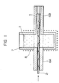
- Fig. 1 is a schematic section of the apparatus for implementing the process and
- Fig. 3 is a sectional view showing the cross section of the die 6.
- the ceramic member 2 is fed successively into the molten metal 1 through the guide 6A linked to the die 6B and, after being thoroughly wetted by the melt, exits from the die 6B to form a metal part of a predetermined shape in a predetemined area of the ceramic member 2.
- the resulting MBC material 5 is structurally integral if the dimension of the melt in the moving direction of the ceramic member 2 is set to be longer than the minimum distance required for the ceramic member 2 to be wetted by the melt.
- the melt and the ceramic member 2 are made of aluminum and alumina, respectively, but it should also be understood in the light of the above-described spirit of the invention that they are by no means limited to aluminum and alumina. Combinations of other metals and ceramics may equally be applicable as long as the ceramic member 2 can be wetted by the molten metal 1.
- the ceramic member 2 need not even be wetted by certain metals only if it can be modified or wetting accelerators can be added to the metals so as to improve the wetting of the ceramic member 2 by the molten metal 1. This method is also applicable to the invention with good results.
- the surface of the ceramic member may preliminarily be oxidized to form an oxide such as alumina, or the molten copper is exposed to air, supplemented with copper oxide or otherwise treated to incorporate oxygen, whereby the wetting of the ceramic member 2 with the molten copper is sufficiently improved to ensure the production of a composite in which the ceramic member 2 is securely joined to the metal part.
- an alumina-silver composite a similarly strong joint can be obtained by adding titanium or other active metals to the molten silver.
- the temperature, the atmosphere and the rate of movement of the ceramic member 2 are very important parameters for the purposes of the present invention.
- different metals and ceramic members 2 have different characteristics and, hence, these parameters are variable with what members are to be joined.
- These conditions should be selected in such a way that the ceramic member 2 will be effectively wetted by the molten metal 1. The proper selection of these conditions is an important step for assuring that the advantages of the invention will be exhibited to the fullest extent.
- the present inventors could produce MBC plate members and they could also fabricate MBC electronic circuit substrates by etching the metal portion of the MBC plate members.
- the MBC plate members produced by the process of the invention has to be seperated by shearing at the connecting portions of the ceramic substrates and it is also necessary to form resist patterns on a polished surface of the metal portion.
- Resist patterns can be formed by various method; in one method, a light-sensitive resist film is compressed onto the surface of the metal portion, exposed to light through an overlying pattern mask, and developed to remove the resist in the unwanted areas; alternatively, a layer of liquid resist is printed in a predetermined pattern directly onto the metal and exposed to UV light to cure the resist. After these pretreatments, an etching solution is sprayed onto the composite substrate having the resist patterns formed thereon and the metal is removed from the resist-free areas to form metal circuit patterns of the predetermined shapes.
- alumina and aluminum nitride substrates were used as ceramic substrates but it is contemplated that other ceramic substrates made of silicon carbide, zirconia, etc., as well as various glass substrates are also applicable with equally good results.
- the metal to be composited with the ceramic member pure aluminum metal was used since it was a good electric conductor that would also insure softness.
- the purity of the aluminum used was 99.9% (3N) in order to achieve a balance between the electric conductivity (which increases with the purity) and the price.
- 3N the purity of the aluminum used was 99.9%
- the experimental setup shown in Fig. 1 was used; the die 6B on the exit side had the cross section shown in Fig. 3.
- Aluminum was set in a crucible 7. Alumina plates were fed from the inlet into the guide 6A and it was set in such a way that its forward end would protrude a little from the inner surface of the crucible 7.
- the crucible 7 was heated in a nitrogen (N 2 ) gas atmosphere to melt the aluminum.
- N 2 nitrogen
- the clearance has to be smaller than a certain value; in Example 1, the clearance was set to be smaller than 0.1 mm.
- Example 1 the minimum distance Dmin over which each alumina plate moved until it was wetted by aluminum melt was measured with the heating temperature, extruding temperature and the flow rate of nitrogen gas being set at various values. Samples were sliced from the thus prepared aluminum-bonded-alumina plates and evaluated by the method described in Reference 1, supra (Japanese Patent Application Hei 4-355211). For Dmin measurement, the crucible 7 was emptied of the melt and the alumina plate was recovered and the distance between the point where it started to contact the aluminum melt and the area that was completely wetted by the melt was measured. The results are shown in Table 1 for the samples prepared. All samples except Lot E were characterized by a dense aluminum structure and had peel strengths in excess of 35 kg/cm.
- Aluminum-bonded-alumina plates having heat-dissipating fins 10 (see Fig. 4) on one side were produced by repeating the procedure of-Example 1 except for the following points: the die 6B on the exit side had an interior as shown in cross section in Fig. 4; the melt temperature, extrusion speed and the flow rate of nitrogen gas were set at 850°C, 25 mm/min and 30L/min, respectively; a pressure of 0.5 kg/cm 2 was applied to the melt to accelerate its run and to prevent the formation of cavities.
- the MBC material thus produced had satisfactory quality.
- MBC material having copper plates on one side and aluminum heat-dissipating fins 10 on the other side were produced by repeating the procedure of Example 2 except for the following points: the alumina plates had a copper plate joined to one surface by DBC; the guide in the melt was worked to have the cross-sectional shape shown in Fig. 5. The MBC material thus produced had satisfactory quality.
- MBC components having aluminum fins joined to the circumference of ceramic pipes were produced by repeating the procedure of Example 2 except for the following points: a plurality of alumina pipes each having an outside diameter of 50 mm, a wall thickness of 5 mm and a length of 500 mm were provided as ceramic members; the die profile was changed from a rectangular to a circular shape; and the cross section of the die 6B was changed from the shape shown in Fig. 3 to that shown in Fig. 6.
- Aluminum-bonded-alumina plates were produced by repeating the procedure of Example 1 except that a plurality of alumina substrates 0.635 mm thick having breaking lines as shown in Fig. 7 were provided as ceramic substrates. Each MBC member was broken apart in the connecting portions and the surface of the metal portion was polished in preparation for resist formation.
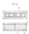
- each MBC substrate was sprayed with a liquid etchant in the form of an aqueous solution of a mixture of 35% 40 Be iron chloride and 10% HCl, whereby circuit patterns of the geometries shown in Fig. 8 were formed on opposite sides of MBC substrate.
- the surfaces of the circuit patterns were subjected to a treatment for zinc replacement and a nickel plate was deposited in a thickness of 3 - 5 ⁇ m.
- the thus fabricated composite substrate was split along the breaking lines to yield two aluminum-bonded-alumina electronic circuit substrates each having a width of 26 mm and a length of 51 mm.
- the MBC substrates were found to have the following characteristics:
- Aluminum-bonded-aluminum nitride directly joined substrates were produced by repeating the procedure of Example 6 except that the alumina substrates were replaced by aluminum nitride plates measuring 36 mm'x 52 mm x 0.635 mm.
- the MBC substrates thus produced had the following characteristics:
- the process of the present invention one can produce satisfactory MBC material or components 5 of many various shapes at low cost.
- the invention also provides MBC electronic circuit substrates having satisfactory characteristics.
Landscapes
- Chemical & Material Sciences (AREA)
- Engineering & Computer Science (AREA)
- Organic Chemistry (AREA)
- Ceramic Engineering (AREA)
- Materials Engineering (AREA)
- Mechanical Engineering (AREA)
- Metallurgy (AREA)
- Chemical Kinetics & Catalysis (AREA)
- Structural Engineering (AREA)
- Inorganic Chemistry (AREA)
- Physics & Mathematics (AREA)
- Plasma & Fusion (AREA)
- Manufacturing & Machinery (AREA)
- Microelectronics & Electronic Packaging (AREA)
- Ceramic Products (AREA)
- Insulated Metal Substrates For Printed Circuits (AREA)
- Parts Printed On Printed Circuit Boards (AREA)
Applications Claiming Priority (3)
| Application Number | Priority Date | Filing Date | Title |
|---|---|---|---|
| JP6096941A JP2918191B2 (ja) | 1994-04-11 | 1994-04-11 | 金属−セラミックス複合部材の製造方法 |
| JP9694194 | 1994-04-11 | ||
| EP95105372A EP0676800B1 (de) | 1994-04-11 | 1995-04-10 | Prozess zur Herstellung von metallbondiertem Keramikmaterial oder Komponente und dessen Verwendung als Substrat für eine elektronische Schaltung |
Related Parent Applications (2)
| Application Number | Title | Priority Date | Filing Date |
|---|---|---|---|
| EP95105372.7 Division | 1995-04-10 | ||
| EP95105372A Division EP0676800B1 (de) | 1994-04-11 | 1995-04-10 | Prozess zur Herstellung von metallbondiertem Keramikmaterial oder Komponente und dessen Verwendung als Substrat für eine elektronische Schaltung |
Publications (2)
| Publication Number | Publication Date |
|---|---|
| EP1243569A2 true EP1243569A2 (de) | 2002-09-25 |
| EP1243569A3 EP1243569A3 (de) | 2008-11-19 |
Family
ID=14178356
Family Applications (2)
| Application Number | Title | Priority Date | Filing Date |
|---|---|---|---|
| EP95105372A Expired - Lifetime EP0676800B1 (de) | 1994-04-11 | 1995-04-10 | Prozess zur Herstellung von metallbondiertem Keramikmaterial oder Komponente und dessen Verwendung als Substrat für eine elektronische Schaltung |
| EP02012565A Withdrawn EP1243569A3 (de) | 1994-04-11 | 1995-04-10 | Elektrische Schaltung mit einem metallgebundenen Keramik Material oder MGK Komponent als isolierendes Substrat |
Family Applications Before (1)
| Application Number | Title | Priority Date | Filing Date |
|---|---|---|---|
| EP95105372A Expired - Lifetime EP0676800B1 (de) | 1994-04-11 | 1995-04-10 | Prozess zur Herstellung von metallbondiertem Keramikmaterial oder Komponente und dessen Verwendung als Substrat für eine elektronische Schaltung |
Country Status (6)
| Country | Link |
|---|---|
| EP (2) | EP0676800B1 (de) |
| JP (1) | JP2918191B2 (de) |
| KR (1) | KR100201887B1 (de) |
| CN (2) | CN1246902C (de) |
| DE (1) | DE69529185T2 (de) |
| MY (1) | MY114268A (de) |
Families Citing this family (31)
| Publication number | Priority date | Publication date | Assignee | Title |
|---|---|---|---|---|
| JPH08330507A (ja) * | 1995-05-30 | 1996-12-13 | Motorola Inc | ハイブリッド・マルチチップ・モデュールおよびその製造方法 |
| AT405039B (de) * | 1996-02-08 | 1999-04-26 | Electrovac | Verbundbauteil |
| DE19735531A1 (de) * | 1997-08-16 | 1999-02-18 | Abb Research Ltd | Leistungshalbleitermodul mit in Submodulen integrierten Kühlern |
| JP4756200B2 (ja) * | 2000-09-04 | 2011-08-24 | Dowaメタルテック株式会社 | 金属セラミックス回路基板 |
| JP4434545B2 (ja) | 2001-03-01 | 2010-03-17 | Dowaホールディングス株式会社 | 半導体実装用絶縁基板及びパワーモジュール |
| JP4692708B2 (ja) | 2002-03-15 | 2011-06-01 | Dowaメタルテック株式会社 | セラミックス回路基板およびパワーモジュール |
| JP4324704B2 (ja) | 2002-09-13 | 2009-09-02 | Dowaメタルテック株式会社 | 金属−セラミックス複合部材の製造装置、製造用鋳型、並びに製造方法 |
| JP4028452B2 (ja) * | 2003-08-27 | 2007-12-26 | Dowaホールディングス株式会社 | 電子部品搭載基板およびその製造方法 |
| JP4821013B2 (ja) * | 2003-09-29 | 2011-11-24 | Dowaメタルテック株式会社 | アルミニウム−セラミックス接合基板およびその製造方法 |
| JP4496404B2 (ja) * | 2003-10-10 | 2010-07-07 | Dowaメタルテック株式会社 | 金属−セラミックス接合基板およびその製造方法 |
| JP4543279B2 (ja) * | 2004-03-31 | 2010-09-15 | Dowaメタルテック株式会社 | アルミニウム接合部材の製造方法 |
| JP5467407B2 (ja) * | 2007-10-22 | 2014-04-09 | Dowaメタルテック株式会社 | アルミニウム−セラミックス接合体 |
| JP4862196B2 (ja) * | 2008-07-14 | 2012-01-25 | Dowaメタルテック株式会社 | 金属セラミックス回路基板の製造方法 |
| CN101538166B (zh) * | 2009-04-30 | 2014-01-29 | 清华大学 | 陶瓷和铝或铝合金的连接方法 |
| CN101538171B (zh) * | 2009-04-30 | 2014-09-17 | 清华大学 | 一种表面金属化陶瓷及其制造方法 |
| US9061943B2 (en) * | 2009-04-30 | 2015-06-23 | Tsinghua University | Method for metallizing ceramic surface and method for connecting ceramic with aluminum |
| US20100314790A1 (en) * | 2009-06-12 | 2010-12-16 | Stansberry Peter G | Highly Oriented Graphite Product |
| FR2969402B1 (fr) * | 2010-12-17 | 2013-02-15 | Fibercryst | Module a gain laser et methode de fabrication d'un tel module |
| DE102011103746A1 (de) | 2011-05-31 | 2012-12-06 | Ixys Semiconductor Gmbh | Verfahren zum Fügen von Metall-Keramik-Substraten an Metallkörpern |
| DE102012102611B4 (de) * | 2012-02-15 | 2017-07-27 | Rogers Germany Gmbh | Metall-Keramik-Substrat sowie Verfahren zum Herstellen eines Metall-Keramik-Substrates |
| DE102012103786B4 (de) * | 2012-04-30 | 2017-05-18 | Rogers Germany Gmbh | Metall-Keramik-Substrat sowie Verfahren zum Herstellen eines Metall-Keramik-Substrates |
| JP6233973B2 (ja) * | 2014-03-31 | 2017-11-22 | Dowaメタルテック株式会社 | 金属−セラミックス回路基板の製造方法 |
| FR3026845B1 (fr) * | 2014-10-07 | 2018-11-09 | Constellium Issoire | Procede de mouillage d'une sonotrode |
| JP2016048789A (ja) * | 2015-11-05 | 2016-04-07 | Dowaホールディングス株式会社 | アルミニウム−セラミックス接合体の製造方法 |
| CN108257922A (zh) * | 2016-12-29 | 2018-07-06 | 比亚迪股份有限公司 | 一种散热基板及其制备方法和应用以及电子元器件 |
| JP7202213B2 (ja) * | 2019-02-22 | 2023-01-11 | Dowaメタルテック株式会社 | 金属-セラミックス接合基板およびその製造方法 |
| JP7480533B2 (ja) * | 2020-03-10 | 2024-05-10 | 東ソー株式会社 | Cr-Si系焼結体 |
| JP2021165220A (ja) * | 2020-04-08 | 2021-10-14 | 住友金属鉱山シポレックス株式会社 | 軽量気泡コンクリートの製造方法 |
| CN112238587B (zh) * | 2020-08-26 | 2023-03-14 | 山东高速交通装备有限公司 | 一种复合材料组合梁挤出成型设备 |
| CN113443621A (zh) * | 2021-07-23 | 2021-09-28 | 哈尔滨六方新材料科技有限公司 | 一种镁基复合材料中纳米碳材料的回收方法 |
| CN118080821B (zh) * | 2024-04-23 | 2024-07-09 | 广州众山精密科技有限公司 | 一种铝液连铸制备的铜铝复合板料及其工艺 |
Citations (7)
| Publication number | Priority date | Publication date | Assignee | Title |
|---|---|---|---|---|
| JPS5237914A (en) | 1975-07-30 | 1977-03-24 | Gen Electric | Method of directly combining metal to ceramics and metal |
| JPS59121890A (ja) | 1982-12-28 | 1984-07-14 | 株式会社東芝 | セラミツクスと金属との接合体 |
| JPH0393687A (ja) | 1989-09-06 | 1991-04-18 | Toshiba Corp | 窒化アルミニウム基板の製造方法 |
| JPH03125463A (ja) | 1989-10-09 | 1991-05-28 | Mitsubishi Materials Corp | 半導体装置用軽量基板 |
| JPH0412554A (ja) | 1990-05-02 | 1992-01-17 | Mitsubishi Materials Corp | 半導体装置用軽量基板 |
| JPH0418746A (ja) | 1990-05-11 | 1992-01-22 | Mitsubishi Materials Corp | Ic実装用基板 |
| JPH04355211A (ja) | 1991-05-31 | 1992-12-09 | Matsushita Electric Ind Co Ltd | 磁気ヘッドおよびその製造方法 |
Family Cites Families (14)
| Publication number | Priority date | Publication date | Assignee | Title |
|---|---|---|---|---|
| FR2109254A5 (en) * | 1970-10-08 | 1972-05-26 | Inst Materia | Cermet prodn - by melt impregnation of a preheated porous ceramic body |
| US4104417A (en) * | 1973-03-12 | 1978-08-01 | Union Carbide Corporation | Method of chemically bonding aluminum to carbon substrates via monocarbides |
| US3994430A (en) * | 1975-07-30 | 1976-11-30 | General Electric Company | Direct bonding of metals to ceramics and metals |
| US4409278A (en) * | 1981-04-16 | 1983-10-11 | General Electric Company | Blister-free direct bonding of metals to ceramics and metals |
| JPS58138061A (ja) * | 1982-02-10 | 1983-08-16 | Sumitomo Electric Ind Ltd | Ic用基板 |
| DE3376829D1 (en) * | 1982-06-29 | 1988-07-07 | Toshiba Kk | Method for directly bonding ceramic and metal members and laminated body of the same |
| JPS6318648A (ja) * | 1986-07-11 | 1988-01-26 | Toshiba Corp | 窒化アルミニウム回路基板 |
| JPS63250022A (ja) * | 1987-04-03 | 1988-10-17 | Sumitomo Electric Ind Ltd | 超電導導体の製造方法 |
| JPS649884A (en) * | 1987-05-30 | 1989-01-13 | Ikuo Okamoto | Insert ceramics |
| DE3804124A1 (de) * | 1988-02-11 | 1989-08-17 | Htk Ges Fuer Hochtemperaturker | Verfahren zum herstellen eines gegenstands aus siliziumkarbid-keramik |
| JPH0676266B2 (ja) * | 1988-07-13 | 1994-09-28 | 日本碍子株式会社 | 酸化物超電導焼結体およびその製造方法 |
| FR2655334B1 (fr) * | 1989-12-06 | 1992-02-21 | Poudres & Explosifs Ste Nale | Procede de preparation de chlorures d'acides carboxyliques chlores. |
| US5213877A (en) * | 1991-05-02 | 1993-05-25 | Mitsubishi Materials Corporation | Ceramic substrate used for fabricating electric or electronic circuit |
| JPH075758A (ja) * | 1993-06-16 | 1995-01-10 | Ricoh Co Ltd | 現像装置 |
-
1994
- 1994-04-11 JP JP6096941A patent/JP2918191B2/ja not_active Expired - Fee Related
-
1995
- 1995-04-10 EP EP95105372A patent/EP0676800B1/de not_active Expired - Lifetime
- 1995-04-10 EP EP02012565A patent/EP1243569A3/de not_active Withdrawn
- 1995-04-10 DE DE69529185T patent/DE69529185T2/de not_active Expired - Lifetime
- 1995-04-11 CN CNB001287923A patent/CN1246902C/zh not_active Expired - Fee Related
- 1995-04-11 CN CN95104308A patent/CN1066494C/zh not_active Expired - Fee Related
- 1995-04-11 MY MYPI95000924A patent/MY114268A/en unknown
- 1995-04-11 KR KR1019950008428A patent/KR100201887B1/ko not_active Expired - Fee Related
Patent Citations (7)
| Publication number | Priority date | Publication date | Assignee | Title |
|---|---|---|---|---|
| JPS5237914A (en) | 1975-07-30 | 1977-03-24 | Gen Electric | Method of directly combining metal to ceramics and metal |
| JPS59121890A (ja) | 1982-12-28 | 1984-07-14 | 株式会社東芝 | セラミツクスと金属との接合体 |
| JPH0393687A (ja) | 1989-09-06 | 1991-04-18 | Toshiba Corp | 窒化アルミニウム基板の製造方法 |
| JPH03125463A (ja) | 1989-10-09 | 1991-05-28 | Mitsubishi Materials Corp | 半導体装置用軽量基板 |
| JPH0412554A (ja) | 1990-05-02 | 1992-01-17 | Mitsubishi Materials Corp | 半導体装置用軽量基板 |
| JPH0418746A (ja) | 1990-05-11 | 1992-01-22 | Mitsubishi Materials Corp | Ic実装用基板 |
| JPH04355211A (ja) | 1991-05-31 | 1992-12-09 | Matsushita Electric Ind Co Ltd | 磁気ヘッドおよびその製造方法 |
Also Published As
| Publication number | Publication date |
|---|---|
| EP0676800A2 (de) | 1995-10-11 |
| KR950032001A (ko) | 1995-12-20 |
| EP0676800B1 (de) | 2002-12-18 |
| DE69529185T2 (de) | 2003-09-25 |
| EP1243569A3 (de) | 2008-11-19 |
| DE69529185D1 (de) | 2003-01-30 |
| JPH07276035A (ja) | 1995-10-24 |
| MY114268A (en) | 2002-09-30 |
| CN1118382A (zh) | 1996-03-13 |
| JP2918191B2 (ja) | 1999-07-12 |
| KR100201887B1 (ko) | 1999-06-15 |
| CN1066494C (zh) | 2001-05-30 |
| EP0676800A3 (de) | 1997-01-15 |
| CN1332265A (zh) | 2002-01-23 |
| CN1246902C (zh) | 2006-03-22 |
Similar Documents
| Publication | Publication Date | Title |
|---|---|---|
| EP0676800B1 (de) | Prozess zur Herstellung von metallbondiertem Keramikmaterial oder Komponente und dessen Verwendung als Substrat für eine elektronische Schaltung | |
| US6183875B1 (en) | Electronic circuit substrates fabricated from an aluminum ceramic composite material | |
| US3766634A (en) | Method of direct bonding metals to non-metallic substrates | |
| US3993411A (en) | Bonds between metal and a non-metallic substrate | |
| EP1187198A2 (de) | Metallkeramik-Leiterplatte und ihre Herstellungsweise | |
| JP2003112242A (ja) | 金属成形体製造方法およびこれにより製造される金属成形体 | |
| EP1122780A2 (de) | Laminatkühler, Leistungshalbleiter und seine Herstellung | |
| KR100374379B1 (ko) | 기판 | |
| JP4124497B2 (ja) | 金属−セラミックス複合基板及びその製造法 | |
| JPH02500907A (ja) | セラミック・ガラス・金属複合体 | |
| JP3392594B2 (ja) | アルミニウム−セラミックス複合基板のエッチング処理方法およびエッチング液 | |
| JP3890540B2 (ja) | 金属−セラミックス複合基板及びその製造法 | |
| JP3452822B2 (ja) | アルミニウム−セラミックス複合部材の製造方法 | |
| JP3613759B2 (ja) | 金属−セラミックス複合基板 | |
| JPH11322455A (ja) | セラミックス/金属接合体およびその製造方法 | |
| Ning et al. | Interface of aluminum/ceramic power substrates manufactured by casting-bonding process | |
| JP3383892B2 (ja) | 半導体実装構造体の製造方法 | |
| CZ20256A3 (cs) | Způsob metalizace vodivého motivu z mědi na keramickém substrátu pro elektronické součástky a metalizovaný keramický substrát vytvořený tímto způsobem | |
| JPH107480A (ja) | 金属−セラミックス複合基板及びその製造法 | |
| JP4669965B2 (ja) | アルミニウム−セラミックス接合基板およびその製造方法 | |
| CZ38408U1 (cs) | Metalizovaný keramický substrát pro elektronické součástky | |
| JP3550212B2 (ja) | セラミックス電子回路基板の製造方法 | |
| Pietrzak | Carbon Fibre Reinforced Copper Matrix Composites for Electronic and Electronical Devices | |
| KR100213427B1 (ko) | 동복강선 및 그 제조방법 | |
| JP4493128B2 (ja) | アルミニウム−セラミックス質複合体製造用金型 |
Legal Events
| Date | Code | Title | Description |
|---|---|---|---|
| PUAI | Public reference made under article 153(3) epc to a published international application that has entered the european phase |
Free format text: ORIGINAL CODE: 0009012 |
|
| 17P | Request for examination filed |
Effective date: 20020702 |
|
| AC | Divisional application: reference to earlier application |
Ref document number: 676800 Country of ref document: EP |
|
| AK | Designated contracting states |
Kind code of ref document: A2 Designated state(s): DE GB |
|
| RAP1 | Party data changed (applicant data changed or rights of an application transferred) |
Owner name: DOWA HOLDINGS CO., LTD. |
|
| RAP1 | Party data changed (applicant data changed or rights of an application transferred) |
Owner name: DOWA METALTECH CO., LTD. |
|
| PUAL | Search report despatched |
Free format text: ORIGINAL CODE: 0009013 |
|
| AK | Designated contracting states |
Kind code of ref document: A3 Designated state(s): DE GB |
|
| RIC1 | Information provided on ipc code assigned before grant |
Ipc: C23C 2/00 20060101ALI20081014BHEP Ipc: B22D 19/14 20060101ALI20081014BHEP Ipc: C04B 41/88 20060101ALI20081014BHEP Ipc: H01L 23/373 20060101ALI20081014BHEP Ipc: H01L 21/48 20060101AFI20081014BHEP |
|
| AKX | Designation fees paid |
Designated state(s): DE GB |
|
| 17Q | First examination report despatched |
Effective date: 20090701 |
|
| STAA | Information on the status of an ep patent application or granted ep patent |
Free format text: STATUS: THE APPLICATION IS DEEMED TO BE WITHDRAWN |
|
| 18D | Application deemed to be withdrawn |
Effective date: 20121101 |