EP1249874A2 - Lichtemittierende Vorrichtung - Google Patents
Lichtemittierende Vorrichtung Download PDFInfo
- Publication number
- EP1249874A2 EP1249874A2 EP20020007367 EP02007367A EP1249874A2 EP 1249874 A2 EP1249874 A2 EP 1249874A2 EP 20020007367 EP20020007367 EP 20020007367 EP 02007367 A EP02007367 A EP 02007367A EP 1249874 A2 EP1249874 A2 EP 1249874A2
- Authority
- EP
- European Patent Office
- Prior art keywords
- light emitting
- semiconductor
- emitting element
- emitting device
- opening
- Prior art date
- Legal status (The legal status is an assumption and is not a legal conclusion. Google has not performed a legal analysis and makes no representation as to the accuracy of the status listed.)
- Withdrawn
Links
Images








Classifications
-
- H—ELECTRICITY
- H10—SEMICONDUCTOR DEVICES; ELECTRIC SOLID-STATE DEVICES NOT OTHERWISE PROVIDED FOR
- H10H—INORGANIC LIGHT-EMITTING SEMICONDUCTOR DEVICES HAVING POTENTIAL BARRIERS
- H10H20/00—Individual inorganic light-emitting semiconductor devices having potential barriers, e.g. light-emitting diodes [LED]
- H10H20/80—Constructional details
- H10H20/85—Packages
- H10H20/852—Encapsulations
- H10H20/854—Encapsulations characterised by their material, e.g. epoxy or silicone resins
-
- F—MECHANICAL ENGINEERING; LIGHTING; HEATING; WEAPONS; BLASTING
- F24—HEATING; RANGES; VENTILATING
- F24C—DOMESTIC STOVES OR RANGES ; DETAILS OF DOMESTIC STOVES OR RANGES, OF GENERAL APPLICATION
- F24C15/00—Details
- F24C15/20—Removing cooking fumes
- F24C15/2071—Removing cooking fumes mounting of cooking hood
-
- H—ELECTRICITY
- H10—SEMICONDUCTOR DEVICES; ELECTRIC SOLID-STATE DEVICES NOT OTHERWISE PROVIDED FOR
- H10H—INORGANIC LIGHT-EMITTING SEMICONDUCTOR DEVICES HAVING POTENTIAL BARRIERS
- H10H20/00—Individual inorganic light-emitting semiconductor devices having potential barriers, e.g. light-emitting diodes [LED]
- H10H20/80—Constructional details
- H10H20/85—Packages
- H10H20/857—Interconnections, e.g. lead-frames, bond wires or solder balls
-
- H—ELECTRICITY
- H10—SEMICONDUCTOR DEVICES; ELECTRIC SOLID-STATE DEVICES NOT OTHERWISE PROVIDED FOR
- H10W—GENERIC PACKAGES, INTERCONNECTIONS, CONNECTORS OR OTHER CONSTRUCTIONAL DETAILS OF DEVICES COVERED BY CLASS H10
- H10W90/00—Package configurations
-
- H—ELECTRICITY
- H10—SEMICONDUCTOR DEVICES; ELECTRIC SOLID-STATE DEVICES NOT OTHERWISE PROVIDED FOR
- H10H—INORGANIC LIGHT-EMITTING SEMICONDUCTOR DEVICES HAVING POTENTIAL BARRIERS
- H10H20/00—Individual inorganic light-emitting semiconductor devices having potential barriers, e.g. light-emitting diodes [LED]
- H10H20/80—Constructional details
- H10H20/83—Electrodes
- H10H20/831—Electrodes characterised by their shape
-
- H—ELECTRICITY
- H10—SEMICONDUCTOR DEVICES; ELECTRIC SOLID-STATE DEVICES NOT OTHERWISE PROVIDED FOR
- H10H—INORGANIC LIGHT-EMITTING SEMICONDUCTOR DEVICES HAVING POTENTIAL BARRIERS
- H10H20/00—Individual inorganic light-emitting semiconductor devices having potential barriers, e.g. light-emitting diodes [LED]
- H10H20/80—Constructional details
- H10H20/85—Packages
- H10H20/8506—Containers
-
- H—ELECTRICITY
- H10—SEMICONDUCTOR DEVICES; ELECTRIC SOLID-STATE DEVICES NOT OTHERWISE PROVIDED FOR
- H10H—INORGANIC LIGHT-EMITTING SEMICONDUCTOR DEVICES HAVING POTENTIAL BARRIERS
- H10H20/00—Individual inorganic light-emitting semiconductor devices having potential barriers, e.g. light-emitting diodes [LED]
- H10H20/80—Constructional details
- H10H20/85—Packages
- H10H20/851—Wavelength conversion means
- H10H20/8511—Wavelength conversion means characterised by their material, e.g. binder
-
- H—ELECTRICITY
- H10—SEMICONDUCTOR DEVICES; ELECTRIC SOLID-STATE DEVICES NOT OTHERWISE PROVIDED FOR
- H10H—INORGANIC LIGHT-EMITTING SEMICONDUCTOR DEVICES HAVING POTENTIAL BARRIERS
- H10H20/00—Individual inorganic light-emitting semiconductor devices having potential barriers, e.g. light-emitting diodes [LED]
- H10H20/80—Constructional details
- H10H20/85—Packages
- H10H20/852—Encapsulations
- H10H20/853—Encapsulations characterised by their shape
-
- H—ELECTRICITY
- H10—SEMICONDUCTOR DEVICES; ELECTRIC SOLID-STATE DEVICES NOT OTHERWISE PROVIDED FOR
- H10H—INORGANIC LIGHT-EMITTING SEMICONDUCTOR DEVICES HAVING POTENTIAL BARRIERS
- H10H20/00—Individual inorganic light-emitting semiconductor devices having potential barriers, e.g. light-emitting diodes [LED]
- H10H20/80—Constructional details
- H10H20/882—Scattering means
-
- H—ELECTRICITY
- H10—SEMICONDUCTOR DEVICES; ELECTRIC SOLID-STATE DEVICES NOT OTHERWISE PROVIDED FOR
- H10W—GENERIC PACKAGES, INTERCONNECTIONS, CONNECTORS OR OTHER CONSTRUCTIONAL DETAILS OF DEVICES COVERED BY CLASS H10
- H10W72/00—Interconnections or connectors in packages
- H10W72/071—Connecting or disconnecting
- H10W72/072—Connecting or disconnecting of bump connectors
- H10W72/07251—Connecting or disconnecting of bump connectors characterised by changes in properties of the bump connectors during connecting
-
- H—ELECTRICITY
- H10—SEMICONDUCTOR DEVICES; ELECTRIC SOLID-STATE DEVICES NOT OTHERWISE PROVIDED FOR
- H10W—GENERIC PACKAGES, INTERCONNECTIONS, CONNECTORS OR OTHER CONSTRUCTIONAL DETAILS OF DEVICES COVERED BY CLASS H10
- H10W72/00—Interconnections or connectors in packages
- H10W72/071—Connecting or disconnecting
- H10W72/072—Connecting or disconnecting of bump connectors
- H10W72/07251—Connecting or disconnecting of bump connectors characterised by changes in properties of the bump connectors during connecting
- H10W72/07252—Connecting or disconnecting of bump connectors characterised by changes in properties of the bump connectors during connecting changes in structures or sizes
-
- H—ELECTRICITY
- H10—SEMICONDUCTOR DEVICES; ELECTRIC SOLID-STATE DEVICES NOT OTHERWISE PROVIDED FOR
- H10W—GENERIC PACKAGES, INTERCONNECTIONS, CONNECTORS OR OTHER CONSTRUCTIONAL DETAILS OF DEVICES COVERED BY CLASS H10
- H10W72/00—Interconnections or connectors in packages
- H10W72/20—Bump connectors, e.g. solder bumps or copper pillars; Dummy bumps; Thermal bumps
-
- H—ELECTRICITY
- H10—SEMICONDUCTOR DEVICES; ELECTRIC SOLID-STATE DEVICES NOT OTHERWISE PROVIDED FOR
- H10W—GENERIC PACKAGES, INTERCONNECTIONS, CONNECTORS OR OTHER CONSTRUCTIONAL DETAILS OF DEVICES COVERED BY CLASS H10
- H10W72/00—Interconnections or connectors in packages
- H10W72/20—Bump connectors, e.g. solder bumps or copper pillars; Dummy bumps; Thermal bumps
- H10W72/221—Structures or relative sizes
- H10W72/227—Multiple bumps having different sizes
-
- H—ELECTRICITY
- H10—SEMICONDUCTOR DEVICES; ELECTRIC SOLID-STATE DEVICES NOT OTHERWISE PROVIDED FOR
- H10W—GENERIC PACKAGES, INTERCONNECTIONS, CONNECTORS OR OTHER CONSTRUCTIONAL DETAILS OF DEVICES COVERED BY CLASS H10
- H10W72/00—Interconnections or connectors in packages
- H10W72/50—Bond wires
- H10W72/541—Dispositions of bond wires
- H10W72/547—Dispositions of multiple bond wires
- H10W72/5473—Dispositions of multiple bond wires multiple bond wires connected to a common bond pad
-
- H—ELECTRICITY
- H10—SEMICONDUCTOR DEVICES; ELECTRIC SOLID-STATE DEVICES NOT OTHERWISE PROVIDED FOR
- H10W—GENERIC PACKAGES, INTERCONNECTIONS, CONNECTORS OR OTHER CONSTRUCTIONAL DETAILS OF DEVICES COVERED BY CLASS H10
- H10W72/00—Interconnections or connectors in packages
- H10W72/50—Bond wires
- H10W72/551—Materials of bond wires
- H10W72/552—Materials of bond wires comprising metals or metalloids, e.g. silver
- H10W72/5522—Materials of bond wires comprising metals or metalloids, e.g. silver comprising gold [Au]
-
- H—ELECTRICITY
- H10—SEMICONDUCTOR DEVICES; ELECTRIC SOLID-STATE DEVICES NOT OTHERWISE PROVIDED FOR
- H10W—GENERIC PACKAGES, INTERCONNECTIONS, CONNECTORS OR OTHER CONSTRUCTIONAL DETAILS OF DEVICES COVERED BY CLASS H10
- H10W72/00—Interconnections or connectors in packages
- H10W72/851—Dispositions of multiple connectors or interconnections
- H10W72/874—On different surfaces
- H10W72/884—Die-attach connectors and bond wires
-
- H—ELECTRICITY
- H10—SEMICONDUCTOR DEVICES; ELECTRIC SOLID-STATE DEVICES NOT OTHERWISE PROVIDED FOR
- H10W—GENERIC PACKAGES, INTERCONNECTIONS, CONNECTORS OR OTHER CONSTRUCTIONAL DETAILS OF DEVICES COVERED BY CLASS H10
- H10W72/00—Interconnections or connectors in packages
- H10W72/90—Bond pads, in general
-
- H—ELECTRICITY
- H10—SEMICONDUCTOR DEVICES; ELECTRIC SOLID-STATE DEVICES NOT OTHERWISE PROVIDED FOR
- H10W—GENERIC PACKAGES, INTERCONNECTIONS, CONNECTORS OR OTHER CONSTRUCTIONAL DETAILS OF DEVICES COVERED BY CLASS H10
- H10W72/00—Interconnections or connectors in packages
- H10W72/90—Bond pads, in general
- H10W72/941—Dispositions of bond pads
- H10W72/9415—Dispositions of bond pads relative to the surface, e.g. recessed, protruding
-
- H—ELECTRICITY
- H10—SEMICONDUCTOR DEVICES; ELECTRIC SOLID-STATE DEVICES NOT OTHERWISE PROVIDED FOR
- H10W—GENERIC PACKAGES, INTERCONNECTIONS, CONNECTORS OR OTHER CONSTRUCTIONAL DETAILS OF DEVICES COVERED BY CLASS H10
- H10W72/00—Interconnections or connectors in packages
- H10W72/90—Bond pads, in general
- H10W72/941—Dispositions of bond pads
- H10W72/944—Dispositions of multiple bond pads
-
- H—ELECTRICITY
- H10—SEMICONDUCTOR DEVICES; ELECTRIC SOLID-STATE DEVICES NOT OTHERWISE PROVIDED FOR
- H10W—GENERIC PACKAGES, INTERCONNECTIONS, CONNECTORS OR OTHER CONSTRUCTIONAL DETAILS OF DEVICES COVERED BY CLASS H10
- H10W74/00—Encapsulations, e.g. protective coatings
-
- H—ELECTRICITY
- H10—SEMICONDUCTOR DEVICES; ELECTRIC SOLID-STATE DEVICES NOT OTHERWISE PROVIDED FOR
- H10W—GENERIC PACKAGES, INTERCONNECTIONS, CONNECTORS OR OTHER CONSTRUCTIONAL DETAILS OF DEVICES COVERED BY CLASS H10
- H10W90/00—Package configurations
- H10W90/701—Package configurations characterised by the relative positions of pads or connectors relative to package parts
- H10W90/721—Package configurations characterised by the relative positions of pads or connectors relative to package parts of bump connectors
- H10W90/722—Package configurations characterised by the relative positions of pads or connectors relative to package parts of bump connectors between stacked chips
-
- H—ELECTRICITY
- H10—SEMICONDUCTOR DEVICES; ELECTRIC SOLID-STATE DEVICES NOT OTHERWISE PROVIDED FOR
- H10W—GENERIC PACKAGES, INTERCONNECTIONS, CONNECTORS OR OTHER CONSTRUCTIONAL DETAILS OF DEVICES COVERED BY CLASS H10
- H10W90/00—Package configurations
- H10W90/701—Package configurations characterised by the relative positions of pads or connectors relative to package parts
- H10W90/731—Package configurations characterised by the relative positions of pads or connectors relative to package parts of die-attach connectors
- H10W90/736—Package configurations characterised by the relative positions of pads or connectors relative to package parts of die-attach connectors between a chip and a stacked lead frame, conducting package substrate or heat sink
-
- H—ELECTRICITY
- H10—SEMICONDUCTOR DEVICES; ELECTRIC SOLID-STATE DEVICES NOT OTHERWISE PROVIDED FOR
- H10W—GENERIC PACKAGES, INTERCONNECTIONS, CONNECTORS OR OTHER CONSTRUCTIONAL DETAILS OF DEVICES COVERED BY CLASS H10
- H10W90/00—Package configurations
- H10W90/701—Package configurations characterised by the relative positions of pads or connectors relative to package parts
- H10W90/751—Package configurations characterised by the relative positions of pads or connectors relative to package parts of bond wires
- H10W90/756—Package configurations characterised by the relative positions of pads or connectors relative to package parts of bond wires between a chip and a stacked lead frame, conducting package substrate or heat sink
Definitions
- This invention relates to a light emitting device, in particular, having an excellent emission property and a high reliability.
- Light emitting devices combining LEDs (light emitting diodes) or other semiconductor light emitting elements and fluorescent elements have been remarked as inexpensive, long-lived light emitting devices, and are widely used as various kinds of indicators, light sources, flat-type display devices, backlight of liquid crystal displays, and so forth.
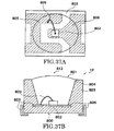
- Figs. 37A and 37B show such a typical conventional light emitting device.
- Fig. 37A is a plan view showing a configuration of the substantially part thereof, and
- Fig. 37B is a cross-sectional view thereof.
- the light emitting device shown here is of a so-called "surface mounting” type, including a package (resin stem) 800, semiconductor light emitting element 802 and sealing element 804 of a resin.
- the resin stem 800 has a structure molding a pair of leads 805, 806 shaped from lead frames with a resin portion 803 of a thermoplastic resin.
- the resin portion 803 has an opening 801, and the semiconductor light emitting element 802 is place therein. Then the semiconductor light emitting element 802 is sealed with an epoxy resin 804.
- the semiconductor light emitting element 802 is mounted on the lead 806.
- An electrode (not shown) of the semiconductor light emitting element 802 and the lead 805 are connected to each other by a wire 809.
- the semiconductor light emitting element 802 emits light, and the light is extracted from an emission surface 812 via the epoxy resin 804.
- the light emitting device shown in Figs. 37A and 37B certainly meets the requirements currently in force, i.e., 100 cycles as the current level of temperature cycle tests requested for ordinary civilian uses, and 300 cycles for car-borne uses. However, for further improvement of the reliability toward the future uses, essential review is required.
- the epoxy resins 804 is physically hard and fragile and produces a large stress upon hardening and that there still exists room for improvement in quality of close contact with the resin portion 803 of a thermoplastic resin that surrounds it.
- Those having two or more semiconductor elements different in emission wavelength can provide mixed color, thereby to diversify the color representation.
- two complementary colors can produce white light.
- the light emitting device shown in Figs. 37A and 37B cannot provide a sufficient space for mounting the chip and for bonding the wire as well. If two chips are packed in the narrow opening by force, the optical axis of the light emitting element will largely offset from the center of the opening, and the intensity profile of the emitted light, i.e., luminous intensity property, will become asymmetrical. Then, the light emitting device cannot provide a uniform emission pattern required in applications such as the back light of a liquid crystal display.
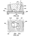
- Fig. 39 is a schematic diagram showing a plan-viewed configuration of a light emitting device prepared by the Inventor for trial toward the present invention.
- the light emitting device shown here has an approximately rectangular opening 901 formed in a resin portion 903, and chips 902A, 902B mounted on opposed leads 905, 906, respectively, at the bottom of the opening 901. Wires 909A, 909B extending from the chips 902A, 902B are connected to the opposed leads 906, 905, respectively.
- the fist problem is that a part of an adhesive extruding out upon mounting the chips 902A, 902B causes insufficient bonding of the wires 909A, 909B.
- pastes such as silver paste or solders such as gold-tin (AuSn) or gold-germanium (AuGe) solder is usually used.
- the second problem lies in that the illustrated rectangular shape of the opening 901 causes side walls of the resin portion 903 to be uniformly thin, and makes the mechanical strength insufficient. This problem becomes serious especially when a soft resin is used as the sealing element buried in the opening.
- a silicone resin used as the sealing element is advantageous for reducing the residual stress and thereby reducing cracks of the sealing element and breakage of the wire.
- the relatively soft silicone resin often fails to prevent an external lateral force to act on the chip and the wire. For example, upon picking up the light emitting device by grasping from its side surfaces for assembly and a test, the force actually acted upon the chip and the wire, and often deformed the wire.
- the third problem is that the illustrated rectangular shape of the opening 901 need a larger quantity of resin buried therein, and sometimes increases the resin stress.
- the resin filled in the opening 901 produces a stress upon curing, or thereafter upon an increase of decrease of the temperature.
- the degree of the stress depends on the buried quantity of the resin, and tends to increase as the buried quantity increases. Moreover, as already explained with reference to Fig. 38, epoxy resins exhibit a large stress.
- the sealing resin filled in the illustrated rectangular opening 901 produced a large stress, and is liable to cause exfoliation of the chips 902A, 902B, and deformation or breakage of the wires 909A, 909B.
- a light emitting device comprising: a resin portion having an opening, said opening having an approximately elliptical or elongate-circular opening shape; a first semiconductor light emitting element disposed inside said opening; a semiconductor element disposed inside said opening; and a silicons resin provided inside said opening to enclose said first semiconductor light emitting element and said semiconductor element, said silicone resin having a hardness not lower than 50 in JISA value.
- another light emitting device comprising: a lead; a resin portion embedding at least a part of said lead; a first semiconductor light emitting element mounted on said lead in an opening formed in said resin portion; a semiconductor element mounted on said lead in said opening; a wire connecting said first semiconductor light emitting element and said lead; and a silicone resin provided in said opening to enclose said first semiconductor light emitting element and said semiconductor element, said silicone resin having a hardness not lower than 50 in JISA. value, said lead having a slit formed therein between a portion where said first semiconductor light emitting element is mounted and a portion where said wire is connected.
- another light emitting device comprising: a first lead; a second lead; a resin portion embedding at least a part of said first and second leads; a first semiconductor light emitting element mounted on said first lead in an opening formed in said resin portion; a semiconductor element mounted on said second lead in said opening; a first wire connecting said first semiconductor light emitting element and said second lead; a second wire connecting said semiconductor element and said first lead; and a silicone resin provided in said opening to enclose said first semiconductor light emitting element and said semiconductor element, said silicone resin having a hardness not lower than 50 in JISA value, said first lead having a first slit formed therein between a portion where said first semiconductor light emitting element is mounted and a portion where said second wire is connected, said second lead having a second slit formed therein between a portion where said semiconductor element is mounted and a portion where said first wire is connected.
- another light emitting device comprising: a first lead;a second lead; a resin portion embedding at least a part of said first and second leads; a first semiconductor light emitting element mounted on said first lead in an opening formed in said resin portion; a semiconductor element mounted on said first lead in said opening; a first wire connecting said first semiconductor light emitting element and said second lead; a second wire connecting said semiconductor element and said second lead; and a silicone resin provided in said opening to enclose said first semiconductor light emitting element and said semiconductor element, said silicone resin having a hardness not lower than 50 in JISA value, said opening having a substantially elliptical or elongate-circular opening shape,said first semiconductor light emitting element and said semiconductor element being arranged along a longer axis or a shorter axis of said elliptical or elongate-circular opening.
- another light emitting device comprising: a semiconductor element; a first semiconductor light emitting element mounted on said semiconductor element by a metal bump; a silicone resin provided to enclose said semiconductor element and said first semiconductor light emitting element, said silicone resin having a hardness not lower than 50 in JISA value.
- another light emitting device comprising: a semiconductor light emitting element; a silicone resin provided to enclose said semiconductor light emitting element, said silicone resin having a hardness not lower than 50 in JISA value; and a fluorescent element which is included in said silicone resin, absorbs light emitted from said semiconductor light emitting element and releases light of a peak wavelength different from said light from said semiconductor light emitting element.
- the "elongate-circle” means a shape connecting a pair of curved portions by a pair of substantially straight portions.
- the curved portions may be either regularly arc-shaped or irregularly arc-shaped.
- silicon resin any resin having as its skeleton a structure in which silicon atoms having organic radicals such as alkyl radicals or aryl radicals are alternately connected to oxygen atoms. Needless to say, those containing additive elements added to such skeletons are also included in “silicone resins”.
- the "fluorescent element” may be any having a wavelength converting function, either inorganic or organic, including inorganic dyes having a wavelength converting function.
- a light emitting device using a silicone resin as the material of a sealing element and having a unique layout pattern of chips.
- Figs. 1A and 1B show schematic diagrams illustrating a configuration of the substantial part of a light emitting device according to the first embodiment of the invention, in which Fig. 1A is a plan view and Fig. 1B is a cross-sectional view taken along the A-A line of Fig. 1A.
- the light emitting device 1A shown here includes a resin stem 100, a semiconductor light emitting element 106A mounted on the resin stem 100, a protective Zener diode 106B and a sealing element 111 provided to embed them.
- the resin stem 100 includes leads 101, 102 shaped from a lead frame, and a resin portion 103 molded integrally with the leads 101, 102.
- the resin portion 103 is typically made of a thermoplastic resin preferably, for example, of a nylon system having inert coupling radicals.
- the thermoplastic resin may be a resin having a high resistance to heat, such as liquid crystal polymer (LCP), polyphenylene sulfide (PPS: thermoplastic resin) or syndiotactic polystyrene (SPS: crystalline polystyrene).
- LCP liquid crystal polymer
- PPS polyphenylene sulfide
- SPS syndiotactic polystyrene
- the plan-viewed outer configuration of the resin portion 103 may be a substantial square approximately sized 2.0 ⁇ 2.0mm through 6.0 ⁇ 6.0mm, or a substantial rectangular approximately sized 2.0 ⁇ 3.0mm through 5.0 ⁇ 7.0mm.
- the leads 101, 102 have opposed ends close to each other, and extend therefrom in the opposite directions to outside the resin portion 103.
- the resin portion 103 has formed an opening 105, and the semiconductor light emitting element 106A and the diode 106B are mounted at the bottom of the opening 105.
- the plan-viewed shape of the opening 105 is approximately elliptical or approximately elongate-circular as illustrated.
- the inner wall surface of the resin portion 103 surrounding the elements 106A, 106B inclines to face toward the light extraction direction to function as a reflective surface 104 for reflecting light.
- the light emitting device shown in Figs. 1A and 1B is characterized in (1) the material of the sealing element 111, (2) shape of the opening 105 and (3) layout of the leads and the chips in the opening 105.
- the material of the sealing element 111 is explained below in greater detail.
- the invention uses a silicone resin instead of a conventional epoxy resin as the sealing element 111 filling the opening 105.
- silicone resins are less fragile and less subjected to cracks.
- Silicone resins usable in the present invention exhibit a high bonding force with the resin portion 103 made of a thermoplastic resin, for example, and a high moisture resistance. Additionally, they do not crack or exfoliate so much due to a temperature stress. Furthermore, such a silicone resin filled in the opening produces only a remarkably small resin stress to the light emitting element 106A and the Au wire 109.
- silicone resins are more resistance to light irradiated from the light emitting element 106A than epoxy resins.
- Rubber-like silicone resins have a JISA hardness in the range of approximately 50 to 90.
- Epoxy resins widely used as the sealing element materials in conventional light emitting devices have a JISA hardness around 95.
- rubber-like silicone resins having a JISA hardness in the range of 50 to 90 are prevented from deformation by a selector or an assembler used for selecting or assembling light emitting devices.
- a technique for increasing the hardness of a silicone resin is to add an agent for giving a thixotropy index.
- a silicone resin Upon burying a silicone resin, it is poured into the opening 105 of the resin stem through a thin nozzle, and thereafter cured. In this process, it is preferable to use a silicone resin having a pre-curing viscosity around 100cp through 10000cp. Thereby, it is possible to fully bury the opening including narrow spaces and to limit the residual stress upon curing within a sufficiently low range, without giving an excessive stress to the light emitting element 106A (diode 109B) and the wire 109A (109B).
- the Inventor prepared light emitting devices according to the embodiment as shown in Figs. 1A and 1B by using a rubber-like silicone resin having the pre-during viscosity of 1000cp and post-curing JISA hardness value of 70, and carried out a temperature cycle test in the temperature range from -40°C to 110°C.
- a temperature cycle test in the temperature range from -40°C to 110°C.
- the inventor also prepared light emitting devices using epoxy resins, and carried similar evaluation. As a result, epoxy resins cracked near 700 cycles. In this manner, the devices using silicone resins have been confirmed to be greatly improved in reliability as compared to those using epoxy resins.
- the Inventor also carried out quantitative analysis of the stress applied to the semiconductor light emitting element with devices using silicone resins and devices using epoxy resins, respectively.
- Light emitting devices taken for the analysis were prepared by forming a 0.9 mm deep, 2.4 mm diameter, circular opening in the resin portion 103 of the package, mounting a semiconductor light emitting element 106 at the bottom of the opening, and burying a silicone resin of the JISA hardness of 70.
- Devices as comparative examples were prepared by burying an epoxy resin in the similar structure. In both types of light emitting devices, the semiconductor light emitting element had the size of 200 ⁇ 200 ⁇ m and the thickness of 150 ⁇ m.
- the temperature of 240°C is the peak temperature that may be applied when the light emitting device is fixed to a packaging substrate, for example, by reflow of a solder. As shown, when the light emitting device is heated, a stress corresponding to the thermal expansion of the resin is applied to the light emitting element.
- the stress level of 3.5 ⁇ 10 -6 produced in the epoxy resin is the level where breakage of wire will occur before 1000 cycles approximately in the temperature cycle test in the temperature range of -40°C to 110°C, according to the statistics of the reliability test carried out by the Inventor.
- the stress applied to the light emitting element is about a half the stress given by the epoxy resin.
- Such a small stress is assumed to be the reason of realizing the remarkably high reliability by eliminating cracks of the resin, exfoliation of the light emitting element, deformation or breakage of wires, and absolutely eliminating malfunctions even in the temperature cycle of 1500 cycles.
- a silicone resin in particular, a rubber-like silicone resin, reduces the possibility of cracks and exfoliation that often occurred in conventional epoxy resins, breakage of wires, and so on.
- silicone resin also improves the durability against light emitted from the semiconductor light emitting element 106 or light intruding from the exterior of the light emitting device. Epoxy resins change in color when exposed to light, and even if it is initially transparent, its optical transmittance decreases after long-time use.
- silicone resin leads to a very satisfactory result. That is, if a silicone resin is used, change or color and other types of deterioration do not occur even after it is exposed to short wavelength light such as ultraviolet rays. Therefore, silicone resins contribute to realization of light emitting devices exhibiting excellent resistance to light and weather.
- the resin portion 103 may be equipped with optical reflectivity.
- the resin portion 103 may be made of 65 or more weight % of a thermoplastic resin and 35 or less weight % of a filling agent.
- the filling agent contains a high-reflective material such as titanium oxide (TiO 3 ), silicon oxide, aluminum oxide, silica or alumina. In case of titanium oxide, its content is in the range from 10 to 15%.
- TiO 3 titanium oxide
- the reflective surface 104 is a part of the resin portion containing a diffusing material that reflects light, it can reflect light from the light emitting element 106 and the fluorescent element 110 upward to realize a high luminance of the light emitting device. If the reflective surface 104 is configured as a paraboloid of revolution, for example, the output and the quality of the light emitting device can be further improved.
- the sealing element 111 of a silicone resin may also contain such a diffusing material diffused therein to expand the luminous distribution property broader.
- the opening 105 is approximately elliptical.
- the lead 101 and the lead 102 are isolated. Near the distal end of the lead 101, a slit 101G is formed to divide it into the regions 101A and 101B. similarly, near the distal end of the lead 102, a slit 102G is formed to divide it into the regions 102A and 102B.
- the light emitting element 106A is mounted in the region 101A with an adhesive such as silver (Ag) paste.
- the light emitting element 106B is mounted in the region 102B similarly with an adhesive 107 such as silver (Ag) paste.
- the wire 109A is connected to the opposed region 102A. From an electrode (not shown) formed on the diode 106B, the wire 109B is connected to the opposed region 101B.
- the slits 101G, 102G formed near distal ends of the leads 101, 102 separate each of them into the portion (101A, 102B) for mounting the chips 106A, 106B and the portion (101B, 102A) for bonding the wires 109A, 109B.
- This configuration keeps the portion for bonding the wire clean even when silver paste, for example, extrudes upon mounting the chip, and thereby eliminates defective bonding of wires.
- the invention employs a shape with a longer diameter and a shorter diameter such as an approximately elliptical shape or an approximately elongate-circular shape as the shape of the opening in lieu of an approximately circular shape as shown by a broken line in Fig. 1A, which has been used conventionally, it is possible to effectively increase the area of the opening 105 and thereby make an ample space for mounting two or more chips and bonding the wires.
- the approximately elliptical or elongate-circular shape of the opening according to the invention makes it easy to locate the light emitting element closest to the center of the opening.
- the use of the approximately elliptical or elongate-circular shape of the opening according to the invention also enables the corner portions 103C to be made thicker. As a result, the light emitting device maintains a sufficient mechanical strength, and it is prevented from deformation or wires and other kinds of damage even upon application of a lateral force during assembly or tests.
- the approximately elliptical or elongate-circular shape of the opening prevents an increase of the resin quantity filled inside and thereby prevents the resin stress.
- the resin stress increases as the quantity of resin filled as the sealing element 111 increases.
- the invention minimizes the increase of the resin quantity and simultaneously keeps an ample space for locating a plurality of chips. It results in eliminating the problems of exfoliation of chips, deformation or breakage of wires due to an increase of the resin stress. This effect is obtained as an additional effect by the use of a silicone resin as the sealing element 111.
- the invention enables mounting of a plurality of chips while maintaining the outer dimension of the light emitting device compact. Therefore, by connecting the protective diode 106B in a parallel, opposite direction from the light emitting element 106A as illustrated, the invention can improve the reliability. In addition, by combining light emitting elements different in emission wavelength, the device can realize emission of white and other various colors, which has been difficult to emit conventionally.
- the slits 101G, 102G formed in the leads 101, 102 facilitate corners of the lead patterns to be cognized inside the opening in the process of mounting chips or bonding wires. Therefore, the invention ensures more accurate mounting positions of the chips and more accurate bonding positions of the wires than conventional techniques.
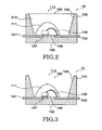
- Fig. 2 is a cross-sectional view that schematically shows the second specific example regarding a sealing element 111 in the light emitting device according to the first embodiment.
- Figs. 1A and 1B are commonly labeled, and their detailed explanation is omitted for simplicity.
- the light emitting device 1B shown here also includes a resin stem 100, semiconductor light emitting element 106 mounted thereon, and sealing element 111 of a silicone resin provided to embed the element 106.
- the sealing element 111 merely embeds the light emitting element 106, and a second sealing element 213 of a transparent resin is provided outside the sealing element 111.
- the second sealing element 213 may be made of an epoxy resin, silicone resin or any of other various materials.
- the second sealing element 213 may be colored, and any material adaptable to the dye or coloring agent used can be selected.
- the second sealing element 213 may contain a diffusing material dispersed therein to scatter light. In this case, light can be diffused, and broader light distribution characteristics can be obtained.
- a silicone resin is used as the second sealing element 213, then its close contact with the sealing element 111 is enhanced, and the moisture resistance is improved.
- the sealing element 111 made of a silicone resin wraps the entirety of the Au wire 109. Therefore, a reliable light emitting element free from breakage of wire due to a resin stress can be realized. If the wire partly projects into the second sealing element 213, it will readily break due to a stress produced at the interface between the sealing elements 111, 213. In this specific example, however, since the wire 109 is entirely embedded by the sealing element 111, it is free from breakage.
- Fig. 3 is a cross-sectional view that schematically shows the third specific example regarding the sealing element 111 in the light emitting device according to the first embodiment.
- the same or equivalent components as those already explained with reference to Figs. 1A, 1B and 2 are commonly labeled, and their detailed explanation is omitted for simplicity.
- the light emitting device 1C shown here also includes a resin stem 100, semiconductor light emitting element 106 mounted thereon, and sealing element 111 provided to embed the element 106.
- the sealing element 111 merely embeds the light emitting element 106. In this specific example, however, the space outside the sealing element 111 remains open, without being filled by any other sealing element.
- the limitative use of the sealing element 111 only to enclose the light emitting element 106 mounted at the bottom of the opening 105 contributes to small-sizing the emitting portion. Therefore, the luminance increases, and the function of the reflective surface 104 to gather rays of light is enhanced.
- the approximately hemispheric sealing element 111 serves as the emission point, and the reflective surface 104 surrounds it, the same optically converging effect as a conventional lamp can be obtained.
- the sealing element 111 embeds the entirety of the Au wires 108, 109, it prevents breakage of wire by a resin stress, and ensures a high reliability.
- Fig. 4 is a cross-sectional view that schematically shows the fourth specific example regarding the sealing element 111 in the light emitting device according to the first embodiment.
- the light emitting device 1D shown here also includes a resin stem 100, semiconductor light emitting element 106 mounted thereon, and sealing element 111 embedding the element 106.
- the embodiment shown here includes a convex transparent element 413 is provided on the sealing element 111 to ensure the function of gathering rays of light.
- the transparent element 413 may be made of a resin, for example.
- a silicone resin is advantageous for decreasing the difference of the refractive index from the sealing element 111 and to reduce the loss by reflection at the interface with the sealing element 111.
- the convex shape of the transparent element 413 is not limited to a spherical shape. Any appropriate shape can be selected depending on the required converging ratio or luminous intensity profile.
- Fig. 5 is a plan view that schematically shows the fifth specific example regarding the sealing element 111 in the light emitting device according to the first embodiment.
- the same or equivalent components as those already explained with reference to Figs. 1A through 4 are commonly labeled, and their detailed explanation is omitted for simplicity.
- the light emitting device shown here includes two semiconductor light emitting elements 106, 106C on board.
- elements 106A, 106C reversed in conduction type may be used. That is, one of them may be configured n-side down while the other p-side down.
- the optical output of the light emitting device can be doubled.
- the light emitting device can provide light of a mixed color.
- white light can be realized by combining, for example, a blue light emitting element and a yellow light emitting element that are chromatically complementary.
- White light can be obtained also by combining a red light emitting element and a blue-green light emitting element.
- Fig. 6 is a cross-sectional view that schematically shows the structure of a semiconductor light emitting element usable in the configuration shown in Figs. 1A and 1B or Fig. 5. This structure is briefly explained here.
- the light emitting element 106A (or 106C) includes a buffer layer 122, n-type contact layer 123, light emitting layer 124, p-type cladding layer 125 and p-type contact layer 126 sequentially stacked on a conductive substrate 121.
- the light emitting layer 124 may have a quantum well (QW) structure in which barrier layers and well layers are stacked alternately.
- QW quantum well
- the conductive substrate 121 may be made of, for example, an n-type semiconductor. Respective layers on the substrate may be made of, for example, III-V compound semiconductors, II-IV compound semiconductors, IV-VI compound semiconductors and other various materials.
- n-side electrode 127 is provided on the rear surface of the substrate 121.
- Surface of the element is covered by a protective film 130 of SiO 2 .
- the emission wavelength can be adjusted in a wide range by adjusting the material and thickness of the light emitting layer.
- the embodiment shown here can realize various emission colors by using such semiconductor light emitting elements.
- Fig. 7 is a plan view that schematically shows the sixth specific example according to the first embodiment.
- the same or equivalent components as those already explained with reference to Figs. 1A through 5 are commonly labeled, and their detailed explanation is omitted for simplicity.
- the light emitting device shown here includes a protective diode 106B and a semiconductor light emitting element 106D.
- the light emitting element 106D is formed on an insulating substrate, and includes p-side and n-side electrodes (not shown) on the front surface. Wires 109B, 109C extending from these electrodes are connected to the leads 101B, 102B, respectively.
- the protective diode 106B and the light emitting element 106D are connected in the opposite directions in parallel.
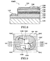
- Fig. 8 is a cross-sectional view that shows a structure of the semiconductor light emitting element 106D.
- the device shown here is made by stacking semiconductor layers on an insulating substrate 133. More specifically, sequentially stacked on the insulating substrate 133 are a buffer layer 122, n-type contact layer 123, light emitting layer 124, p-type cladding layer 125 and p-type contact layer 126.
- the light emitting layer 124 may have a quantum well (QW) structure in which barrier layers and well layers are stacked alternately.
- QW quantum well
- an n-side electrode 127 is formed on the n-type contact layer 123 exposed by selectively removing the multi-layered structure from its surface by etching.
- an n-side electrode 127 is formed on the p-type contact layer 126 .
- Surface of the element is covered by a protective film 130 of SiO 2 .
- the specific example shown in Fig. 7 can compactly accommodate both the semiconductor light emitting element 106D formed on the insulating substrate and the protective diode 106B in a limited space, and can reliably, easily bond the predetermined wires 109A through 109C. Moreover, since the chips and the wire bonding portion are isolated by the slits 101G, 102G, defective bonding by extrusion of the adhesive can be eliminated.
- Fig. 9 is a plan view that schematically shows the seventh specific example according to the first embodiment.
- the same or equivalent components as those already explained with reference to Figs. 1A through 7 are commonly labeled, and their detailed explanation is omitted for simplicity.
- the light emitting device shown here also includes the protective diode 106B and the semiconductor light emitting element 106D.
- the opening 105 is not elliptical but approximately elongate-circular.
- the "elongate circle” means a shape, like that of the opening 105 shown in Fig. 9, having a pair of opposed approximately arc-curved portions and connecting these curved portions by substantially straight portions.
- the curved portions need not be strictly arc-shaped. That is, the "approximately elongate-circle" pertains to a shape made up of a pair of curved portions connected by two substantially straight portions.
- the approximately elongate circle is advantageous for easier processing upon forming the opening 105 in the resin portion 103.
- the light emitting device can maintain a sufficient mechanical strength against a lateral stress or impulse.
- shapes of the distal ends of the pair of leads 101, 102 are asymmetric. That is, the portion 102B for mounting the light emitting element 106D on is formed to extend forward toward the center of the opening 105.
- the light emitting element 106D can be located in the center of the opening 105, and the intensity profile of the emitted light, i.e. the luminous intensity property can be approximated to a uniform or symmetric profile. It is also possible to enhance the luminance.
- “Locating in the center” herein means to locate any portion of the light emitting element 106D on the central axis of the opening 105.
- the specific example shown here may use the light emitting element 106A (or 106C) using a conductive substrate as shown in fig. 6 instead of the light emitting element 106D.
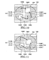
- Fig. 10 is a plan view that schematically shows the eighth specific example according to the first embodiment.
- the same or equivalent components as those already explained with reference to Figs. 1A through 9 are commonly labeled, and their detailed explanation is omitted for simplicity.
- the light emitting device shown here also includes the protective diode 106B and the semiconductor light emitting element 106D.
- the opposed distal ends of the pair of leads 101, 102 are aligned straight instead of being offset. Then the diode 106B and the light emitting element 106D are mounted at diagonal positions.
- the light emitting element 106D is formed to be closer to the center of the opening 105 than the diode 106B. Locating the optical axis closer to the center of the opening 105 ensures a more uniform luminous intensity property.
- Fig. 11 is a plan view that schematically shows the ninth specific example according to the first embodiment.
- the same or equivalent components as those already explained with reference to Figs. 1A through 10 are commonly labeled, and their detailed explanation is omitted for simplicity.
- the light emitting device shown here also includes the protective diode 106B and the semiconductor light emitting element 106D, and the opposed distal ends of the pair of leads 101, 102 are aligned straight instead of being offset.
- the slits 101G, 102G are formed to be offset from each other. This configuration can also locate the light emitting element 106D close to the center of the opening 105.
- Fig. 12 is a plan view that schematically shows the tenth specific example according to the first embodiment.
- the same or equivalent components as those already explained with reference to Figs. 1A through 11 are commonly labeled, and their detailed explanation is omitted for simplicity.
- two chips are mounted on a common lead, and they are aligned along the lengthwise direction of the opening 105 having an approximately elliptical or elongate-circular shape.
- the semiconductor light emitting elements 106A, 106C are mounted side by side on the lead 101, and the wires 109A, 109B are connected to the lead 102 in the opposed position with respect to the shorter axis of the opening 105.
- This arrangement of a plurality of chips along the longer axis, i.e. length wise direction, of the approximately elliptical or elongate-circular opening 105 is advantageous for effective use of the limited space.
- Fig. 13 is a plan view that schematically shows the eleventh specific example according to the first embodiment.
- the same or equivalent components as those already explained with reference to Figs. 1A through 12 are commonly labeled, and their detailed explanation is omitted for simplicity.
- a second wire 109C from the light emitting element 106D formed on the insulating substrate it is necessary to connect a second wire 109C from the light emitting element 106D formed on the insulating substrate to the lead 101.
- a slit 101G is formed in the lead 101, and the wire 109C is connected across the slit 101G. In this manner, the bonding region can be isolated from extrusion of the adhesive upon mounting the light emitting element 106D and the diode 106B.
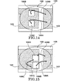
- Fig. 14 is a plan view that schematically shows the twelfth specific example according to the first embodiment.
- the same or equivalent components as those already explained with reference to Figs. 1A through 13 are commonly labeled, and their detailed explanation is omitted for simplicity.
- two chips are mounted on a common lead. These two chips, however, are disposed along the shorter axis direction of the approximately elliptical or elongate-circular opening 15. Then the wires 109A, 109B are connected to the lead 102 in the opposed position with respect to the shorter axis of the opening 105.
- This arrangement of a plurality of chips along the shorter axis of the approximately elliptical or elongate-circular opening 105 is also advantageous for effective use of the limited space.
- Fig. 15 is a plan view that schematically shows the thirteenth specific example according to the first embodiment.
- the same or equivalent components as those already explained with reference to Figs. 1A through 14 are commonly labeled, and their detailed explanation is omitted for simplicity.
- a second wire 109C from the light emitting element 106D it is necessary to connect a second wire 109C from the light emitting element 106D to the lead 101.
- a slit 101G is formed in the lead 101, and the wire 109C is connected across the slit 101G. In this manner, the bonding region can be isolated from extrusion of the adhesive upon mounting the light emitting element 106D and the diode 106B.
- Fig. 16 is a plan view that schematically shows the fourteenth specific example according to the first embodiment.
- the same or equivalent components as those already explained with reference to Figs. 1A through 15 are commonly labeled, and their detailed explanation is omitted for simplicity.
- a slit 101G is formed in the lead 101 to divide its distal end into two parts 101A, 101B.
- the distal end of the lead 102 is divided into parts 102A, 102B. These divisional parts extend into the opening 105.
- the light emitting element 106D and the protective diode 106B are disposed on the divisional part 101A of the lead 101 along the longer axis of the opening 105.
- a wire 109A extending from the diode 106B is connected to the divisional part 102B of the lead 102.
- a wire 109B from the light emitting element 106D is connected to the divisional part 102A of the lead 102, and the a wire 109C from the light emitting element 106D is connected to the divisional part 101B of the lead 101 across the slit 101G.
- the chip layout in the specific example shown here makes it possible to locate the light emitting element 106D in the center of the opening 105. Additionally, the mode of connecting the wire 109C across the slit 101G can isolate and protect the bonding region of the wire 109C from extrusion of the adhesive upon mounting the diode 106B and the light emitting element 106D.
- Fig. 17 is a cross-sectional view that schematically shows a configuration of the substantial part of a light emitting device according to the second embodiment of the invention.
- the same or equivalent components as those already explained with reference to Figs. 1A through 16 are commonly labeled, and their detailed explanation is omitted for simplicity.
- a semiconductor light emitting element 106F overlies a protective zener diode 106E. That is, the diode 106E is mounted on the lead 101, and the light emitting element 106F is mounted thereon by flip-chip mounting. Then a wire 109 extends from the diode 106E, and it is connected to the lead 102.
- the sealing element 111 is preferably made of a silicone resin having a JISA hardness in the range from 50 to 90 to ensure various advantages including reliability as already explained with reference to the first embodiment.
- Fig. 18A is a cross-sectional view that shows a chip portion of the light emitting device according to the second embodiment in an enlarged scale.
- the protective diode 106E has a planar structure in which a p-type region 152 is formed on the top surface of an n-type silicon substrate 150.
- the p-side electrode 154 is formed in the p-type region 152, and the n-side electrode 156 is formed on the bottom surface of the substrate 150.
- another n-side electrode 158 is formed on the top surface of the diode, and a wiring layer 160 connecting the upper and lower n-side electrodes 156, 158 is formed to extend on a side surface of the diode 16E.
- a high-reflectance film 162 is formed on the top surface of the diode 106E.
- the high-reflectance film 162 has a high reflectance against light emitted from the light emitting element 106F. It may be, for example, a metal film, or a Bragg reflection film stacking two or more kinds of thin films different in refractive index.
- the semiconductor light emitting element 106F includes a buffer layer 122, n-type contact layer 123, n-type cladding layer 132, active layer (light emitting layer) 124, p-type cladding layer 125 and p-type contact layer 126 sequentially stacked on a translucent substrate 138 (illustrated upside down in Fig. 18A), and also includes an n-side electrode 127 and a p-side electrode 128. Light emitted from the active layer 124 passes through the translucent substrate 138, and extracted upward as illustrated.
- respective electrodes are connected to the electrode of the diode 106E by bump contacts 142, 144 that may be made of, for example, gold (Au) or indium (In).
- a wire 109 is bonded to the p-side electrode 154 of the diode 106E and connected to the lead 102.
- Fig. 18B is a circuit diagram of an equivalent circuit of the light emitting device.
- the instant embodiment vertically stacking the protective diode 106E and the light emitting element 106F can locate them in a very narrow space. Therefore, the outer dimension of the light emitting device need not be enlarged, and the conventional resin stem (package) as shown in Figs. 37A and 37B can be use directly.
- the use of the high-reflectance film 162 on the top surface of the diode 106E is effective for reflecting the light from the light emitting element 106F toward the direction for extraction and thereby improving the light extraction efficiency. Simultaneously, the high-reflectance film 162 removes the problem that the operation of the diode 106E is adversely affected or deteriorated by the light from the light emitting element 106F. Furthermore, the use of the high-reflectance film 162 prevents deterioration of the paste 107 coated under the diode 106E by light.
- the embodiment shown here can connect the chips to the lead with only one wire. As a result, it minimizes the problems caused by deformation or breakage of wire, and thereby improves the reliability.
- the embodiment shown here can provide the bump contact 142 with a high thermal conductivity close to the light emitting layer 124 of the light emitting element 106F to provide a heat radiation path via the wire layer 160. That is, it enhances the heat radiation efficiency of the light emitting element 106F, and thereby realizes a light emitting device operative under a wider temperature range and having a long-time reliability.
- the site of the high-reflectance film 162 is not limited to the top surface of the diode 106E, but the bottom surface of the light emitting element 106F is also acceptable.
- the high-reflectance film 162 may be inserted between the diode 106E and the light emitting element 106F.
- the multi-layered structure of the diode 106E and the light emitting 106F in the opening 105 results in thinning the sealing element 111 so much. There rises the possibility of insufficient strength of the sealing element 11 in the upper part of the chip or a high resin stress. As a result, if a conventional epoxy resin is used, there may occur cracks in an upper part of the chip or exfoliation or splitting of the chip as shown in Fig. 38.
- the invention can prevent cracks of the resin and reduce the resin stress by using a silicone resin as the sealing element 111.
- Fig. 19 is a cross-sectional view that schematically shows the second specific example regarding the sealing element 111 in the light emitting device according to the second embodiment.
- the same or equivalent components as those already explained with reference to Figs. 1A through 18 are commonly labeled, and their detailed explanation is omitted for simplicity.
- the sealing element 111 of a silicone resin having a JISA hardness in the range from 50 to 90 merely enclose the multi-layered structure of the diode 106E and the light emitting element 106F, and a second sealing element 213 made of a translucent resin is provided outside the sealing element 111.
- This configuration increases the freedom regarding the material and the additive material of the second sealing element 213 while maintaining a high reliability as already explained with reference to Fig. 2.
- Fig. 20 is a cross-sectional view that schematically shows a third specific example regarding the sealing element of the light emitting device according to the second embodiment.
- the same or equivalent components as those already explained with reference to Figs. 1A through 19 are commonly labeled, and their detailed explanation is omitted for simplicity.
- the sealing element 111 of a silicone resin having a JISA hardness in the range from 50 to 90 merely enclose the multi-layered structure of the diode 106E and the light emitting element 106F, the outside thereof is open without any other sealing element.
- This configuration downsizes the emission portion as already explained with reference to Fig. 3, thereby enhances the luminance, and enhances the light converging function of the reflective surface 104 as much as the light converging function of a conventional lamp.
- Fig. 21 is a cross-sectional view that schematically shows a fourth specific example of the light emitting device according to the second embodiment.
- the same or equivalent components as those already explained with reference to Figs. 1A through 20 are commonly labeled, and their detailed explanation is omitted for simplicity.
- a convex translucent element 413 is provided on the sealing element 111 of a silicone resin having the JISA hardness in the range from 50 to 90.
- the convex translucent element 413 functions to converge light.
- the translucent element 413 may be made of, for example, a resin.
- a silicone resin is especially advantageous for reducing the difference in refractive index from the sealing element 111 and to reduce the loss by reflection at the interface with the sealing element 111.
- the convex shape of the translucent element 413 is not limited to a hemisphere. Any other appropriate shape may be selected depending on the converging ratio or luminous intensity profile requested.
- the second embodiment can locate the light emitting element 106F in the center of the opening 105, the optical converging function of the convex translucent element 413 is maximized.
- a light emitting device as the third embodiment that is based on the light emitting device according to the first or second embodiment but mixes a fluorescent element in the sealing element 111 such that the light from the light emitting element can be extracted after wavelength conversion by the fluorescent element.
- Fig. 22 is a cross-sectional view that schematically shows a configuration of the substantial part of the light emitting device according to the third embodiment of the invention.
- the same or equivalent components as those already explained with reference to Figs. 1A through 21 are commonly labeled, and their detailed explanation is omitted for simplicity.
- the light emitting device shown here has a general configuration similar to that shown in Figs. 1A and 1B.
- the sealing element 111 filled in the opening 105 contains the fluorescent element 110 that absorbs primary light emitted from the light emitting element 106 and releases secondary light after wavelength conversion.
- Material of the fluorescent element 110 may be determined adequately taking account of the wavelength of the primary light emitted from the light emitting element 106, wavelength of the secondary light requested, and so on.
- the fluorescent element 110 may be designed either to convert the wavelength of a part of the primary light from the light emitting element 106 into secondary light so as to permit mixed light of the non-converted primary light and the secondary light to be extracted, or to absorb all of the primary light from the light emitting element 106 such that the secondary light alone is extracted substantially.
- the light emitting element 106 emits blue light
- fluorescent element converts the wavelength of a part of the blue light into yellow light
- white light as a result of mixture of the blue light and yellow light is extracted.
- the primary light and the secondary light may be complementary.
- this method can remove the problem of change of color by deviation or fluctuation of the emission characteristics of the light emitting element 106 and the fluorescent element 110. For example, even when the wavelength of the light emitting element 106 fluctuates among products or shifts due to various factors such as temperature conditions and changes with time, influences thereof to each fluorescent element are small, and the balance of the mixed color obtained from the fluorescent elements does not change substantially. It results in realizing a light emitting device having remarkably stable l ⁇ emission characteristics over a wide temperature range and a long operation time.
- the fluorescent element 110 may be either a singular material or a combination of a fluorescent element 110A for releasing red light, fluorescent element 110B for releasing green light and fluorescent element 110C for releasing blue light. In this case, white color is obtained. There are, however, various other combinations as explained later.
- Fluorescent elements 110 and sealing elements 111 usable in the third embodiment will be explained below in greater detail.
- the fluorescent element 110 used in the embodiment of the invention is a fluorescent material that releases light by absorbing ultraviolet light shorter than 400 nm emitted from the light emitting layer 124 of the light emitting element 106, or a material that releases light by absorbing light emitted from another fluorescent element.
- the fluorescent element 110 preferably has a conversion efficiency of 1 lumen/watt or more.
- White light can be realized by mixing three primary colors of red, green and blue, or by mixing any two complementary colors.
- white light by three primary colors can be realized by using a first fluorescent element for releasing blue light by absorbing the primary light from the light emitting element 106, a second fluorescent element for releasing red light, and a third fluorescent element for releasing green light.
- white light can be realized by using a light emitting element 106 which emits blue light, a first fluorescent element which releases red light by absorbing the primary light from the light emitting element, and a second fluorescent element which releases green light by absorbing the primary light from the light emitting element, and by mixing these primary light and secondary lights.
- White light by complementary colors can be realized by combining a first fluorescent element for releasing blue light by absorbing light from the light emitting element 106 and a second fluorescent element for emitting yellow light by absorbing the blue light, or by combining a first fluorescent element for releasing green light by absorbing light from the light emitting element 106 and a second fluorescent element for releasing red light by absorbing the green light.
- Fluorescent elements whose wavelength changes are not larger than 50 nm in the temperature range from -40°C to 100°C are preferably used to realize a light emitting device independent from temperature characteristics of the light emitting element.
- the use of fluorescent elements whose wavelength changes do not exceed 50 nm when the light emitting element 106 is operated by a drive current in the range from 1mA to 100mA enables realization of a light emitting device independent from changes in emission spectrum caused by the drive current of the element.
- the following fluorescent material for example, can be used for releasing yellow light.
- any desired tone can be made.
- white colors from white lamp color to white fluorescent lamp color can be realized by one of 1:1:1 through 7:1:1, 1:1:1 through 1:3:1 and 1:1:1 through 1:1:3 in R:G:B weight % ratio.
- the tone of the sealing element 111 will become white. That is, since the light emitting device emitting white light looks white also in the OFF state, its appearance is good, and a light emitting device excellent from the visual and design viewpoints can be provided.
- Fluorescent materials usable in the invention are not limited to inorganic fluorescent materials. High-luminance light emitting devices can be realized also by similarly using the following organic dye materials.
- individual dye materials can be dispersed in the resin by adding respective dye materials into a silicone resin as the sealing element and stirring it, and excitation efficiency of dyes can be enhanced.
- various colors of light can be realized with the light emitting device by combining appropriate materials of the fluorescent element (including dyes) 110 contained in the sealing element 111. That is, any desired tone can be realized by combining red, green, blue and yellow fluorescent materials (and dyes).
- the embodiment of the invention can also realize stabilization of the emission wavelength, which could not attained with conventional semiconductor light emitting elements, even by using a single fluorescent element. That is, ordinary semiconductor light emitting elements are subject to shifting of the emission wavelength depending on the drive current, ambient temperature and modulating conditions. In contrast, in the light emitting device according to the embodiment of the invention, the emission wavelength is remarkably stable, independently of changes of the drive current and temperature by substantially extracting only the secondary lights emitted from the fluorescent elements.
- the emission characteristics of the light emitting device according to the embodiment of the invention is determined by the characteristics of the additive fluorescent element 110 regardless of characteristics of the light emitting element 106, the production yield can be increased without variances of characteristics among different light emitting devices.
- the Inventors have got new knowledge about the surface configuration of the sealing element 111 through his own trial and review about it.
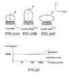
- Figs. 23A through 23C show schematic diagrams that illustrate intensity profiles of emitted light depending upon the surface configuration of the sealing element.
- the profile of Fig. 23A is the intensity profile P of light from the light emitting element 106 using a sealing element 111 having a flat surface configuration
- the profile of Fig. 23B is that with a sealing element 111 having a concave surface configuration
- the profile of Fig. 23C is that with a sealing element 111 having a convex surface configuration.
- the intensity profile, i.e. orientation characteristics, of the emitted light of the device having the concave surface configuration shown in fig. 23B apparently converges in the direction of the vertical axis Z.
- the profile corresponding to the convex surface configuration shown in Fig. 23C diverges in the direction of the xy plane.
- the light emitted from the fluorescent element contained near the convex portion of the sealing element 111 having the convex surface configuration spreads in the xy plane direction whereas the light emitted from the fluorescent element contained near the surface of the sealing element having the concave surface configuration is reflected by the side wall reflective surface 104 and contributes to increase the ratio of light traveling in the z-axis direction.
- the surface configuration of the sealing element 111 can be determined by adjusting its quantity to be buried. That is, by adjusting the filling quantity of the sealing element 111, any desired orientation characteristics of the emitted light can be obtained.
- the convex surface configuration of the sealing element 111 may generate undesirable excited light in receipt of the light from adjacent light emitting devices. Therefore, the sealing element 111 preferably has a concave surface configuration also in applications of this kind.
- the embodiment of the invention can reliably, readily cope with those requirements by adjustment of the filling quantity of the sealing element 111.
- the sealing element 111 is a member containing the fluorescent element 110 buried in the opening 105 to convert primary light from the light emitting element 106.
- the sealing element 111 is preferably made of a material having a larger coupling energy than the energy of the primary light from the light emitting element 106. Additionally, it preferably has the property of transmitting light after wavelength conversion by the fluorescent element 110.
- the optical resistance to the primary light emitted from the light emitting element 106 may not be sufficiently high. More specifically, in receipt of primary light from the light emitting element 106, epoxy resins, originally transparent, change in color through yellow, liver to black, and it results in a serious decrease of the light extraction efficiency. This problem becomes more serious as the wavelength of the primary light becomes shorter.
- silicone resin leads to a very satisfactory result. That is, if a silicone resin is used, change or color and other types of deterioration do not occur even after it is exposed to light having a comparatively shorter peak wavelength. By actually using silicone resin in a light emitting device using short-wavelength light as primary light, a high reliability could be realized.
- silicone resins have a fairly high transmittance in the wavelength range from ultra violet through the visible range.
- the optical transmittance thereof can be kept more than 60% of the initial value even after operation of 1000 hours.
- silicone resin containing the fluorescent element 110 is coated onto the light emitting element 106 mounted in the opening 105 by supplying it through a narrow nozzle while agitating it to uniformly mix predetermined fluorescent materials, and it is thereafter hardened.
- a silicone resin having a pre-curing viscosity around 100cp through 10000cp because it can hold particles of the fluorescent element uniformly dispersed without segregation or segmentation. In this manner, light from the excited fluorescent element is uniformly, adequately spread by a fluorescent element having a large refractive index without being excessively spread or absorbed by other fluorescent elements. Therefore, light is uniformly mixed, and tone irregularity can be prevented.
- the silicone resin used in the embodiment of the invention has a high bonding force to the resin portion 103 and a high strength to humidity, and it is unlikely to crack even under a temperature stress. Additionally, the silicone resin buried in the opening can greatly alleviate the resin stress to the light emitting element 106 and the Au wire even upon changes of the ambient temperature.
- Rubber-like silicone resins have a JISA hardness in the range of approximately 50 to 90.
- Epoxy resins widely used as the sealing element materials in conventional light emitting devices have a JISA hardness around 95.
- the fluorescent element 110 spread in the resin during the supply of a current, and there was observed changes of tone.
- this fluorescent element migrated vertically downward, and an increase of the x value of the chromaticity coordinates was observed.
- Fig. 24 is a graph that shows measured changes of chromaticity x with current-supply time.
- the chromaticity x begins to increase from near 100 hours of the current supply time, and exhibits an accelerative increase beyond 1000 hours.
- a rubber-like silicone resin is used, no tone change was observed even after operation of 10000 hours under raised temperatures of the light emitting device due to the electric supply. It is presumed that the rubber-like silicone resin, hard and closely packed, was less likely to permit diffusion of the fluorescent element.
- the fluorescent element 110 by mixing the fluorescent element 110 into the sealing element 111 of a silicone resin having a specific hardness, emission characteristics and reliability can be improved significantly.
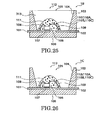
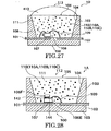
- Figs. 25 through 27 shows devices modified from the devices shown in Figs. 2 through 4 to contain the fluorescent element 110 in the sealing element 111.
- the same or equivalent components as those already explained with reference to Figs. 1A through 24 are commonly labeled, and their detailed explanation is omitted for simplicity.
- the fluorescent element 110 is a mixture of fluorescent elements 110A, 110B and 110C.
- the invention is not limited to this combination, but any other appropriate combination is also acceptable.
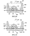
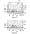
- Figs. 28 through 31 shows devices modified from the devices shown in Figs. 17 and 19 through 21 to contain the fluorescent element 110 in the sealing element 111.
- the same or equivalent components as those already explained with reference to Figs. 1A through 27 are commonly labeled, and their detailed explanation is omitted for simplicity.
- the fluorescent element 110 is a mixture of fluorescent elements 110A, 110B and 110C.
- the invention is not limited to this combination, but any other appropriate combination is also acceptable.
- the embodiment shown here is not limited to devices combining the fluorescent element with the sealing element 111 in the devices according to the first and second. embodiments of the invention. Hereinbelow, some such other specific examples are introduced.
- Fig. 32 is a cross-sectional view that schematically shows a configuration of the substantial part of a light emitting device according to another embodiment of the invention.
- the same or equivalent components as those already explained with reference to Figs. 1A through 31 are commonly labeled, and their detailed explanation is omitted for simplicity.
- the light emitting device shown here also includes a resin stem 100, a stacked structure including a protective diode 106E and a semiconductor light emitting element 106F mounted thereon, and sealing element 111 embedding the stacked structure.
- the sealing element 111 is made of silicone resin having a hardness in a range from 50 through 90 in JISA value.
- the florescent element 110 is included in the silicone resin.
- the resin portion 103 has no side wall around the sealing element 111 such that the secondary light from the fluorescent element 110 both upwardly and laterally to realize a wide luminous intensity profile. This is suitable for applications expected to provide a wide field of view or a wide field of emission.
- Shapes of the sealing element and the resin stem 100 are not limited to those illustrated.
- the sealing element may be hemispherical as shown in Fig. 33, and the resin stem 100 may have a resin portion 103 configured to bury the leads 101, 102 and surround the element with a low side wall.
- Fig. 34 is a cross-sectional view that schematically shows a configuration of the substantial part of a light emitting device according to an embodiment of the invention.
- the same or equivalent components as those already explained with reference to Figs. 1A through 33 are commonly labeled, and their detailed explanation is omitted for simplicity.
- the light emitting device shown here also includes a pair of leads 101, 102.
- the first lead 101 has formed a cup portion 601 at the distal end, and the stacked structure including the protective diode 106E and the light emitting element 106F is mounted at the bottom of the cup portion 601. Then the wire 109 extending from the diode 106E is connected to the lead 102.
- the sealing element 111 containing the fluorescent element 110 is formed to embed these components.
- the sealing element 111 is made of silicone resin having a hardness in a range from 50 through 90 in JISA value.
- the inner side wall surface of the cup portion 601 serves as the reflective surface to reflect the primary light from the light emitting element 106 upwardly. In receipt of the primary light, the fluorescent element 110 releases secondary light of predetermined wavelengths.
- the light emitting device shown here replaces conventional lamp-type semiconductor devices, and is operative as a general-purpose light emitting device having a relatively wide field of emission.
- Fig. 35 is a cross-sectional view that schematically shows a configuration of the substantial part of a light emitting device according to another embodiment of the invention.
- the same or equivalent components as those already explained with reference to Figs. 1A through 34 are commonly labeled, and their detailed explanation is omitted for simplicity.
- the light emitting device shown here has a structure similar to the light emitting device shown in fig. 34.
- the light emitting device also has a cup portion 601 at the distal end of the first lead 101, and the stacked structure including the protective diode 106E and the light emitting element 106F is mounted at the bottom thereof. Then the wire 109 from the diode 106F is connected to the lead 102.
- the sealing element 111 is made of silicone resin having a hardness in a range from 50 through 90 in JISA value.
- the sealing element 111 containing the fluorescent element 110 is provided to embed those components.
- the sealing element 111 is small-sized, and a transparent element 713 is provided to enclose the sealing element 111.
- the small-sized sealing element 111 containing the fluorescent element 110 diminishes the emission portion and increases the luminance.
- the top surface of the transparent element 713 functions as a lens to gather rays of light, and makes it possible to extract converged light as well.
- the transparent element 713 enclosing the sealing element 111 isolates the fluorescent element 110 from the outside atmosphere and improves its durability against moisture and corrosive atmosphere.
- the transparent element may be made of a resin. Especially, an epoxy resin or silicone resin is advantageous for close contact with the sealing element 111 to enhance the resistance to whether and the mechanical strength.
- the sealing element 111 containing the fluorescent element 110 may be limited only on the cup portion 601 to reduce the size of the emission portion and thereby increase the luminance.
- the wire 109 will extend beyond the boundary between the sealing element 111 and the transparent element 713.
- the sealing element 111 and the transparent element 713 are made of similar materials, the stress at the boundary will be minimized and will prevent breakage of wire.
Landscapes
- Engineering & Computer Science (AREA)
- Chemical & Material Sciences (AREA)
- Combustion & Propulsion (AREA)
- Mechanical Engineering (AREA)
- General Engineering & Computer Science (AREA)
- Led Device Packages (AREA)
- Structures Or Materials For Encapsulating Or Coating Semiconductor Devices Or Solid State Devices (AREA)
- Semiconductor Lasers (AREA)
Applications Claiming Priority (2)
| Application Number | Priority Date | Filing Date | Title |
|---|---|---|---|
| JP2001110676 | 2001-04-09 | ||
| JP2001110676A JP2002314143A (ja) | 2001-04-09 | 2001-04-09 | 発光装置 |
Publications (2)
| Publication Number | Publication Date |
|---|---|
| EP1249874A2 true EP1249874A2 (de) | 2002-10-16 |
| EP1249874A3 EP1249874A3 (de) | 2008-06-04 |
Family
ID=18962399
Family Applications (1)
| Application Number | Title | Priority Date | Filing Date |
|---|---|---|---|
| EP20020007367 Withdrawn EP1249874A3 (de) | 2001-04-09 | 2002-04-08 | Lichtemittierende Vorrichtung |
Country Status (5)
| Country | Link |
|---|---|
| US (2) | US6747293B2 (de) |
| EP (1) | EP1249874A3 (de) |
| JP (1) | JP2002314143A (de) |
| KR (3) | KR20020079516A (de) |
| CN (2) | CN1231980C (de) |
Cited By (17)
| Publication number | Priority date | Publication date | Assignee | Title |
|---|---|---|---|---|
| WO2003049204A3 (de) * | 2001-11-30 | 2004-04-29 | Osram Opto Semiconductors Gmbh | Optoelektronisches bauelement |
| EP1267423A3 (de) * | 2001-06-15 | 2004-06-23 | Toyoda Gosei Co., Ltd. | Vergussmasse für einer Leuchtdiode |
| WO2005062393A3 (en) * | 2003-12-09 | 2006-01-05 | Cree Inc | Semiconductor light emitting devices and submounts and methods for forming the same |
| WO2006006544A1 (en) * | 2004-07-09 | 2006-01-19 | Matsushita Electric Industrial Co., Ltd. | Light-emitting device |
| WO2007006378A1 (de) * | 2005-07-08 | 2007-01-18 | Tridonic Optoelectronics Gmbh | Optoelektronische bauelemente mit haftvermittler |
| WO2007126720A3 (en) * | 2006-04-27 | 2008-01-03 | Cree Inc | Submounts for semiconductor light emitting device packages and semiconductor light emitting device packages including the same |
| US7416906B2 (en) | 2005-05-18 | 2008-08-26 | Asahi Rubber Inc. | Soldering method for semiconductor optical device, and semiconductor optical device |
| EP1663706A4 (de) * | 2003-09-08 | 2008-11-05 | Odelo Gmbh | Led-lichtquelle |
| DE102007035684A1 (de) * | 2007-06-05 | 2008-12-11 | Seoul Semiconductor Co., Ltd. | LED-Gehäuse |
| WO2009103285A1 (de) * | 2008-02-22 | 2009-08-27 | Osram Opto Semiconductors Gmbh | Optoelektronisches bauteil |
| EP1794808A4 (de) * | 2004-09-10 | 2009-09-23 | Seoul Semiconductor Co Ltd | Leuchtdiodenkapselung mit mehreren formharzen |
| US8188492B2 (en) | 2006-08-29 | 2012-05-29 | Seoul Semiconductor Co., Ltd. | Light emitting device having plural light emitting diodes and at least one phosphor for emitting different wavelengths of light |
| US9373607B2 (en) | 2011-08-18 | 2016-06-21 | Lg Display Co., Ltd. | Light emitting diode package |
| US9681566B2 (en) | 2010-05-27 | 2017-06-13 | Osram Opto Semiconductors Gmbh | Electronic arrangement and method for producing an electronic arrangement |
| EP1604385B1 (de) * | 2003-03-10 | 2019-12-11 | OSRAM Opto Semiconductors GmbH | Optoelektronisches bauelement mit einem gehäusekörper aus kunststoffmaterial |
| WO2020011798A1 (de) * | 2018-07-13 | 2020-01-16 | Osram Gmbh | Led-anordnung und beleuchtungsvorrichtung |
| WO2024068590A1 (de) * | 2022-09-26 | 2024-04-04 | Ams-Osram International Gmbh | Verfahren zur herstellung eines optoelektronischen bauteils und optoelektronisches bauteil |
Families Citing this family (196)
| Publication number | Priority date | Publication date | Assignee | Title |
|---|---|---|---|---|
| JP2002314138A (ja) * | 2001-04-09 | 2002-10-25 | Toshiba Corp | 発光装置 |
| JP4101468B2 (ja) * | 2001-04-09 | 2008-06-18 | 豊田合成株式会社 | 発光装置の製造方法 |
| USD534505S1 (en) * | 2001-12-28 | 2007-01-02 | Nichia Corporation | Light emitting diode |
| USD565516S1 (en) | 2001-12-28 | 2008-04-01 | Nichia Corporation | Light emitting diode |
| USD557224S1 (en) | 2001-12-28 | 2007-12-11 | Nichia Corporation | Light emitting diode |
| USD547736S1 (en) | 2001-12-28 | 2007-07-31 | Nichia Corporation | Light emitting diode |
| DE10237084A1 (de) * | 2002-08-05 | 2004-02-19 | Osram Opto Semiconductors Gmbh | Verfahren zum Herstellen eines elektrischen Leiterrahmens und Verfahren zum Herstellen eines oberflächenmontierbaren Halbleiterbauelements |
| JP4360788B2 (ja) * | 2002-08-29 | 2009-11-11 | シチズン電子株式会社 | 液晶表示板用のバックライト及びそれに用いる発光ダイオードの製造方法 |
| TWI292961B (en) * | 2002-09-05 | 2008-01-21 | Nichia Corp | Semiconductor device and an optical device using the semiconductor device |
| USD537047S1 (en) | 2002-09-05 | 2007-02-20 | Nichia Corporation | Light emitting diode |
| USD536672S1 (en) | 2002-09-05 | 2007-02-13 | Nichia Corporation | Light emitting diode |
| JP2004186168A (ja) * | 2002-11-29 | 2004-07-02 | Shin Etsu Chem Co Ltd | 発光ダイオード素子用シリコーン樹脂組成物 |
| JP2004266246A (ja) | 2003-02-12 | 2004-09-24 | Toyoda Gosei Co Ltd | 発光装置 |
| TW200427111A (en) | 2003-03-12 | 2004-12-01 | Shinetsu Chemical Co | Material for coating/protecting light-emitting semiconductor and the light-emitting semiconductor device |
| US7633093B2 (en) * | 2003-05-05 | 2009-12-15 | Lighting Science Group Corporation | Method of making optical light engines with elevated LEDs and resulting product |
| US7528421B2 (en) * | 2003-05-05 | 2009-05-05 | Lamina Lighting, Inc. | Surface mountable light emitting diode assemblies packaged for high temperature operation |
| US7777235B2 (en) | 2003-05-05 | 2010-08-17 | Lighting Science Group Corporation | Light emitting diodes with improved light collimation |
| US7157745B2 (en) * | 2004-04-09 | 2007-01-02 | Blonder Greg E | Illumination devices comprising white light emitting diodes and diode arrays and method and apparatus for making them |
| TWI373150B (en) | 2003-07-09 | 2012-09-21 | Shinetsu Chemical Co | Silicone rubber composition, light-emitting semiconductor embedding/protecting material and light-emitting semiconductor device |
| JP4586967B2 (ja) * | 2003-07-09 | 2010-11-24 | 信越化学工業株式会社 | 発光半導体被覆保護材及び発光半導体装置 |
| US7723740B2 (en) * | 2003-09-18 | 2010-05-25 | Nichia Corporation | Light emitting device |
| JP2005093913A (ja) * | 2003-09-19 | 2005-04-07 | Nichia Chem Ind Ltd | 発光装置 |
| TWI291770B (en) | 2003-11-14 | 2007-12-21 | Hon Hai Prec Ind Co Ltd | Surface light source device and light emitting diode |
| JP4803339B2 (ja) | 2003-11-20 | 2011-10-26 | 信越化学工業株式会社 | エポキシ・シリコーン混成樹脂組成物及び発光半導体装置 |
| CN100377370C (zh) * | 2003-11-22 | 2008-03-26 | 鸿富锦精密工业(深圳)有限公司 | 发光二极管和面光源装置 |
| US7087465B2 (en) * | 2003-12-15 | 2006-08-08 | Philips Lumileds Lighting Company, Llc | Method of packaging a semiconductor light emitting device |
| JP2005183531A (ja) * | 2003-12-17 | 2005-07-07 | Sharp Corp | 半導体発光装置 |
| JP4309242B2 (ja) * | 2003-12-19 | 2009-08-05 | Necライティング株式会社 | 赤色蛍光体材料、赤色蛍光体材料を用いた白色発光ダイオードおよび白色発光ダイオードを用いた照明機器 |
| DE10361650A1 (de) * | 2003-12-30 | 2005-08-04 | Osram Opto Semiconductors Gmbh | Optoelektronisches Modul und Verfahren zu dessen Herstellung |
| JP4614679B2 (ja) * | 2004-01-29 | 2011-01-19 | 京セラ株式会社 | 発光装置およびその製造方法ならびに照明装置 |
| JP4163641B2 (ja) * | 2004-02-25 | 2008-10-08 | 株式会社東芝 | Led素子 |
| JP4632677B2 (ja) * | 2004-03-11 | 2011-02-16 | オリンパス株式会社 | 内視鏡装置 |
| JP2006066868A (ja) * | 2004-03-23 | 2006-03-09 | Toyoda Gosei Co Ltd | 固体素子および固体素子デバイス |
| KR100707870B1 (ko) * | 2004-04-27 | 2007-04-13 | 럭스피아(주) | 복수개의 발광 다이오드칩이 배치된 발광 다이오드 패캐지 |
| JP4300418B2 (ja) | 2004-04-30 | 2009-07-22 | 信越化学工業株式会社 | エポキシ・シリコーン混成樹脂組成物及び発光半導体装置 |
| JP4593974B2 (ja) * | 2004-05-27 | 2010-12-08 | 京セラ株式会社 | 発光装置および照明装置 |
| EP1763896B1 (de) * | 2004-06-30 | 2018-10-03 | OSRAM Opto Semiconductors GmbH | Leuchtdiodenanordnung und optisches aufzeichnungsgerät |
| WO2006005062A2 (en) * | 2004-06-30 | 2006-01-12 | Cree, Inc. | Chip-scale methods for packaging light emitting devices and chip-scale packaged light emitting devices |
| JP2006019598A (ja) * | 2004-07-05 | 2006-01-19 | Citizen Electronics Co Ltd | 発光ダイオード |
| KR100674827B1 (ko) * | 2004-07-28 | 2007-01-25 | 삼성전기주식회사 | 백라이트 유니트용 led 패키지 |
| JP4547569B2 (ja) * | 2004-08-31 | 2010-09-22 | スタンレー電気株式会社 | 表面実装型led |
| JP2006093299A (ja) * | 2004-09-22 | 2006-04-06 | Okumura Yu-Ki Co Ltd | 電飾装置 |
| JP2006087572A (ja) * | 2004-09-22 | 2006-04-06 | Okumura Yu-Ki Co Ltd | 電飾装置 |
| JP4166206B2 (ja) * | 2004-09-30 | 2008-10-15 | 共立エレックス株式会社 | 反射板及び発光ダイオード用パッケージ並びに発光ダイオード |
| TWI405349B (zh) * | 2004-10-07 | 2013-08-11 | 首爾半導體股份有限公司 | 側照明透鏡以及使用此透鏡的發光元件 |
| TWM271255U (en) * | 2004-10-08 | 2005-07-21 | Bright Led Electronics Corp | High-power surface-mounted light-emitting diode with high heat dissipation property |
| TWI257714B (en) * | 2004-10-20 | 2006-07-01 | Arima Optoelectronics Corp | Light-emitting device using multilayer composite metal plated layer as flip-chip electrode |
| JP4796293B2 (ja) * | 2004-11-04 | 2011-10-19 | 株式会社 日立ディスプレイズ | 照明装置の製造方法 |
| JP2006186158A (ja) * | 2004-12-28 | 2006-07-13 | Sharp Corp | 発光ダイオードランプおよび発光ダイオード表示装置 |
| JP4634810B2 (ja) * | 2005-01-20 | 2011-02-16 | 信越化学工業株式会社 | シリコーン封止型led |
| JP4143074B2 (ja) * | 2005-02-25 | 2008-09-03 | トキコーポレーション株式会社 | 発光ダイオード |
| JP2006245020A (ja) * | 2005-02-28 | 2006-09-14 | Sharp Corp | 発光ダイオード素子とその製造方法 |
| JP2006253215A (ja) * | 2005-03-08 | 2006-09-21 | Sharp Corp | 発光装置 |
| KR100663906B1 (ko) * | 2005-03-14 | 2007-01-02 | 서울반도체 주식회사 | 발광 장치 |
| KR100593933B1 (ko) * | 2005-03-18 | 2006-06-30 | 삼성전기주식회사 | 산란 영역을 갖는 측면 방출형 발광다이오드 패키지 및이를 포함하는 백라이트 장치 |
| JP2006310771A (ja) * | 2005-03-30 | 2006-11-09 | Toshiba Discrete Technology Kk | 半導体発光装置 |
| JP4744178B2 (ja) * | 2005-04-08 | 2011-08-10 | シャープ株式会社 | 発光ダイオード |
| US20060270808A1 (en) * | 2005-05-24 | 2006-11-30 | Shin-Etsu Chemical Co., Ltd. | Epoxy-silicone mixed resin composition, cured article thereof, and light-emitting semiconductor device |
| KR100650191B1 (ko) * | 2005-05-31 | 2006-11-27 | 삼성전기주식회사 | 정전기 방전 충격에 대한 보호 기능이 내장된 고휘도 발광다이오드 |
| TWI422044B (zh) * | 2005-06-30 | 2014-01-01 | 克立公司 | 封裝發光裝置之晶片尺度方法及經晶片尺度封裝之發光裝置 |
| DE102005034793B3 (de) * | 2005-07-21 | 2007-04-19 | G.L.I. Global Light Industries Gmbh | Lichtemittierende Halbleiterdiode hoher Lichtleistung |
| US7736070B2 (en) * | 2005-08-31 | 2010-06-15 | Avago Technologies Ecbu Ip (Singapore) Pte. Ltd. | Double mold optocoupler |
| JP4945106B2 (ja) * | 2005-09-08 | 2012-06-06 | スタンレー電気株式会社 | 半導体発光装置 |
| US20070063213A1 (en) * | 2005-09-21 | 2007-03-22 | Lighthouse Technology Co., Ltd. | LED package |
| US20070096133A1 (en) * | 2005-11-02 | 2007-05-03 | Lee Kian S | System and method for LED manufacturing |
| JP2007180326A (ja) * | 2005-12-28 | 2007-07-12 | Showa Denko Kk | 発光装置 |
| US8044412B2 (en) | 2006-01-20 | 2011-10-25 | Taiwan Semiconductor Manufacturing Company, Ltd | Package for a light emitting element |
| KR100828891B1 (ko) | 2006-02-23 | 2008-05-09 | 엘지이노텍 주식회사 | Led 패키지 |
| JP5130680B2 (ja) * | 2006-03-02 | 2013-01-30 | 日亜化学工業株式会社 | 半導体装置およびその形成方法 |
| KR100783251B1 (ko) * | 2006-04-10 | 2007-12-06 | 삼성전기주식회사 | 양자점을 이용한 다층 구조 백색 발광 다이오드 및 그의제조방법 |
| JP4952233B2 (ja) * | 2006-04-19 | 2012-06-13 | 日亜化学工業株式会社 | 半導体装置 |
| US7521727B2 (en) * | 2006-04-26 | 2009-04-21 | Rohm And Haas Company | Light emitting device having improved light extraction efficiency and method of making same |
| TWI303494B (en) * | 2006-04-26 | 2008-11-21 | Everlight Electronics Co Ltd | Surface mounting optoelectronic device |
| CN100555629C (zh) * | 2006-05-08 | 2009-10-28 | 亿光电子工业股份有限公司 | 发光二极管封装结构 |
| WO2007135707A1 (ja) | 2006-05-18 | 2007-11-29 | Nichia Corporation | 樹脂成形体及び表面実装型発光装置並びにそれらの製造方法 |
| JP2007324417A (ja) * | 2006-06-01 | 2007-12-13 | Sharp Corp | 半導体発光装置とその製造方法 |
| TWM302123U (en) * | 2006-06-13 | 2006-12-01 | Lighthouse Technology Co Ltd | The stand structure of light-emitting diode |
| US8044418B2 (en) | 2006-07-13 | 2011-10-25 | Cree, Inc. | Leadframe-based packages for solid state light emitting devices |
| US7960819B2 (en) * | 2006-07-13 | 2011-06-14 | Cree, Inc. | Leadframe-based packages for solid state emitting devices |
| KR100780215B1 (ko) | 2006-07-27 | 2007-11-27 | 삼성전기주식회사 | 다수의 엘이디가 실장된 엘이디 패키지 |
| US20080123023A1 (en) * | 2006-08-30 | 2008-05-29 | Trung Doan | White light unit, backlight unit and liquid crystal display device using the same |
| JP4718405B2 (ja) * | 2006-09-19 | 2011-07-06 | シャープ株式会社 | 照明装置 |
| JP4306772B2 (ja) | 2006-10-05 | 2009-08-05 | 日亜化学工業株式会社 | 発光装置 |
| TW200824142A (en) * | 2006-11-22 | 2008-06-01 | Lighthouse Technology Co Ltd | High power diode holder and thereof package is described |
| KR100845856B1 (ko) * | 2006-12-21 | 2008-07-14 | 엘지전자 주식회사 | 발광 소자 패키지 및 그 제조방법 |
| KR20080065451A (ko) * | 2007-01-09 | 2008-07-14 | 삼성전기주식회사 | Led 패키지 |
| US7781783B2 (en) * | 2007-02-07 | 2010-08-24 | SemiLEDs Optoelectronics Co., Ltd. | White light LED device |
| US8093713B2 (en) * | 2007-02-09 | 2012-01-10 | Infineon Technologies Ag | Module with silicon-based layer |
| US8421088B2 (en) | 2007-02-22 | 2013-04-16 | Sharp Kabushiki Kaisha | Surface mounting type light emitting diode |
| US8604506B2 (en) | 2007-02-22 | 2013-12-10 | Sharp Kabushiki Kaisha | Surface mounting type light emitting diode and method for manufacturing the same |
| JP2008251664A (ja) * | 2007-03-29 | 2008-10-16 | Toshiba Lighting & Technology Corp | 照明装置 |
| JP4795293B2 (ja) * | 2007-03-30 | 2011-10-19 | ローム株式会社 | 半導体発光装置 |
| KR20100028033A (ko) * | 2007-05-09 | 2010-03-11 | 씨. 아이. 카세이 가부시기가이샤 | 발광장치 및 발광장치용 패키지 집합체 |
| JP2008300573A (ja) * | 2007-05-30 | 2008-12-11 | Toshiba Corp | 発光装置 |
| JP5233170B2 (ja) * | 2007-05-31 | 2013-07-10 | 日亜化学工業株式会社 | 発光装置、発光装置を構成する樹脂成形体及びそれらの製造方法 |
| JPWO2009008210A1 (ja) * | 2007-07-11 | 2010-09-02 | シーアイ化成株式会社 | 発光装置 |
| USD576573S1 (en) * | 2007-07-17 | 2008-09-09 | Rohm Co., Ltd. | Light emitting diode module |
| JP2009094199A (ja) * | 2007-10-05 | 2009-04-30 | Sharp Corp | 発光装置、面光源、表示装置と、その製造方法 |
| JP5514112B2 (ja) * | 2007-10-09 | 2014-06-04 | フィリップス ソリッド−ステート ライティング ソリューションズ インコーポレイテッド | 複数の直列接続された負荷のそれぞれの負荷電流を制御するための方法及び装置 |
| KR20090069842A (ko) * | 2007-12-26 | 2009-07-01 | 삼성에스디아이 주식회사 | 백색 형광체, 이를 이용하는 발광 유닛, 및 이 발광 유닛을갖는 표시 장치 |
| CN101538367B (zh) | 2008-01-28 | 2013-09-04 | 信越化学工业株式会社 | 二缩水甘油基异氰尿酸基改性有机聚硅氧烷以及含有该有机聚硅氧烷的组成物 |
| CN101533819B (zh) * | 2008-03-14 | 2013-01-16 | 旭丽电子(广州)有限公司 | 半导体封装构造、应用于半导体封装构造的导线架及导电件 |
| KR20100003320A (ko) * | 2008-06-24 | 2010-01-08 | 엘지이노텍 주식회사 | 발광 다이오드 패키지 |
| EP2313936A4 (de) * | 2008-07-16 | 2017-06-28 | 3M Innovative Properties Company | Stabile lichtquelle |
| JP5464825B2 (ja) | 2008-07-23 | 2014-04-09 | ローム株式会社 | Ledモジュール |
| JP2010032732A (ja) * | 2008-07-28 | 2010-02-12 | Panasonic Corp | 液晶表示装置 |
| JP2010031149A (ja) | 2008-07-29 | 2010-02-12 | Shin-Etsu Chemical Co Ltd | 光半導体素子封止用樹脂組成物 |
| JP5217800B2 (ja) * | 2008-09-03 | 2013-06-19 | 日亜化学工業株式会社 | 発光装置、樹脂パッケージ、樹脂成形体並びにこれらの製造方法 |
| US20100116970A1 (en) * | 2008-11-12 | 2010-05-13 | Wen-Long Chou | Photo detection device |
| JP4403199B2 (ja) * | 2008-11-17 | 2010-01-20 | 株式会社東芝 | 発光装置 |
| TWI384591B (zh) * | 2008-11-17 | 2013-02-01 | 億光電子工業股份有限公司 | 發光二極體電路板 |
| US8288785B2 (en) * | 2008-12-03 | 2012-10-16 | Seoul Semiconductor Co., Ltd. | Lead frame having light-reflecting layer, light emitting diode having the lead frame, and backlight unit having the light emitting diode |
| JP5368809B2 (ja) * | 2009-01-19 | 2013-12-18 | ローム株式会社 | Ledモジュールの製造方法およびledモジュール |
| JP5340763B2 (ja) * | 2009-02-25 | 2013-11-13 | ローム株式会社 | Ledランプ |
| US8610156B2 (en) | 2009-03-10 | 2013-12-17 | Lg Innotek Co., Ltd. | Light emitting device package |
| TWI378578B (en) * | 2009-03-25 | 2012-12-01 | Coretronic Corp | Light emitting diode package |
| JP5327042B2 (ja) * | 2009-03-26 | 2013-10-30 | 豊田合成株式会社 | Ledランプの製造方法 |
| CN101859757B (zh) * | 2009-04-07 | 2014-04-09 | 裕星企业有限公司 | 堆栈发光二极管芯片结构及其制造方法 |
| KR101060761B1 (ko) * | 2009-04-23 | 2011-08-31 | 삼성엘이디 주식회사 | 발광 다이오드 패키지 |
| JP5251919B2 (ja) | 2009-05-08 | 2013-07-31 | 信越化学工業株式会社 | 光半導体素子封止用樹脂組成物 |
| JP5305452B2 (ja) | 2009-06-12 | 2013-10-02 | 信越化学工業株式会社 | 光半導体素子封止用樹脂組成物 |
| KR101064090B1 (ko) * | 2009-11-17 | 2011-09-08 | 엘지이노텍 주식회사 | 발광소자 패키지 |
| JP4951090B2 (ja) * | 2010-01-29 | 2012-06-13 | 株式会社東芝 | Ledパッケージ |
| KR101047778B1 (ko) * | 2010-04-01 | 2011-07-07 | 엘지이노텍 주식회사 | 발광 소자 패키지 및 이를 구비한 라이트 유닛 |
| JP5489280B2 (ja) | 2010-04-07 | 2014-05-14 | 信越化学工業株式会社 | 光半導体封止用エポキシ組成物 |
| DE112011101327T5 (de) | 2010-04-15 | 2013-01-31 | Citizen Electronics Co., Ltd. | Licht aussendende Vorrichtung |
| CN105931696B (zh) | 2010-04-23 | 2017-07-07 | 皮瑟莱根特科技有限责任公司 | 纳米晶体的合成、盖帽和分散 |
| TWI561770B (en) * | 2010-04-30 | 2016-12-11 | Samsung Electronics Co Ltd | Light emitting device package, light source module, backlight unit, display apparatus, television set, and illumination apparatus |
| JP5528900B2 (ja) * | 2010-04-30 | 2014-06-25 | ローム株式会社 | 発光素子モジュール |
| KR101115536B1 (ko) * | 2010-05-11 | 2012-02-27 | 서울옵토디바이스주식회사 | 다색 발광 다이오드 |
| KR101039994B1 (ko) * | 2010-05-24 | 2011-06-09 | 엘지이노텍 주식회사 | 발광소자 및 이를 구비한 라이트 유닛 |
| JP2012019062A (ja) | 2010-07-08 | 2012-01-26 | Shin Etsu Chem Co Ltd | 発光半導体装置、実装基板及びそれらの製造方法 |
| DE102011003608A1 (de) * | 2010-08-20 | 2012-02-23 | Tridonic Gmbh & Co. Kg | Gehäustes LED-Modul |
| KR20120024104A (ko) * | 2010-09-06 | 2012-03-14 | 서울옵토디바이스주식회사 | 발광 소자 |
| JP2012069589A (ja) * | 2010-09-21 | 2012-04-05 | Toshiba Corp | 発光装置 |
| USD658606S1 (en) * | 2010-09-29 | 2012-05-01 | Kabushiki Kaisha Toshiba | Portion of a light-emitting diode |
| JP2014503446A (ja) | 2010-10-27 | 2014-02-13 | ピクセリジェント・テクノロジーズ,エルエルシー | ナノ結晶の合成、キャップ形成および分散 |
| US20120138981A1 (en) * | 2010-12-02 | 2012-06-07 | Chung-Shan Institute of Science and Technology, Armaments, Bureau, Ministry of National Defense | Light-Emitting Diode Apparatus and Method for Making the Same |
| KR101626412B1 (ko) | 2010-12-24 | 2016-06-02 | 삼성전자주식회사 | 발광소자 패키지 및 그 제조방법 |
| CN102157505A (zh) * | 2011-01-20 | 2011-08-17 | 日月光半导体制造股份有限公司 | 发光模块 |
| JP4870233B1 (ja) * | 2011-02-14 | 2012-02-08 | E&E Japan株式会社 | チップled |
| JP5753446B2 (ja) * | 2011-06-17 | 2015-07-22 | 株式会社東芝 | 半導体発光装置の製造方法 |
| JP5852339B2 (ja) * | 2011-06-21 | 2016-02-03 | ローム株式会社 | 光源装置および画像読取装置 |
| US8704433B2 (en) | 2011-08-22 | 2014-04-22 | Lg Innotek Co., Ltd. | Light emitting device package and light unit |
| US9359689B2 (en) | 2011-10-26 | 2016-06-07 | Pixelligent Technologies, Llc | Synthesis, capping and dispersion of nanocrystals |
| USD674757S1 (en) * | 2011-10-31 | 2013-01-22 | Silitek Electronics (Guangzhou) Co., Ltd. | Package carrier of light emitting diode |
| USD674758S1 (en) * | 2011-10-31 | 2013-01-22 | Silitek Electronic (Guangzhou) Co., Ltd. | Light emitting diode |
| JP5865038B2 (ja) * | 2011-11-30 | 2016-02-17 | 日東電工株式会社 | 素子接続用基板、その製造方法および発光ダイオード装置 |
| DE102011056706B4 (de) * | 2011-12-20 | 2016-12-15 | Osram Opto Semiconductors Gmbh | Verfahren zur Herstellung von optoelektronischen Halbleiterbauteilen, Anordnung und optoelektronisches Halbleiterbauteil |
| US20130161670A1 (en) * | 2011-12-23 | 2013-06-27 | Sheng-Yang Peng | Light emitting diode packages and methods of making |
| CN102593321B (zh) * | 2012-02-20 | 2015-11-25 | 深圳市安普光光电科技有限公司 | Led的封装方法、led封装结构及显示屏 |
| US20130249387A1 (en) * | 2012-03-20 | 2013-09-26 | Chia-Fen Hsin | Light-emitting diodes, packages, and methods of making |
| JP5935078B2 (ja) * | 2012-05-22 | 2016-06-15 | パナソニックIpマネジメント株式会社 | Ledモジュールおよびその製造方法、照明器具、直管形ledランプ |
| JP5927056B2 (ja) * | 2012-06-14 | 2016-05-25 | ルネサスエレクトロニクス株式会社 | 半導体装置 |
| CN104412379B (zh) * | 2012-06-28 | 2017-02-22 | 株式会社村田制作所 | 电子部件的罐封装件结构 |
| US9755126B2 (en) | 2012-07-30 | 2017-09-05 | Ushio Denki Kabushiki Kaisha | Light source unit |
| TWM450831U (zh) * | 2012-11-23 | 2013-04-11 | 海立爾股份有限公司 | 具有散熱單元之高亮度發光二極體燈具結構 |
| KR102114931B1 (ko) * | 2012-12-18 | 2020-05-25 | 엘지이노텍 주식회사 | 발광소자 패키지 |
| EP2948709B1 (de) | 2013-01-25 | 2016-10-05 | Koninklijke Philips N.V. | Beleuchtungsaufbau und verfahen für herrstelling eines beleuchtungsaufbaus |
| US20140208689A1 (en) | 2013-01-25 | 2014-07-31 | Renee Joyal | Hypodermic syringe assist apparatus and method |
| DE102013103416A1 (de) * | 2013-04-05 | 2014-10-23 | Osram Opto Semiconductors Gmbh | Elektromagnetische Strahlung emittierende Baugruppe und Verfahren zum Herstellen einer elektromagnetische Strahlung emittierenden Baugruppe |
| KR102175729B1 (ko) * | 2013-08-09 | 2020-11-06 | 스미또모 가가꾸 가부시키가이샤 | 광학 필름 |
| KR102270798B1 (ko) * | 2013-12-16 | 2021-06-30 | 삼성메디슨 주식회사 | 광음향 프로브 및 광음향 진단 장치 |
| WO2015092579A1 (en) * | 2013-12-18 | 2015-06-25 | Koninklijke Philips N.V. | Reflective solder mask layer for led phosphor package |
| KR102122361B1 (ko) | 2013-12-27 | 2020-06-15 | 삼성전자주식회사 | 플립칩 엘이디 패키지 기판 및 플립칩 엘이디 패키지 구조 |
| DE102014110473A1 (de) | 2014-07-24 | 2016-01-28 | Osram Opto Semiconductors Gmbh | Träger für ein elektrisches Bauelement |
| US10205069B2 (en) | 2014-07-31 | 2019-02-12 | Bridgelux Inc. | LED array package |
| KR102273653B1 (ko) * | 2014-08-29 | 2021-07-06 | 서울반도체 주식회사 | 발광 다이오드 패키지 |
| KR102256594B1 (ko) * | 2014-10-07 | 2021-05-26 | 서울반도체 주식회사 | 발광 다이오드 패키지 |
| KR102256593B1 (ko) * | 2014-10-08 | 2021-05-26 | 서울반도체 주식회사 | 발광 다이오드 패키지 |
| EP3546544B1 (de) | 2014-10-08 | 2024-05-01 | Seoul Semiconductor Co., Ltd. | Lichtemittierende vorrichtung |
| KR102288377B1 (ko) * | 2014-11-20 | 2021-08-11 | 서울반도체 주식회사 | 발광 장치 |
| KR102288404B1 (ko) * | 2014-11-20 | 2021-08-11 | 서울반도체 주식회사 | 발광 장치 |
| JP6325471B2 (ja) | 2015-03-02 | 2018-05-16 | 株式会社東芝 | 光結合装置および絶縁装置 |
| DE102015103840A1 (de) * | 2015-03-16 | 2016-09-22 | Osram Opto Semiconductors Gmbh | Elektromagnetische Strahlung emittierende Baugruppe |
| JP2017034218A (ja) * | 2015-08-03 | 2017-02-09 | 株式会社東芝 | 半導体発光装置 |
| JP6626294B2 (ja) | 2015-09-04 | 2019-12-25 | 株式会社東芝 | 半導体装置および光結合装置 |
| JP2017112211A (ja) * | 2015-12-16 | 2017-06-22 | 豊田合成株式会社 | 発光装置の製造方法 |
| CN108366989B (zh) | 2015-12-25 | 2020-11-03 | 富士胶片富山化学株式会社 | 含有1-(3-(2-(1-苯并噻吩-5-基-)乙氧基)丙基)氮杂环丁-3-醇或其盐的片剂 |
| US11677059B2 (en) | 2017-04-26 | 2023-06-13 | Samsung Electronics Co., Ltd. | Light-emitting device package including a lead frame |
| KR102335216B1 (ko) | 2017-04-26 | 2021-12-03 | 삼성전자 주식회사 | 발광소자 패키지 |
| JP7004397B2 (ja) * | 2017-06-09 | 2022-01-21 | ローム株式会社 | 光学装置 |
| CN107479259B (zh) * | 2017-08-25 | 2020-03-24 | 上海天马有机发光显示技术有限公司 | 显示面板和显示装置 |
| JP7037046B2 (ja) | 2018-01-31 | 2022-03-16 | 日亜化学工業株式会社 | 発光装置及びその製造方法 |
| JP6822442B2 (ja) * | 2018-03-01 | 2021-01-27 | 日亜化学工業株式会社 | 発光装置およびその製造方法 |
| JP6645540B2 (ja) * | 2018-08-09 | 2020-02-14 | 日亜化学工業株式会社 | 発光装置用パッケージ成形体及びそれを用いた発光装置 |
| KR102023085B1 (ko) * | 2018-08-16 | 2019-09-19 | 엘지이노텍 주식회사 | 발광소자 패키지 |
| JP7176684B2 (ja) * | 2018-09-19 | 2022-11-22 | 豊田合成株式会社 | 発光装置 |
| JP7248887B2 (ja) * | 2019-02-15 | 2023-03-30 | 日亜化学工業株式会社 | 樹脂パッケージ及び発光装置 |
| JP6842485B2 (ja) * | 2019-03-04 | 2021-03-17 | ローム株式会社 | Ledモジュール |
| TWI819073B (zh) * | 2019-08-22 | 2023-10-21 | 晶元光電股份有限公司 | 發光裝置、其製造方法及顯示模組 |
| DE102020200848A1 (de) | 2020-01-24 | 2021-07-29 | Robert Bosch Gesellschaft mit beschränkter Haftung | Sensorgehäuse und Verfahren zum Vergießen eines offenen Aufnahmeraums eines Sensorgehäuses |
| JP6888709B2 (ja) * | 2020-04-09 | 2021-06-16 | 日亜化学工業株式会社 | 発光装置の製造方法及び発光装置 |
| JP7389363B2 (ja) * | 2021-05-26 | 2023-11-30 | 日亜化学工業株式会社 | 発光装置 |
| JP7797267B2 (ja) * | 2022-03-19 | 2026-01-13 | Hoya株式会社 | 光照射モジュール、光照射装置 |
| CN114927513A (zh) * | 2022-07-21 | 2022-08-19 | 杭州华普永明光电股份有限公司 | 一种发光模组及植物照明灯具 |
Citations (1)
| Publication number | Priority date | Publication date | Assignee | Title |
|---|---|---|---|---|
| US5851847A (en) * | 1995-09-29 | 1998-12-22 | Sony Corporation | Photonic device and process for fabricating the same |
Family Cites Families (47)
| Publication number | Priority date | Publication date | Assignee | Title |
|---|---|---|---|---|
| US36446A (en) * | 1862-09-16 | Improvement in plow-beams | ||
| FR2248663B1 (de) * | 1972-12-13 | 1978-08-11 | Radiotechnique Compelec | |
| US4034466A (en) * | 1974-09-03 | 1977-07-12 | Motorola, Inc. | Package and method for a semiconductor radiant energy emitting device |
| GB1557685A (en) * | 1976-02-02 | 1979-12-12 | Fairchild Camera Instr Co | Optically coupled isolator device |
| DE3019239A1 (de) * | 1980-05-20 | 1981-11-26 | SIEMENS AG AAAAA, 1000 Berlin und 8000 München | Umhuellung fuer halbleiterbauelement |
| JPS60262474A (ja) * | 1984-06-08 | 1985-12-25 | Toshiba Corp | 光半導体装置 |
| JPS6254974A (ja) | 1985-09-04 | 1987-03-10 | Mitsubishi Electric Corp | 光結合半導体装置 |
| US4843280A (en) * | 1988-01-15 | 1989-06-27 | Siemens Corporate Research & Support, Inc. | A modular surface mount component for an electrical device or led's |
| US4890383A (en) | 1988-01-15 | 1990-01-02 | Simens Corporate Research & Support, Inc. | Method for producing displays and modular components |
| JPH0292927U (de) * | 1989-01-11 | 1990-07-24 | ||
| JPH0448674A (ja) * | 1990-06-14 | 1992-02-18 | Rohm Co Ltd | 半導体レーザ |
| JPH0521458A (ja) | 1991-07-11 | 1993-01-29 | Nec Corp | 半導体装置およびその製造方法 |
| JP2715792B2 (ja) * | 1992-02-13 | 1998-02-18 | 信越化学工業株式会社 | 光透過性エポキシ樹脂組成物及び光半導体装置 |
| JPH065742A (ja) * | 1992-06-22 | 1994-01-14 | Mitsubishi Electric Corp | 半導体装置、その封止に用いられる樹脂および半導体装置の製造方法 |
| JP2809951B2 (ja) * | 1992-12-17 | 1998-10-15 | 株式会社東芝 | 半導体発光装置とその製造方法 |
| JP3420612B2 (ja) * | 1993-06-25 | 2003-06-30 | 株式会社東芝 | Ledランプ |
| JPH0745641A (ja) * | 1993-07-30 | 1995-02-14 | Matsushita Electric Works Ltd | 半導体装置の実装方法 |
| JP3648756B2 (ja) * | 1994-03-22 | 2005-05-18 | Jsr株式会社 | 半導体素子用コーテイング材 |
| JPH07278438A (ja) * | 1994-04-14 | 1995-10-24 | Toray Dow Corning Silicone Co Ltd | 電子部品含浸用硬化性オルガノポリシロキサン組成物および電子部品 |
| US5489800A (en) * | 1994-08-31 | 1996-02-06 | Motorola, Inc. | Dual channel small outline optocoupler package and method thereof |
| US5832600A (en) * | 1995-06-06 | 1998-11-10 | Seiko Epson Corporation | Method of mounting electronic parts |
| JPH08335720A (ja) * | 1995-06-08 | 1996-12-17 | Nichia Chem Ind Ltd | 窒化物半導体発光ダイオード |
| US5748161A (en) * | 1996-03-04 | 1998-05-05 | Motorola, Inc. | Integrated electro-optical package with independent menu bar |
| JP3034363U (ja) * | 1996-05-01 | 1997-02-18 | 武雄 稲垣 | 発光素子を内蔵した表示灯 |
| DE19621124A1 (de) * | 1996-05-24 | 1997-11-27 | Siemens Ag | Optoelektronischer Wandler und dessen Herstellungsverfahren |
| DE19638667C2 (de) * | 1996-09-20 | 2001-05-17 | Osram Opto Semiconductors Gmbh | Mischfarbiges Licht abstrahlendes Halbleiterbauelement mit Lumineszenzkonversionselement |
| TW383508B (en) * | 1996-07-29 | 2000-03-01 | Nichia Kagaku Kogyo Kk | Light emitting device and display |
| JP4316019B2 (ja) * | 1996-10-01 | 2009-08-19 | 株式会社東芝 | 半導体装置及び半導体装置製造方法 |
| US6054716A (en) * | 1997-01-10 | 2000-04-25 | Rohm Co., Ltd. | Semiconductor light emitting device having a protecting device |
| JP3673621B2 (ja) * | 1997-07-30 | 2005-07-20 | ローム株式会社 | チップ型発光素子 |
| US6274890B1 (en) * | 1997-01-15 | 2001-08-14 | Kabushiki Kaisha Toshiba | Semiconductor light emitting device and its manufacturing method |
| JP3492178B2 (ja) * | 1997-01-15 | 2004-02-03 | 株式会社東芝 | 半導体発光装置及びその製造方法 |
| US6333522B1 (en) * | 1997-01-31 | 2001-12-25 | Matsushita Electric Industrial Co., Ltd. | Light-emitting element, semiconductor light-emitting device, and manufacturing methods therefor |
| JPH10247748A (ja) * | 1997-03-03 | 1998-09-14 | Omron Corp | 発光素子及び当該発光素子を用いた面光源装置 |
| KR100298880B1 (ko) * | 1997-05-01 | 2001-10-26 | 송기선 | 광결합소자및그제조방법 |
| JP3378465B2 (ja) | 1997-05-16 | 2003-02-17 | 株式会社東芝 | 発光装置 |
| US6037400A (en) * | 1997-08-25 | 2000-03-14 | Hitachi Maxell, Ltd | Composition for prevention of electric wave in wide range and electric wave absorber coping with all directions using same |
| US6340824B1 (en) * | 1997-09-01 | 2002-01-22 | Kabushiki Kaisha Toshiba | Semiconductor light emitting device including a fluorescent material |
| US6147367A (en) * | 1997-12-10 | 2000-11-14 | Industrial Technology Research Institute | Packaging design for light emitting diode |
| JP3618551B2 (ja) * | 1998-06-30 | 2005-02-09 | 株式会社東芝 | 光半導体モジュール |
| US6335548B1 (en) * | 1999-03-15 | 2002-01-01 | Gentex Corporation | Semiconductor radiation emitter package |
| JP4680334B2 (ja) * | 1999-01-13 | 2011-05-11 | 株式会社朝日ラバー | 発光装置 |
| JP2000349348A (ja) * | 1999-03-31 | 2000-12-15 | Toyoda Gosei Co Ltd | 短波長ledランプユニット |
| JP3690968B2 (ja) | 1999-06-30 | 2005-08-31 | 日亜化学工業株式会社 | 発光装置及びその形成方法 |
| EP1113506A3 (de) * | 1999-12-28 | 2005-03-16 | Toyoda Gosei Co., Ltd. | Lichtemittierende Diode |
| CN1173417C (zh) * | 2000-03-17 | 2004-10-27 | 松下电器产业株式会社 | 半导体发光器件及面发光装置 |
| US6867542B1 (en) * | 2000-03-29 | 2005-03-15 | General Electric Company | Floating chip photonic device and method of manufacture |
-
2001
- 2001-04-09 JP JP2001110676A patent/JP2002314143A/ja active Pending
-
2002
- 2002-04-03 CN CNB021186979A patent/CN1231980C/zh not_active Expired - Lifetime
- 2002-04-03 CN CNA200510127175XA patent/CN1797766A/zh active Pending
- 2002-04-08 KR KR1020020019014A patent/KR20020079516A/ko not_active Abandoned
- 2002-04-08 EP EP20020007367 patent/EP1249874A3/de not_active Withdrawn
- 2002-04-08 US US10/118,604 patent/US6747293B2/en not_active Expired - Lifetime
-
2004
- 2004-03-08 US US10/795,839 patent/US20040217369A1/en not_active Abandoned
- 2004-09-24 KR KR10-2004-0077336A patent/KR100514609B1/ko not_active Expired - Fee Related
-
2005
- 2005-02-18 KR KR1020050013570A patent/KR20050039764A/ko not_active Ceased
Patent Citations (1)
| Publication number | Priority date | Publication date | Assignee | Title |
|---|---|---|---|---|
| US5851847A (en) * | 1995-09-29 | 1998-12-22 | Sony Corporation | Photonic device and process for fabricating the same |
Cited By (31)
| Publication number | Priority date | Publication date | Assignee | Title |
|---|---|---|---|---|
| EP1267423A3 (de) * | 2001-06-15 | 2004-06-23 | Toyoda Gosei Co., Ltd. | Vergussmasse für einer Leuchtdiode |
| WO2003049204A3 (de) * | 2001-11-30 | 2004-04-29 | Osram Opto Semiconductors Gmbh | Optoelektronisches bauelement |
| US7514723B2 (en) | 2001-11-30 | 2009-04-07 | Osram Opto Semiconductors Gmbh | Optoelectronic component |
| EP1604385B1 (de) * | 2003-03-10 | 2019-12-11 | OSRAM Opto Semiconductors GmbH | Optoelektronisches bauelement mit einem gehäusekörper aus kunststoffmaterial |
| EP1663706A4 (de) * | 2003-09-08 | 2008-11-05 | Odelo Gmbh | Led-lichtquelle |
| US7518158B2 (en) | 2003-12-09 | 2009-04-14 | Cree, Inc. | Semiconductor light emitting devices and submounts |
| WO2005062393A3 (en) * | 2003-12-09 | 2006-01-05 | Cree Inc | Semiconductor light emitting devices and submounts and methods for forming the same |
| US8138000B2 (en) | 2003-12-09 | 2012-03-20 | Cree, Inc. | Methods for forming semiconductor light emitting devices and submounts |
| US8847257B2 (en) | 2003-12-09 | 2014-09-30 | Cree, Inc. | Semiconductor light emitting devices and submounts |
| WO2006006544A1 (en) * | 2004-07-09 | 2006-01-19 | Matsushita Electric Industrial Co., Ltd. | Light-emitting device |
| EP1794808A4 (de) * | 2004-09-10 | 2009-09-23 | Seoul Semiconductor Co Ltd | Leuchtdiodenkapselung mit mehreren formharzen |
| US7737463B2 (en) | 2004-09-10 | 2010-06-15 | Seoul Semiconductor Co., Ltd. | Light emitting diode package with a heat sink support ring and having multiple molding resins, wherein secondary molding resin with higher hardness than primary molding resin and which covers primary molding resin that covers LED die |
| US7855395B2 (en) | 2004-09-10 | 2010-12-21 | Seoul Semiconductor Co., Ltd. | Light emitting diode package having multiple molding resins on a light emitting diode die |
| US7416906B2 (en) | 2005-05-18 | 2008-08-26 | Asahi Rubber Inc. | Soldering method for semiconductor optical device, and semiconductor optical device |
| US7638812B2 (en) | 2005-05-18 | 2009-12-29 | Asahi Rubber Inc. | Soldering method for semiconductor optical device, and semiconductor optical device |
| US8530914B2 (en) | 2005-07-08 | 2013-09-10 | Tridonicatco Optoelectronics Gmbh | Optoelectronic components with adhesion agent |
| WO2007006378A1 (de) * | 2005-07-08 | 2007-01-18 | Tridonic Optoelectronics Gmbh | Optoelektronische bauelemente mit haftvermittler |
| KR101015194B1 (ko) * | 2005-07-08 | 2011-02-18 | 루미테크 프로둑션 운트 엔트빅룽 게엠베하 | 접착제를 포함하는 광전자 구성요소 |
| US7655957B2 (en) | 2006-04-27 | 2010-02-02 | Cree, Inc. | Submounts for semiconductor light emitting device packages and semiconductor light emitting device packages including the same |
| EP2372801A3 (de) * | 2006-04-27 | 2012-04-11 | Cree, Inc. | Montagebasis für Gehäuse für lichtemittierende Halbleiterbauelemente und Gehäuse für lichtemittierende Halbleiterbauelemente damit |
| US8378374B2 (en) | 2006-04-27 | 2013-02-19 | Cree, Inc. | Semiconductor light emitting device packages including submounts |
| WO2007126720A3 (en) * | 2006-04-27 | 2008-01-03 | Cree Inc | Submounts for semiconductor light emitting device packages and semiconductor light emitting device packages including the same |
| US8188492B2 (en) | 2006-08-29 | 2012-05-29 | Seoul Semiconductor Co., Ltd. | Light emitting device having plural light emitting diodes and at least one phosphor for emitting different wavelengths of light |
| DE102007035684A1 (de) * | 2007-06-05 | 2008-12-11 | Seoul Semiconductor Co., Ltd. | LED-Gehäuse |
| WO2009103285A1 (de) * | 2008-02-22 | 2009-08-27 | Osram Opto Semiconductors Gmbh | Optoelektronisches bauteil |
| US9681566B2 (en) | 2010-05-27 | 2017-06-13 | Osram Opto Semiconductors Gmbh | Electronic arrangement and method for producing an electronic arrangement |
| US10026710B2 (en) | 2010-05-27 | 2018-07-17 | Osram Opto Semiconductors Gmbh | Electronic arrangement |
| US9373607B2 (en) | 2011-08-18 | 2016-06-21 | Lg Display Co., Ltd. | Light emitting diode package |
| WO2020011798A1 (de) * | 2018-07-13 | 2020-01-16 | Osram Gmbh | Led-anordnung und beleuchtungsvorrichtung |
| US11274812B2 (en) | 2018-07-13 | 2022-03-15 | Osram Gmbh | LED arrangement and lighting device |
| WO2024068590A1 (de) * | 2022-09-26 | 2024-04-04 | Ams-Osram International Gmbh | Verfahren zur herstellung eines optoelektronischen bauteils und optoelektronisches bauteil |
Also Published As
| Publication number | Publication date |
|---|---|
| US6747293B2 (en) | 2004-06-08 |
| KR20050039764A (ko) | 2005-04-29 |
| KR100514609B1 (ko) | 2005-09-14 |
| CN1381906A (zh) | 2002-11-27 |
| CN1797766A (zh) | 2006-07-05 |
| KR20020079516A (ko) | 2002-10-19 |
| EP1249874A3 (de) | 2008-06-04 |
| JP2002314143A (ja) | 2002-10-25 |
| US20020190262A1 (en) | 2002-12-19 |
| CN1231980C (zh) | 2005-12-14 |
| KR20040091605A (ko) | 2004-10-28 |
| US20040217369A1 (en) | 2004-11-04 |
Similar Documents
| Publication | Publication Date | Title |
|---|---|---|
| US6747293B2 (en) | Light emitting device | |
| JP3655267B2 (ja) | 半導体発光装置 | |
| US7569989B2 (en) | Light emitting device | |
| EP1249875B1 (de) | Lichtemittierende Vorrichtung | |
| US9929318B2 (en) | Resin molding, surface mounted light emitting apparatus and methods for manufacturing the same | |
| US8525208B2 (en) | Light emitting device | |
| JP4599857B2 (ja) | 半導体装置及びその製造方法 | |
| US7276739B2 (en) | Low thermal resistance light emitting diode | |
| JPWO2008105527A1 (ja) | Led装置及び照明装置 | |
| US10553763B2 (en) | Light emitting device | |
| JP2007329502A (ja) | 発光装置 | |
| JP4403199B2 (ja) | 発光装置 | |
| JP2007329219A (ja) | 樹脂成形体及び表面実装型発光装置並びにそれらの製造方法 | |
| JP4874510B2 (ja) | 発光装置及びその製造方法 | |
| JP4600404B2 (ja) | 半導体装置及びその製造方法 | |
| JP2006093738A (ja) | 半導体装置及びその製造方法 | |
| JP5294741B2 (ja) | 樹脂成形体及び表面実装型発光装置並びにそれらの製造方法 | |
| JP4923711B2 (ja) | 発光装置 |
Legal Events
| Date | Code | Title | Description |
|---|---|---|---|
| PUAI | Public reference made under article 153(3) epc to a published international application that has entered the european phase |
Free format text: ORIGINAL CODE: 0009012 |
|
| 17P | Request for examination filed |
Effective date: 20020408 |
|
| AK | Designated contracting states |
Kind code of ref document: A2 Designated state(s): AT BE CH CY DE DK ES FI FR GB GR IE IT LI LU MC NL PT SE TR |
|
| AX | Request for extension of the european patent |
Free format text: AL;LT;LV;MK;RO;SI |
|
| PUAL | Search report despatched |
Free format text: ORIGINAL CODE: 0009013 |
|
| AK | Designated contracting states |
Kind code of ref document: A3 Designated state(s): AT BE CH CY DE DK ES FI FR GB GR IE IT LI LU MC NL PT SE TR |
|
| AX | Request for extension of the european patent |
Extension state: AL LT LV MK RO SI |
|
| 17Q | First examination report despatched |
Effective date: 20080903 |
|
| AKX | Designation fees paid |
Designated state(s): DE FR GB |
|
| STAA | Information on the status of an ep patent application or granted ep patent |
Free format text: STATUS: THE APPLICATION IS DEEMED TO BE WITHDRAWN |
|
| 18D | Application deemed to be withdrawn |
Effective date: 20150730 |