EP1249876A2 - Lichtemittierende Vorrichtung - Google Patents
Lichtemittierende Vorrichtung Download PDFInfo
- Publication number
- EP1249876A2 EP1249876A2 EP20020007381 EP02007381A EP1249876A2 EP 1249876 A2 EP1249876 A2 EP 1249876A2 EP 20020007381 EP20020007381 EP 20020007381 EP 02007381 A EP02007381 A EP 02007381A EP 1249876 A2 EP1249876 A2 EP 1249876A2
- Authority
- EP
- European Patent Office
- Prior art keywords
- light emitting
- semiconductor
- lead
- emitting element
- emitting device
- Prior art date
- Legal status (The legal status is an assumption and is not a legal conclusion. Google has not performed a legal analysis and makes no representation as to the accuracy of the status listed.)
- Withdrawn
Links
Images


Classifications
-
- H—ELECTRICITY
- H10—SEMICONDUCTOR DEVICES; ELECTRIC SOLID-STATE DEVICES NOT OTHERWISE PROVIDED FOR
- H10W—GENERIC PACKAGES, INTERCONNECTIONS, CONNECTORS OR OTHER CONSTRUCTIONAL DETAILS OF DEVICES COVERED BY CLASS H10
- H10W90/00—Package configurations
-
- H—ELECTRICITY
- H10—SEMICONDUCTOR DEVICES; ELECTRIC SOLID-STATE DEVICES NOT OTHERWISE PROVIDED FOR
- H10H—INORGANIC LIGHT-EMITTING SEMICONDUCTOR DEVICES HAVING POTENTIAL BARRIERS
- H10H20/00—Individual inorganic light-emitting semiconductor devices having potential barriers, e.g. light-emitting diodes [LED]
- H10H20/80—Constructional details
- H10H20/85—Packages
- H10H20/857—Interconnections, e.g. lead-frames, bond wires or solder balls
-
- H—ELECTRICITY
- H10—SEMICONDUCTOR DEVICES; ELECTRIC SOLID-STATE DEVICES NOT OTHERWISE PROVIDED FOR
- H10W—GENERIC PACKAGES, INTERCONNECTIONS, CONNECTORS OR OTHER CONSTRUCTIONAL DETAILS OF DEVICES COVERED BY CLASS H10
- H10W72/00—Interconnections or connectors in packages
- H10W72/851—Dispositions of multiple connectors or interconnections
- H10W72/874—On different surfaces
- H10W72/884—Die-attach connectors and bond wires
-
- H—ELECTRICITY
- H10—SEMICONDUCTOR DEVICES; ELECTRIC SOLID-STATE DEVICES NOT OTHERWISE PROVIDED FOR
- H10W—GENERIC PACKAGES, INTERCONNECTIONS, CONNECTORS OR OTHER CONSTRUCTIONAL DETAILS OF DEVICES COVERED BY CLASS H10
- H10W74/00—Encapsulations, e.g. protective coatings
-
- H—ELECTRICITY
- H10—SEMICONDUCTOR DEVICES; ELECTRIC SOLID-STATE DEVICES NOT OTHERWISE PROVIDED FOR
- H10W—GENERIC PACKAGES, INTERCONNECTIONS, CONNECTORS OR OTHER CONSTRUCTIONAL DETAILS OF DEVICES COVERED BY CLASS H10
- H10W90/00—Package configurations
- H10W90/701—Package configurations characterised by the relative positions of pads or connectors relative to package parts
- H10W90/731—Package configurations characterised by the relative positions of pads or connectors relative to package parts of die-attach connectors
- H10W90/736—Package configurations characterised by the relative positions of pads or connectors relative to package parts of die-attach connectors between a chip and a stacked lead frame, conducting package substrate or heat sink
-
- H—ELECTRICITY
- H10—SEMICONDUCTOR DEVICES; ELECTRIC SOLID-STATE DEVICES NOT OTHERWISE PROVIDED FOR
- H10W—GENERIC PACKAGES, INTERCONNECTIONS, CONNECTORS OR OTHER CONSTRUCTIONAL DETAILS OF DEVICES COVERED BY CLASS H10
- H10W90/00—Package configurations
- H10W90/701—Package configurations characterised by the relative positions of pads or connectors relative to package parts
- H10W90/751—Package configurations characterised by the relative positions of pads or connectors relative to package parts of bond wires
- H10W90/756—Package configurations characterised by the relative positions of pads or connectors relative to package parts of bond wires between a chip and a stacked lead frame, conducting package substrate or heat sink
Definitions
- This invention relates to a light emitting device, in particular, having an excellent emission property and a high reliability.
- Light emitting devices combining LEDs (light emitting diodes) or other semiconductor light emitting elements and fluorescent elements have been remarked as inexpensive, long-lived light emitting devices, and are widely used as various kinds of indicators, light sources, flat-type display devices, backlight of liquid crystal displays, and so forth.
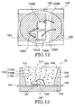
- Figs. 14A and 14B show such a typical conventional light emitting device.
- Fig. 14A is a plan view showing a configuration of the substantially part thereof, and
- Fig. 14B is a cross-sectional view thereof.
- the light emitting device shown here is of a so-called "surface mounting” type, including a package (resin stem) 800, semiconductor light emitting element 802 and sealing element 804 of a resin.
- the resin stem 800 has a structure molding a pair of leads 805, 806 shaped from lead frames with a resin portion 803 of a thermoplastic resin.
- the resin portion 803 has an opening 801, and the semiconductor light emitting element 802 is place therein. Then the semiconductor light emitting element 802 is sealed with an epoxy resin 804.
- the semiconductor light emitting element 802 is mounted on the lead 806.
- An electrode (not shown) of the semiconductor light emitting element 802 and the lead 805 are connected to each other by a wire 809.
- the semiconductor light emitting element 802 emits light, and the light is extracted from an emission surface 812 via the epoxy resin 804.
- those having two or more semiconductor elements common in emission wavelength are enhanced in output.
- Those having two or more semiconductor elements different in emission wavelength can provide mixed color, thereby to diversify the color representation.
- two complementary colors can produce white light.
- the light emitting device shown in Figs. 14A and 14B cannot provide a sufficient space for mounting the chip and for bonding the wire as well. If two chips are packed in the narrow opening by force, the optical axis of the light emitting element will largely offset from the center of the opening, and the intensity profile of the emitted light, i.e., luminous intensity property, will become asymmetrical. Then, the light emitting device cannot provide a uniform emission pattern required in applications such as the back light of a liquid crystal display.
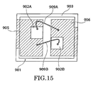
- Fig. 15 is a schematic diagram showing a plan-viewed configuration of a light emitting device prepared by the Inventor for trial toward the present invention.
- the light emitting device shown here has an approximately rectangular opening 901 formed in a resin portion 903, and chips 902A, 902B mounted on opposed leads 905, 906, respectively, at the bottom of the opening 901. Wires 909A, 909B extending from the chips 902A, 902B are connected to the opposed leads 906, 905, respectively.
- the fist problem is that a part of an adhesive extruding out upon mounting the chips 902A, 902B causes insufficient bonding of the wires 909A, 909B.
- pastes such as silver paste or solders such as gold-tin (AuSn) or gold-germanium (AuGe) solder is usually used.
- the second problem lies in that the illustrated rectangular shape of the opening 901 causes side walls of the resin portion 903 to be uniformly thin, and makes the mechanical strength insufficient. This problem becomes serious especially when a soft resin is used as the sealing element buried in the opening.
- a silicone resin used as the sealing element is advantageous for reducing the residual stress and thereby reducing cracks of the sealing element and breakage of the wire.
- the relatively soft silicone resin often fails to prevent an external lateral force to act on the chip and the wire. For example, upon picking up the light emitting device by grasping from its side surfaces for assembly and a test, the force actually acted upon the chip and the wire, and often deformed the wire.
- the third problem is that the illustrated rectangular shape of the opening 901 need a larger quantity of resin buried therein, and sometimes increases the resin stress.
- the resin filled in the opening 901 produces a stress upon curing, or thereafter upon an increase of decrease of the temperature.
- the degree of the stress depends on the buried quantity of the resin, and tends to increase as the buried quantity increases.
- the sealing resin filled in the illustrated rectangular opening 901 produced a large stress, and is liable to cause exfoliation of the chips 902A, 902B, and deformation or breakage of the wires 909A, 909B.
- a light emitting device comprising: a lead; a resin portion which buries at least a part of said lead; a first semiconductor light emitting element mounted on said lead in an opening formed in said resin portion; a semiconductor element mounted on said lead in said opening; and a wire connecting said first semiconductor light emitting element and said lead, said lead having a slit formed between a portion where said first semiconductor light emitting element is mounted and a portion where said wire is connected.
- a light emitting device comprising: a first lead; a second lead; a resin portion which buries at least a part of said first and second leads; a first semiconductor light emitting element mounted on said first lead in an opening formed in said resin portion; a semiconductor element mounted on said second lead in said opening; a first wire connecting said first semiconductor light emitting element and said second lead; and a second wire connecting said semiconductor element and said first lead, said first lead having a first slit formed between a portion where said first semiconductor light emitting element is mounted and a portion where said second wire is connected, and said second lead having a second slit formed between a portion where said semiconductor element is mounted and a portion where said first wire is connected.
- a light emitting device comprising: a first lead; a second lead; a resin portion which buries at least a part of said first and second leads; a first semiconductor light emitting element mounted on said first lead in an opening formed in said resin portion; a semiconductor element mounted on said first lead in said opening; a first wire connecting said first semiconductor light emitting element and said second lead; and a second wire connecting said semiconductor element and said second lead, said opening having a substantially elliptical or elongate-circular opening shape,said first semiconductor light emitting element and said semiconductor element being arranged along a longer axis or a shorter axis of said elliptical or elongate-circular opening.
- the "elongate-circle” means a shape connecting a pair of curved portions by a pair of substantially straight portions.
- the curved portions may be either regularly arc-shaped or irregularly arc-shaped.
- the "fluorescent element” may be any having a wavelength converting function, either inorganic or organic, including inorganic dyes having a wavelength converting function.
- nitride semiconductors include III-V compound semiconductors expressed by the chemical formula B x In y Al z Ga (1-x-y-z) N (0 ⁇ x ⁇ 1, 0 ⁇ y ⁇ 1, 0 ⁇ z ⁇ 1, 0 ⁇ x+y+z ⁇ 1), where each of x, y, and z is varied throughout its respective range, and further include mixed crystals containing not only N (nitrogen) but also phosphorus (P) and/or arsenic (As) in addition to N as group V elements.
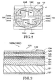
- Figs. 1A and 1B show schematic diagrams illustrating a configuration of the substantial part of a light emitting device according to the first embodiment of the invention, in which Fig. 1A is a plan view and Fig. 1B is a cross-sectional view taken along the A-A line of Fig. 1A.
- the light emitting device 1A shown here includes a resin stem 100, a semiconductor light emitting element 106A mounted on the resin stem 100, a protective Zener diode 106B and a sealing element 111 provided to embed them.
- the resin stem 100 includes leads 101, 102 shaped from a lead frame, and a resin portion 103 molded integrally with the leads 101, 102.
- the leads 101, 102 have opposed ends close to each other, and extend therefrom in the opposite directions to outside the resin portion 103.
- the resin portion 103 has formed an opening 105, and the semiconductor light emitting element 106A and the diode 106B are mounted at the bottom of the opening 105.
- the plan-viewed shape of the opening 105 is approximately elliptical or approximately elongate-circular as illustrated.
- the inner wall surface of the resin portion 103 surrounding the elements 106A, 106B inclines to face toward the light extraction direction to function as a reflective surface 104 for reflecting light.
- the lead 101 and the lead 102 are isolated. Near the distal end of the lead 101, a slit 101G is formed to divide it into the regions 101A and 101B. Similarly, near the distal end of the lead 102, a slit 102G is formed to divide it into the regions 102A and 102B.
- the light emitting element 106A is mounted in the region 101A with an adhesive such as silver (Ag) paste.
- the light emitting element 106B is mounted in the region 102B similarly with an adhesive 107 such as silver (Ag) paste.
- the wire 109A is connected to the opposed region 102A. From an electrode (not shown) formed on the diode 106B, the wire 109B is connected to the opposed region 101B.
- the slits 101G, 102G formed near distal ends of the leads 101, 102 separate each of them into the portion (101A, 102B) for mounting the chips 106A, 106B and the portion (101B, 102A) for bonding the wires 109A, 109B.
- This configuration keeps the portion for bonding the wire clean even when silver paste, for example, extrudes upon mounting the chip, and thereby eliminates defective bonding of wires.
- the invention employs a shape with a longer diameter and a shorter diameter such as an approximately elliptical shape or an approximately elongate-circular shape as the shape of the opening in lieu of an approximately circular shape as shown by a broken line in Fig. 1A, which has been used conventionally, it is possible to effectively increase the area of the opening 105 and thereby make an ample space for mounting two or more chips and bonding the wires.
- the approximately elliptical or elongate-circular shape of the opening according to the invention makes it easy to locate the light emitting element closest to the center of the opening.
- the use of the approximately elliptical or elongate-circular shape of the opening according to the invention also enables the corner portions 103C to be made thicker. As a result, the light emitting device maintains a sufficient mechanical strength, and it is prevented from deformation or wires and other kinds of damage even upon application of a lateral force during assembly or tests.
- the approximately elliptical or elongate-circular shape of the opening prevents an increase of the resin quantity filled inside and thereby prevents the resin stress.
- the resin stress increases as the quantity of resin filled as the sealing element 111 increases.
- the invention minimizes the increase of the resin quantity and simultaneously keeps an ample space for locating a plurality of chips. It results in eliminating the problems of exfoliation of chips, deformation or breakage of wires due to an increase of the resin stress.
- the invention enables mounting of a plurality of chips while maintaining the outer dimension of the light emitting device compact.
- the invention can improve the reliability.
- the device can realize emission of white and other various colors, which has been difficult to emit conventionally.
- the slits 101G, 102G formed in the leads 101, 102 facilitate corners of the lead patterns to be cognized inside the opening in the process of mounting chips or bonding wires. Therefore, the invention ensures more accurate mounting positions of the chips and more accurate bonding positions of the wires than conventional techniques.
- Fig. 2 is a plan view that schematically shows the first modification of the first embodiment.
- the same or equivalent components as those already explained with reference to Figs. 1A and 1B are commonly labeled, and their detailed explanation is omitted for simplicity.
- the light emitting device shown here includes two semiconductor light emitting elements 106, 106C on board.
- elements 106A, 106C reversed in conduction type may be used. That is, one of them may be configured n-side down while the other p-side down.
- the optical output of the light emitting device can be doubled.
- the light emitting device can provide light of a mixed color.
- white light can be realized by combining, for example, a blue light emitting element and a yellow light emitting element that are chromatically complementary.
- White light can be obtained also by combining a red light emitting element and a blue-green light emitting element.
- Fig. 3 is a cross-sectional view that schematically shows a semiconductor light emitting element made with a nitride compound semiconductor which can realize a strong emission in a wavelength range between ultraviolet through green.
- the light emitting element 106A (or 106C) includes a buffer layer 122, n-type contact layer 123, light emitting layer 124, p-type cladding layer 125 and p-type contact layer 126 sequentially stacked on a conductive substrate 121.
- the light emitting layer 124 may have a quantum well (QW) structure in which barrier layers and well layers are stacked alternately.
- QW quantum well
- the conductive substrate 121 may be made of, for example, an n-type GaN or SiC. Respective layers on the substrate may be made of, for example, III-V compound semiconductors, II-IV compound semiconductors, IV-VI compound semiconductors and other various materials.
- n-side electrode 127 is provided on the rear surface of the substrate 121.
- a translucent p-side electrode 128 made of a stacked structure including a nickel (Ni) layer and a gold (Au) layer of a thickness of several ten nanometers, and a bonding pad 129 of gold (Au) connected to the p-side electrode 128.
- Surface of the element is covered by a protective film 130 of SiO 2 .
- the emission wavelength can be adjusted in a wide range by adjusting the material and thickness of the light emitting layer.
- the embodiment shown here can realize various emission colors by using such semiconductor light emitting elements.
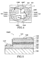
- Fig. 4 is a plan view that schematically shows the second specific example according to the first embodiment.
- the same or equivalent components as those already explained with reference to Figs. 1A through 3 are commonly labeled, and their detailed explanation is omitted for simplicity.
- the light emitting device shown here includes a protective diode 106B and a semiconductor light emitting element 106D.
- the light emitting element 106D is formed on an insulating substrate, and includes p -side and n -side electrodes (not shown) on the front surface. wires 109B, 109C extending from these electrodes are connected to the leads 101B, 102B, respectively.
- the protective diode 106B and the light emitting element 106D are connected in the opposite directions in parallel.
- Fig. 5 is a cross-sectional view that shows a structure of the semiconductor light emitting element 106D.
- the device shown here is made by stacking nitride compound semiconductor layers on an sapphire substrate 133. More specifically, sequentially stacked on the sapphire substrate 133 are a buffer layer 122, n-type contact layer 123, light emitting layer 124, p-type cladding layer 125 and p-type contact layer 126.
- the light emitting layer 124 may have a quantum well (QW) structure in which GaN barrier layers and InGaAlN well layers are stacked alternately.
- QW quantum well
- an n-side electrode 127 made of, for example; Ti/Al is formed on the n-type contact layer 123 exposed by selectively removing the multi-layered structure from its surface by etching.
- an n-side electrode 127 made of, for example; Ti/Al is formed on the p-type contact layer 126 .
- Surface of the element is covered by a protective film 130 of SiO 2 .
- the specific example shown in Fig. 4 can compactly accommodate both the semiconductor light emitting element 106D formed on the insulating substrate and the protective diode 106B in a limited space, and can reliably, easily bond the predetermined wires 109A through 109C. Moreover, since the chips and the wire bonding portion are isolated by the slits 101G, 102G, defective bonding by extrusion of the adhesive can be eliminated.
- Fig. 6 is a plan view that schematically shows the third modification example according to the first embodiment.
- the same or equivalent components as those already explained with reference to Figs. 1A through 4 are commonly labeled, and their detailed explanation is omitted for simplicity.
- the light emitting device shown here also includes the protective diode 106B and the semiconductor light emitting element 106D.
- the opening 105 is not elliptical but approximately elongate-circular.
- the "elongate circle” means a shape, like that of the opening 105 shown in Fig. 6, having a pair of opposed approximately arc-curved portions and connecting these curved portions by substantially straight portions.
- the curved portions need not be strictly arc-shaped. That is, the "approximately elongate-circle" pertains to a shape made up of a pair of curved portions connected by two substantially straight portions.
- the approximately elongate circle is advantageous for easier processing upon forming the opening 105 in the resin portion 103.
- the light emitting device can maintain a sufficient mechanical strength against a lateral stress or impulse.
- shapes of the distal ends of the pair of leads 101, 102 are asymmetric. That is, the portion 102B for mounting the light emitting element 106D on is formed to extend forward toward the center of the opening 105.
- the light emitting element 106D can be located in the center of the opening 105, and the intensity profile of the emitted light, i.e. the luminous intensity property can be approximated to a uniform or symmetric profile. It is also possible to enhance the luminance.
- “Locating in the center” herein means to locate any portion of the light emitting element 106D on the central axis of the opening 105.
- the specific example shown here may use the light emitting element 106A (or 106C) using a conductive substrate instead of the light emitting element 106D.
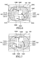
- Fig. 7 is a plan view that schematically shows the fourth specific example according to the first embodiment.
- the same or equivalent components as those already explained with reference to Figs. 1A through 6 are commonly labeled, and their detailed explanation is omitted for simplicity.
- the light emitting device shown here also includes the protective diode 106B and the semiconductor light emitting element 106D.
- the opposed distal ends of the pair of leads 101, 102 are aligned straight instead of being offset. Then the diode 106B and the light emitting element 106D are mounted at diagonal positions.
- the light emitting element 106D is formed to be closer to the center of the opening 105 than the diode 106B. Locating the optical axis closer to the center of the opening 105 ensures a more uniform luminous intensity property.
- Fig. 8 is a plan view that schematically shows the fifth specific example according to the first embodiment.
- the same or equivalent components as those already explained with reference to Figs. 1A through 7 are commonly labeled, and their detailed explanation is omitted for simplicity.
- the light emitting device shown here also includes the protective diode 106B and the semiconductor light emitting element 106D, and the opposed distal ends of the pair of leads 101, 102 are aligned straight instead of being offset.
- the slits 101G, 102G are formed to be offset from each other. This configuration can also locate the light emitting element 106D close to the center of the opening 105.
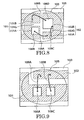
- Fig. 9 is a plan view that schematically shows the specific example according to the second embodiment.
- the same or equivalent components as those already explained with reference to Figs. 1A through 8 are commonly labeled, and their detailed explanation is omitted for simplicity.
- two chips are mounted on a common lead, and they are aligned along the lengthwise direction of the opening 105 having an approximately elliptical or elongate-circular shape.
- the semiconductor light emitting elements 106A, 106C are mounted side by side on the lead 101, and the wires 109A, 109B are connected to the lead 102 in the opposed position with respect to the shorter axis of the opening 105.
- This arrangement of a plurality of chips along the longer axis, i.e. length wise direction, of the approximately elliptical or elongate-circular opening 105 is advantageous for effective use of the limited space.
- Fig. 10 is a plan view that schematically shows the modification, of the second embodiment.
- the same or equivalent components as those already explained with reference to Figs. 1A through 9 are commonly labeled, and their detailed explanation is omitted for simplicity.
- a second wire 109C from the light emitting element 106D it is necessary to connect a second wire 109C from the light emitting element 106D to the lead 101.
- a slit 101G is formed in the lead 101, and the wire 109C is connected across the slit 101G. In this manner, the bonding region can be isolated from extrusion of the adhesive upon mounting the light emitting element 106D and the diode 106B.
- Fig. 11 is a plan view that schematically shows the twelfth specific example according to the first embodiment.
- the same or equivalent components as those already explained with reference to Figs. 1A through 10 are commonly labeled, and their detailed explanation is omitted for simplicity.
- two chips are mounted on a common lead. These two chips, however, are disposed along the shorter axis direction of the approximately elliptical or elongate-circular opening 15. Then the wires 109A, 109B are connected to the lead 102 in the opposed position with respect to the shorter axis of the opening 105.
- This arrangement of a plurality of chips along the shorter axis of the approximately elliptical or elongate-circular opening 105 is also advantageous for effective use of the limited space.
- Fig. 12 is a plan view that schematically shows the modification of the third embodiment.
- the same or equivalent components as those already explained with reference to Figs. 1A through 11 are commonly labeled, and their detailed explanation is omitted for simplicity.
- a second wire 109C from the light emitting element 106D it is necessary to connect a second wire 109C from the light emitting element 106D to the lead 101.
- a slit 101G is formed in the lead 101, and the wire 109C is connected across the slit 101G. In this manner, the bonding region can be isolated from extrusion of the adhesive upon mounting the light emitting element 106D and the diode 106B.
- Fig. 13 is a cross-sectional view that schematically shows a configuration of the substantial part of a light emitting device according to the instant embodiment.
- the same or equivalent components as those already explained with reference to Figs. 1A through 12 are commonly labeled, and their detailed explanation is omitted for simplicity.
- the light emitting element 106 is connected in parallel with a protective diode, not shown.
- the layout pattern of these chips and the leads 101, 102 may be any of those explained with reference to Figs. 1A through 12.
- the opening 105 in form of an approximate ellipse or flattened circle formed in the resin portion 103 is buried by the sealing element 111 containing the fluorescent element 110.
- the sealing element 111 may be provided to bury a part of the opening 105 in lieu of the manner shown here.
- the fluorescent element 110 contained in the sealing element 111 absorbs primary light emitted from the light emitting element 106 and releases light of a predetermined wavelength.
- the light emitting element 106 may be configured to emit ultraviolet rays, i.e. light having a peak wavelength shorter than 400 nm, and may be combined with a fluorescent element that absorbs this short wavelength light and releases light of a predetermined wavelength.
- a fluorescent element that absorbs this short wavelength light and releases light of a predetermined wavelength.
- white light can be obtained as their mixture.
- the sealing element 111 is preferably made of a silicone resin instead of an epoxy resin used in the conventional devices.
- Epoxy resins deteriorate when exposed to short-wavelength light, and although originally transparent, they change in color through yellow, liver to black finally, and result in a serious decrease of the light extraction efficiency. silicone resins are substantially free from such deterioration.
- silicon resin any resin having as its skeleton a structure in which silicon atoms having organic radicals such as alkyl radicals or aryl radicals are alternately connected to oxygen atoms. Needless to say, those containing additive elements added to such skeletons are also included in “silicone resins”.
- a light source of a short wavelength is preferably used.
- the light source using nitride semiconductor as explained with reference to Fig. 3 and Fig. 5.
- a diode like a Zener diode
- the invention can reliably cope with this requirement.
- the invention makes it possible to efficiently place a plurality of chips and well isolate the wire bonding region, thereby to eliminate defective bonding.
- the invention can realize a high-performance light emitting device combining the semiconductor light emitting element 106 using a nitride semiconductor with the fluorescent element 110 as shown in Fig. 13.
- combination of chips mounted on the light emitting device is not limited to that illustrated, but combination of a light emitting element 106A (or 106C) and a diode 106B, combination of two or more light emitting elements 106A (or 106C), and combination of a light emitting element 106A (or 106C) and a light emitting element 106D are also acceptable.
- the number of chips mounted in the opening is not limited to two, but three or more chips can be mounted as well.
- the shape of the opening 105 may be either approximately elliptical or flattened-circular.
- the light emitting elements 106A, 106C, 106D used in the invention are not limited to those using a nitride semiconductor, but those using GaAs/AlGaAs compounds, InP/InGaAs compounds, InGaAlP compounds, ZeSe compounds, ZnS compounds and other various materials can be similarly used as well. This is the case also for the diode 106B.
Landscapes
- Led Device Packages (AREA)
- Semiconductor Lasers (AREA)
- Led Devices (AREA)
Applications Claiming Priority (2)
| Application Number | Priority Date | Filing Date | Title |
|---|---|---|---|
| JP2001110674A JP2002314138A (ja) | 2001-04-09 | 2001-04-09 | 発光装置 |
| JP2001110674 | 2001-04-09 |
Publications (2)
| Publication Number | Publication Date |
|---|---|
| EP1249876A2 true EP1249876A2 (de) | 2002-10-16 |
| EP1249876A3 EP1249876A3 (de) | 2008-06-04 |
Family
ID=18962397
Family Applications (1)
| Application Number | Title | Priority Date | Filing Date |
|---|---|---|---|
| EP20020007381 Withdrawn EP1249876A3 (de) | 2001-04-09 | 2002-04-09 | Lichtemittierende Vorrichtung |
Country Status (5)
| Country | Link |
|---|---|
| US (2) | US7242032B2 (de) |
| EP (1) | EP1249876A3 (de) |
| JP (1) | JP2002314138A (de) |
| CN (1) | CN1233045C (de) |
| TW (1) | TW541720B (de) |
Cited By (5)
| Publication number | Priority date | Publication date | Assignee | Title |
|---|---|---|---|---|
| ES2333756A1 (es) * | 2006-11-29 | 2010-02-26 | Higher Way Electronic Co., Ltd. | Iluminador alimentado por energia solar. |
| WO2011129383A1 (ja) * | 2010-04-15 | 2011-10-20 | シチズン電子株式会社 | 発光装置 |
| CN102130113B (zh) * | 2006-04-27 | 2013-01-23 | 克里公司 | 用于半导体发光器件封装的子基板和包括其的半导体发光器件封装 |
| EP2325898A4 (de) * | 2008-08-26 | 2013-12-25 | Dingguo Pan | Led-mehrchip-bondchip und den bondchip haltender lichtstreifen |
| EP1925036B1 (de) * | 2005-09-13 | 2016-04-13 | Toyoda Gosei Co., Ltd. | Lichtemittierende nitridhalbleitervorrichtung und deren herstellungsverfahren |
Families Citing this family (71)
| Publication number | Priority date | Publication date | Assignee | Title |
|---|---|---|---|---|
| US10309587B2 (en) * | 2002-08-30 | 2019-06-04 | GE Lighting Solutions, LLC | Light emitting diode component |
| KR100533635B1 (ko) | 2003-11-20 | 2005-12-06 | 삼성전기주식회사 | Led 패키지 |
| JP4632677B2 (ja) * | 2004-03-11 | 2011-02-16 | オリンパス株式会社 | 内視鏡装置 |
| WO2006036559A1 (en) * | 2004-09-27 | 2006-04-06 | Idc, Llc | Method and device for manipulating color in a display |
| JP4796293B2 (ja) * | 2004-11-04 | 2011-10-19 | 株式会社 日立ディスプレイズ | 照明装置の製造方法 |
| JP5373244B2 (ja) * | 2005-02-24 | 2013-12-18 | 株式会社朝日ラバー | 発光ダイオード用レンズ部品及び発光ダイオード光源装置 |
| JP2006253215A (ja) * | 2005-03-08 | 2006-09-21 | Sharp Corp | 発光装置 |
| JP2007005748A (ja) * | 2005-06-23 | 2007-01-11 | Lite-On Technology Corp | 光電子半導体素子 |
| CN100479153C (zh) * | 2005-07-19 | 2009-04-15 | 光宝科技股份有限公司 | 具有高发光效率的光电半导体元件 |
| DE102005041064B4 (de) * | 2005-08-30 | 2023-01-19 | OSRAM Opto Semiconductors Gesellschaft mit beschränkter Haftung | Oberflächenmontierbares optoelektronisches Bauelement und Verfahren zu dessen Herstellung |
| US20070080360A1 (en) * | 2005-10-06 | 2007-04-12 | Url Mirsky | Microelectronic interconnect substrate and packaging techniques |
| JP4835104B2 (ja) * | 2005-10-24 | 2011-12-14 | 日亜化学工業株式会社 | 半導体発光装置 |
| KR100675204B1 (ko) * | 2006-02-07 | 2007-01-29 | 삼성전기주식회사 | 발광 다이오드 패키지 |
| JP4882476B2 (ja) * | 2006-04-17 | 2012-02-22 | 日亜化学工業株式会社 | 半導体装置及びその製造方法 |
| JP4830768B2 (ja) * | 2006-05-10 | 2011-12-07 | 日亜化学工業株式会社 | 半導体発光装置及び半導体発光装置の製造方法 |
| JP4205135B2 (ja) | 2007-03-13 | 2009-01-07 | シャープ株式会社 | 半導体発光装置、半導体発光装置用多連リードフレーム |
| US7514724B2 (en) * | 2007-03-23 | 2009-04-07 | Avago Technologies Ecbu Ip (Singapore) Pte. Ltd. | Solid state light source having a variable number of dies |
| US7964888B2 (en) * | 2007-04-18 | 2011-06-21 | Cree, Inc. | Semiconductor light emitting device packages and methods |
| US20080290359A1 (en) | 2007-04-23 | 2008-11-27 | Samsung Electro-Mechanics Co., Ltd. | Light emitting device and manufacturing method of the same |
| KR100990637B1 (ko) * | 2007-04-23 | 2010-10-29 | 삼성엘이디 주식회사 | 발광장치 및 그 제조방법 |
| JP2008300573A (ja) * | 2007-05-30 | 2008-12-11 | Toshiba Corp | 発光装置 |
| JP5416975B2 (ja) | 2008-03-11 | 2014-02-12 | ローム株式会社 | 半導体発光装置 |
| TWI488329B (zh) | 2008-05-15 | 2015-06-11 | 億光電子工業股份有限公司 | 線路基板與發光二極體封裝 |
| CN101582402B (zh) * | 2008-05-16 | 2012-09-19 | 亿光电子工业股份有限公司 | 线路基板 |
| CN102142423B (zh) * | 2008-05-16 | 2014-11-26 | 亿光电子工业股份有限公司 | 线路基板与发光二极管封装 |
| JP5217800B2 (ja) | 2008-09-03 | 2013-06-19 | 日亜化学工業株式会社 | 発光装置、樹脂パッケージ、樹脂成形体並びにこれらの製造方法 |
| TWI384591B (zh) * | 2008-11-17 | 2013-02-01 | 億光電子工業股份有限公司 | 發光二極體電路板 |
| TWI401896B (zh) * | 2009-03-03 | 2013-07-11 | Everlight Electronics Co Ltd | 光遮斷器 |
| JP2011071265A (ja) | 2009-09-25 | 2011-04-07 | Toshiba Corp | 発光装置 |
| JP5446843B2 (ja) * | 2009-12-24 | 2014-03-19 | 豊田合成株式会社 | Led発光装置 |
| JP5506313B2 (ja) * | 2009-09-30 | 2014-05-28 | スタンレー電気株式会社 | 車両ヘッドライト用発光ダイオード光源 |
| TW201128812A (en) | 2009-12-01 | 2011-08-16 | Lg Innotek Co Ltd | Light emitting device |
| JP4764519B1 (ja) * | 2010-01-29 | 2011-09-07 | 株式会社東芝 | Ledパッケージ |
| WO2011133228A2 (en) | 2010-04-23 | 2011-10-27 | Pixelligent Technologies, Llc | Synthesis, capping and dispersion of nanocrystals |
| JP5528900B2 (ja) * | 2010-04-30 | 2014-06-25 | ローム株式会社 | 発光素子モジュール |
| TWI561770B (en) * | 2010-04-30 | 2016-12-11 | Samsung Electronics Co Ltd | Light emitting device package, light source module, backlight unit, display apparatus, television set, and illumination apparatus |
| US8848294B2 (en) | 2010-05-20 | 2014-09-30 | Qualcomm Mems Technologies, Inc. | Method and structure capable of changing color saturation |
| KR101103674B1 (ko) | 2010-06-01 | 2012-01-11 | 엘지이노텍 주식회사 | 발광 소자 |
| KR101859149B1 (ko) | 2011-04-14 | 2018-05-17 | 엘지이노텍 주식회사 | 발광 소자 패키지 |
| KR101705700B1 (ko) * | 2010-07-01 | 2017-02-10 | 엘지이노텍 주식회사 | 발광 소자 |
| EP3190083B1 (de) | 2010-10-27 | 2020-08-26 | Pixelligent Technologies, LLC | Synthese, abdeckung und dispergierung von nanokristallen |
| US20120112237A1 (en) * | 2010-11-05 | 2012-05-10 | Shenzhen China Star Optoelectronics Technology Co. Ltd. | Led package structure |
| JP2012114286A (ja) * | 2010-11-25 | 2012-06-14 | Toshiba Corp | Ledパッケージ |
| US10234545B2 (en) * | 2010-12-01 | 2019-03-19 | Microsoft Technology Licensing, Llc | Light source module |
| JP5781801B2 (ja) * | 2011-03-29 | 2015-09-24 | シチズン電子株式会社 | Led発光装置 |
| KR101832306B1 (ko) * | 2011-05-30 | 2018-02-26 | 엘지이노텍 주식회사 | 발광소자 패키지 |
| KR20120137865A (ko) * | 2011-06-13 | 2012-12-24 | 엘지이노텍 주식회사 | 발광소자 및 발광소자 패키지 |
| WO2013036481A2 (en) * | 2011-09-06 | 2013-03-14 | Cree, Inc. | Light emitter packages and devices having improved wire bonding and related methods |
| US9359689B2 (en) | 2011-10-26 | 2016-06-07 | Pixelligent Technologies, Llc | Synthesis, capping and dispersion of nanocrystals |
| DE102011056708A1 (de) * | 2011-12-20 | 2013-06-20 | Osram Opto Semiconductors Gmbh | Verfahren zur Herstellung von optoelektronischen Halbleiterbauteilen, Leiterrahmenverbund und optoelektronisches Halbleiterbauteil |
| DE102011056700A1 (de) * | 2011-12-20 | 2013-06-20 | Osram Opto Semiconductors Gmbh | Verfahren zur Herstellung von optoelektronischen Halbleiterbauteilen, Leiterrahmenverbund und optoelektronisches Halbleiterbauteil |
| TW201411894A (zh) * | 2012-09-10 | 2014-03-16 | Walsin Lihwa Corp | 發光裝置 |
| JP2016115688A (ja) * | 2013-04-05 | 2016-06-23 | パナソニック株式会社 | 発光装置 |
| CN105826290A (zh) * | 2013-07-12 | 2016-08-03 | 苏州固锝电子股份有限公司 | 低功耗半导体整流器件 |
| US9166131B2 (en) * | 2013-07-17 | 2015-10-20 | Tai-Yin Huang | Composite LED package and its application to light tubes |
| JP2015119096A (ja) * | 2013-12-19 | 2015-06-25 | 株式会社タムラ製作所 | 発光装置 |
| JP2015126137A (ja) * | 2013-12-26 | 2015-07-06 | アピックヤマダ株式会社 | リードフレーム、ledパッケージ用基板、リフレクタ部材、ledパッケージ、発光装置、発光システム、並びに、ledパッケージ用基板及びledパッケージの製造方法 |
| US10257932B2 (en) | 2016-02-16 | 2019-04-09 | Microsoft Technology Licensing, Llc. | Laser diode chip on printed circuit board |
| US11677059B2 (en) | 2017-04-26 | 2023-06-13 | Samsung Electronics Co., Ltd. | Light-emitting device package including a lead frame |
| KR102335216B1 (ko) | 2017-04-26 | 2021-12-03 | 삼성전자 주식회사 | 발광소자 패키지 |
| US20180323239A1 (en) * | 2017-05-03 | 2018-11-08 | Innolux Corporation | Display device |
| JP7004397B2 (ja) * | 2017-06-09 | 2022-01-21 | ローム株式会社 | 光学装置 |
| JP6822442B2 (ja) * | 2018-03-01 | 2021-01-27 | 日亜化学工業株式会社 | 発光装置およびその製造方法 |
| JP6797861B2 (ja) * | 2018-05-09 | 2020-12-09 | 日亜化学工業株式会社 | 発光装置の製造方法及び発光装置 |
| JP7128410B2 (ja) * | 2018-07-30 | 2022-08-31 | 日亜化学工業株式会社 | 光源装置 |
| JP6809518B2 (ja) * | 2018-08-28 | 2021-01-06 | 日亜化学工業株式会社 | 樹脂成形体及び表面実装型発光装置並びにそれらの製造方法 |
| JP6842485B2 (ja) * | 2019-03-04 | 2021-03-17 | ローム株式会社 | Ledモジュール |
| DE102020107409B4 (de) * | 2020-03-18 | 2023-11-02 | OSRAM Opto Semiconductors Gesellschaft mit beschränkter Haftung | Gehäuse für ein optoelektronisches halbleiterbauelement und optoelektronisches halbleiterbauelement |
| JP7252503B2 (ja) * | 2020-04-09 | 2023-04-05 | 日亜化学工業株式会社 | 発光装置の製造方法及び発光装置 |
| CN114649447A (zh) * | 2020-12-18 | 2022-06-21 | 日亚化学工业株式会社 | 发光装置的制造方法及发光装置 |
| JP7389363B2 (ja) * | 2021-05-26 | 2023-11-30 | 日亜化学工業株式会社 | 発光装置 |
Citations (5)
| Publication number | Priority date | Publication date | Assignee | Title |
|---|---|---|---|---|
| JPH08162678A (ja) | 1994-11-30 | 1996-06-21 | Iwasaki Electric Co Ltd | 発光ダイオード及び発光ダイオードドットマトリックス |
| EP0838866A2 (de) | 1996-10-28 | 1998-04-29 | General Electric Company | Weisslichtquelle mit lichtemittierenden Dioden |
| EP0854523A2 (de) | 1997-01-15 | 1998-07-22 | Toshiba Corporation | Lichtemittierende Halbleitervorrichtung und Herstellungsverfahren |
| US6054716A (en) | 1997-01-10 | 2000-04-25 | Rohm Co., Ltd. | Semiconductor light emitting device having a protecting device |
| WO2001013473A1 (de) | 1999-08-16 | 2001-02-22 | Tyco Electronics Logistics Ag | Geschirmter elektrischer steckverbinder |
Family Cites Families (37)
| Publication number | Priority date | Publication date | Assignee | Title |
|---|---|---|---|---|
| GB1557685A (en) * | 1976-02-02 | 1979-12-12 | Fairchild Camera Instr Co | Optically coupled isolator device |
| JPS5429653A (en) | 1977-08-10 | 1979-03-05 | Tomoegawa Paper Co Ltd | Heat sensitive recording medium |
| JPS57162670A (en) | 1981-03-31 | 1982-10-06 | Tetsuhiko Inoue | Forming method for sticking film |
| JPH0638514B2 (ja) * | 1985-11-21 | 1994-05-18 | 日本電気株式会社 | フオトインタラプタ |
| US4794431A (en) * | 1986-04-21 | 1988-12-27 | International Rectifier Corporation | Package for photoactivated semiconductor device |
| JPH01146376A (ja) | 1987-12-02 | 1989-06-08 | Stanley Electric Co Ltd | チップled |
| JPH01154804A (ja) | 1987-12-10 | 1989-06-16 | Kobe Steel Ltd | 箔圧延機 |
| US4890383A (en) * | 1988-01-15 | 1990-01-02 | Simens Corporate Research & Support, Inc. | Method for producing displays and modular components |
| US4843280A (en) | 1988-01-15 | 1989-06-27 | Siemens Corporate Research & Support, Inc. | A modular surface mount component for an electrical device or led's |
| JPH0292927A (ja) | 1988-09-30 | 1990-04-03 | Chisso Corp | 遊離ε−ポリリシンの製造法 |
| JPH0292927U (de) * | 1989-01-11 | 1990-07-24 | ||
| JPH0427175A (ja) * | 1990-05-22 | 1992-01-30 | Iwasaki Electric Co Ltd | 多色発光ダイオード |
| US5173810A (en) * | 1991-08-21 | 1992-12-22 | Aisens Co., Ltd. | Light transmitting lens for use with a photoelectric sensor |
| JPH0559863U (ja) * | 1992-01-21 | 1993-08-06 | サンケン電気株式会社 | 半導体発光装置 |
| JP2809951B2 (ja) * | 1992-12-17 | 1998-10-15 | 株式会社東芝 | 半導体発光装置とその製造方法 |
| JP3420612B2 (ja) * | 1993-06-25 | 2003-06-30 | 株式会社東芝 | Ledランプ |
| US5489800A (en) * | 1994-08-31 | 1996-02-06 | Motorola, Inc. | Dual channel small outline optocoupler package and method thereof |
| US5896010A (en) * | 1995-09-29 | 1999-04-20 | Ford Motor Company | System for controlling lighting in an illuminating indicating device |
| TW383508B (en) | 1996-07-29 | 2000-03-01 | Nichia Kagaku Kogyo Kk | Light emitting device and display |
| JP4316019B2 (ja) * | 1996-10-01 | 2009-08-19 | 株式会社東芝 | 半導体装置及び半導体装置製造方法 |
| JP3559435B2 (ja) * | 1997-01-10 | 2004-09-02 | ローム株式会社 | 半導体発光素子 |
| JP3673621B2 (ja) * | 1997-07-30 | 2005-07-20 | ローム株式会社 | チップ型発光素子 |
| JP3492178B2 (ja) * | 1997-01-15 | 2004-02-03 | 株式会社東芝 | 半導体発光装置及びその製造方法 |
| EP1959506A2 (de) * | 1997-01-31 | 2008-08-20 | Matsushita Electric Industrial Co., Ltd. | Herstellungsverfahren für eine lichtemittierende Halbleitervorrichtung |
| JPH10247748A (ja) * | 1997-03-03 | 1998-09-14 | Omron Corp | 発光素子及び当該発光素子を用いた面光源装置 |
| US6340824B1 (en) * | 1997-09-01 | 2002-01-22 | Kabushiki Kaisha Toshiba | Semiconductor light emitting device including a fluorescent material |
| US6147367A (en) * | 1997-12-10 | 2000-11-14 | Industrial Technology Research Institute | Packaging design for light emitting diode |
| JP3541709B2 (ja) * | 1998-02-17 | 2004-07-14 | 日亜化学工業株式会社 | 発光ダイオードの形成方法 |
| JPH10260645A (ja) * | 1998-04-20 | 1998-09-29 | Toshiba Corp | Ledランプ |
| JP3217322B2 (ja) * | 1999-02-18 | 2001-10-09 | 日亜化学工業株式会社 | チップ部品型発光素子 |
| JP3798195B2 (ja) * | 1999-08-12 | 2006-07-19 | ローム株式会社 | チップ型発光装置 |
| JP3833019B2 (ja) * | 1999-08-31 | 2006-10-11 | 日亜化学工業株式会社 | 発光ダイオード |
| EP1113506A3 (de) * | 1999-12-28 | 2005-03-16 | Toyoda Gosei Co., Ltd. | Lichtemittierende Diode |
| JP3644927B2 (ja) * | 2000-03-17 | 2005-05-11 | 松下電器産業株式会社 | 面発光装置 |
| JP2002314139A (ja) * | 2001-04-09 | 2002-10-25 | Toshiba Corp | 発光装置 |
| JP2002314143A (ja) * | 2001-04-09 | 2002-10-25 | Toshiba Corp | 発光装置 |
| JP4101468B2 (ja) * | 2001-04-09 | 2008-06-18 | 豊田合成株式会社 | 発光装置の製造方法 |
-
2001
- 2001-04-09 JP JP2001110674A patent/JP2002314138A/ja active Pending
-
2002
- 2002-04-04 TW TW091106881A patent/TW541720B/zh not_active IP Right Cessation
- 2002-04-09 EP EP20020007381 patent/EP1249876A3/de not_active Withdrawn
- 2002-04-09 US US10/119,524 patent/US7242032B2/en not_active Expired - Lifetime
- 2002-04-09 CN CNB021059020A patent/CN1233045C/zh not_active Expired - Fee Related
-
2006
- 2006-06-30 US US11/478,793 patent/US7719023B2/en not_active Expired - Fee Related
Patent Citations (5)
| Publication number | Priority date | Publication date | Assignee | Title |
|---|---|---|---|---|
| JPH08162678A (ja) | 1994-11-30 | 1996-06-21 | Iwasaki Electric Co Ltd | 発光ダイオード及び発光ダイオードドットマトリックス |
| EP0838866A2 (de) | 1996-10-28 | 1998-04-29 | General Electric Company | Weisslichtquelle mit lichtemittierenden Dioden |
| US6054716A (en) | 1997-01-10 | 2000-04-25 | Rohm Co., Ltd. | Semiconductor light emitting device having a protecting device |
| EP0854523A2 (de) | 1997-01-15 | 1998-07-22 | Toshiba Corporation | Lichtemittierende Halbleitervorrichtung und Herstellungsverfahren |
| WO2001013473A1 (de) | 1999-08-16 | 2001-02-22 | Tyco Electronics Logistics Ag | Geschirmter elektrischer steckverbinder |
Cited By (9)
| Publication number | Priority date | Publication date | Assignee | Title |
|---|---|---|---|---|
| EP1925036B1 (de) * | 2005-09-13 | 2016-04-13 | Toyoda Gosei Co., Ltd. | Lichtemittierende nitridhalbleitervorrichtung und deren herstellungsverfahren |
| CN102130113B (zh) * | 2006-04-27 | 2013-01-23 | 克里公司 | 用于半导体发光器件封装的子基板和包括其的半导体发光器件封装 |
| US8378374B2 (en) | 2006-04-27 | 2013-02-19 | Cree, Inc. | Semiconductor light emitting device packages including submounts |
| ES2333756A1 (es) * | 2006-11-29 | 2010-02-26 | Higher Way Electronic Co., Ltd. | Iluminador alimentado por energia solar. |
| EP2325898A4 (de) * | 2008-08-26 | 2013-12-25 | Dingguo Pan | Led-mehrchip-bondchip und den bondchip haltender lichtstreifen |
| WO2011129383A1 (ja) * | 2010-04-15 | 2011-10-20 | シチズン電子株式会社 | 発光装置 |
| US9006759B2 (en) | 2010-04-15 | 2015-04-14 | Citizen Electronics Co., Ltd. | Light-emitting device |
| JP5749709B2 (ja) * | 2010-04-15 | 2015-07-15 | シチズン電子株式会社 | 発光装置 |
| US9224720B2 (en) | 2010-04-15 | 2015-12-29 | Citizen Electronics Co., Ltd. | Light-emitting device including light-emitting diode element that is mounted on outer portion of electrode |
Also Published As
| Publication number | Publication date |
|---|---|
| US7719023B2 (en) | 2010-05-18 |
| US7242032B2 (en) | 2007-07-10 |
| EP1249876A3 (de) | 2008-06-04 |
| US20060249746A1 (en) | 2006-11-09 |
| CN1233045C (zh) | 2005-12-21 |
| US20020185649A1 (en) | 2002-12-12 |
| JP2002314138A (ja) | 2002-10-25 |
| TW541720B (en) | 2003-07-11 |
| CN1380702A (zh) | 2002-11-20 |
Similar Documents
| Publication | Publication Date | Title |
|---|---|---|
| US7719023B2 (en) | Light emitting device | |
| EP1249873B1 (de) | Lichtemittierende Vorrichtung | |
| US6747293B2 (en) | Light emitting device | |
| KR101602977B1 (ko) | 발광 장치 | |
| KR100853064B1 (ko) | 복합발광소자 | |
| CN101030617B (zh) | 发光器件封装及其制造方法 | |
| US5557115A (en) | Light emitting semiconductor device with sub-mount | |
| JP6796936B2 (ja) | 発光素子及びこれを備えたライトユニット | |
| US8742447B2 (en) | Light emitting device, light emitting device package and lighting system | |
| US11508701B2 (en) | Light emitting device | |
| JP4984824B2 (ja) | 発光装置 | |
| KR101813495B1 (ko) | 발광소자 패키지 | |
| US10101518B2 (en) | Integrated back light unit | |
| JP3228321B2 (ja) | チップタイプled | |
| JP5032747B2 (ja) | 半導体装置 | |
| CN106571418A (zh) | 半导体发光装置 | |
| JP2001217461A (ja) | 複合発光素子 | |
| JP2006222382A5 (de) | ||
| KR101946244B1 (ko) | 반도체 발광소자 | |
| KR100447029B1 (ko) | 반도체 엘이디 소자 및 그 제조 방법 | |
| KR20130060638A (ko) | 발광 소자, 이를 포함하는 발광 소자 패키지, 및 이를 포함하는 조명 시스템 |
Legal Events
| Date | Code | Title | Description |
|---|---|---|---|
| PUAI | Public reference made under article 153(3) epc to a published international application that has entered the european phase |
Free format text: ORIGINAL CODE: 0009012 |
|
| 17P | Request for examination filed |
Effective date: 20020409 |
|
| AK | Designated contracting states |
Kind code of ref document: A2 Designated state(s): AT BE CH CY DE DK ES FI FR GB GR IE IT LI LU MC NL PT SE TR |
|
| AX | Request for extension of the european patent |
Free format text: AL;LT;LV;MK;RO;SI |
|
| PUAL | Search report despatched |
Free format text: ORIGINAL CODE: 0009013 |
|
| AK | Designated contracting states |
Kind code of ref document: A3 Designated state(s): AT BE CH CY DE DK ES FI FR GB GR IE IT LI LU MC NL PT SE TR |
|
| AX | Request for extension of the european patent |
Extension state: AL LT LV MK RO SI |
|
| AKX | Designation fees paid |
Designated state(s): DE FR GB |
|
| 17Q | First examination report despatched |
Effective date: 20090204 |
|
| STAA | Information on the status of an ep patent application or granted ep patent |
Free format text: STATUS: THE APPLICATION IS DEEMED TO BE WITHDRAWN |
|
| 18D | Application deemed to be withdrawn |
Effective date: 20150731 |