EP1278328A2 - Modem avec dispositif de commande de gain - Google Patents
Modem avec dispositif de commande de gain Download PDFInfo
- Publication number
- EP1278328A2 EP1278328A2 EP02010768A EP02010768A EP1278328A2 EP 1278328 A2 EP1278328 A2 EP 1278328A2 EP 02010768 A EP02010768 A EP 02010768A EP 02010768 A EP02010768 A EP 02010768A EP 1278328 A2 EP1278328 A2 EP 1278328A2
- Authority
- EP
- European Patent Office
- Prior art keywords
- analog signal
- gain control
- reception analog
- maximum
- energy amount
- Prior art date
- Legal status (The legal status is an assumption and is not a legal conclusion. Google has not performed a legal analysis and makes no representation as to the accuracy of the status listed.)
- Granted
Links
Images


Classifications
-
- H—ELECTRICITY
- H04—ELECTRIC COMMUNICATION TECHNIQUE
- H04L—TRANSMISSION OF DIGITAL INFORMATION, e.g. TELEGRAPHIC COMMUNICATION
- H04L27/00—Modulated-carrier systems
- H04L27/26—Systems using multi-frequency codes
- H04L27/2601—Multicarrier modulation systems
- H04L27/2647—Arrangements specific to the receiver only
Definitions
- This invention relates to a gain control apparatus that performs a gain control of signal energy attached to each carrier, in communication using multi-carrier method, and a modem apparatus that is provided with the gain control apparatus.
- DMT Discrete Multi Tone
- DMT method is a multi-carrier modulating/demodulating method that employs multiple carriers (sub carriers) with different frequencies.
- Signals in communication using xDSL modems can be degraded because of factors such as line conditions . Due to such degradation of signals, signals are undetectable at the receiver side. Therefore, a gain control is used for the degradation of signals, to amplify signal energy.
- a gain control is performed by controlling the signal energy of a single carrier so that it will not be amplified to exceed an upper limit of the gain, thereby preventing a overflow.
- an ADSL modem that handles multi-carrier communication, even if a gain control is performed for one carrier so that its signal energy will not overflow, signal energy of other carriers can overflow. Thus, an appropriate gain control has not been available.
- the present invention is provided in view of above-described problems.
- the object of the invention is to provide a gain control apparatus that can appropriately perform a gain control of signal energy in multi-carrier communication, and a modem apparatus that is provided with the gain control apparatus.
- a maximum carrier energy amount is searched for, among energy amounts of multiple carriers comprising REVERB signals adhering to G. 992. 1 (G. DMT) or G. 992. 2 (G. Lite) of ITU-T standards.
- a gain control is performed to bring the energy amount to a target energy level, and at the same time, the same gain control for the carrier with the maximum energy amount is also performed for other carrier energy amounts across the board.
- Fig. 1 is a block diagram illustrating a configuration of a gain control apparatus according to the embodiment of the present invention.
- a gain controller 101 functions as an adjustor for signal energy that is given to each carrier of multi carriers. Specifically, the gain controller 101 performs a gain control for signal energy that is input from a public line (PSTN), via an interface, or output to the PSTN. The gain control by the gain controller 101 is performed according to a gain control amount given by a main controller (later described).
- PSTN public line
- the object is to perform a gain control especially for signal energy that is input from the PSTN, and to appropriately handle input signals. Therefore, the gain controller 101 performs a special gain control upon a signal input.
- the gain controller 101 performs a general process, e.g., a process for raising energy amount of output signal energy to a predetermined level.
- An A/D (D/A) converter 102 performs a digital/analog conversion process (D/A conversion process) of an output signal toward the PSTN, and performs an analog/digital conversion process (A/D conversion process ) for an input signal from the PSTN.
- D/A conversion process digital/analog conversion process
- A/D conversion process analog/digital conversion process
- the signal after the A/D conversion process by the A/D (D/A) converter 102 is further processed for a Fourier transformation process by the FFT (Fast Fourier Transform) processor 103, and is output to the main controller 104.
- FFT Fast Fourier Transform
- An IFFT (Inverse Fast Fourier Transform) processor 105 performs a reverse Fourier transformation process toward the signal that is delivered from the main controller 104, and outputs the signal to the A/D (D/A) converter 102.
- IFFT Inverse Fast Fourier Transform
- the main controller 104 functions as a controller that calculates a gain control amount at the gain controller 101, based on the output from the FFT processor 103 (FFT output).
- the main controller 104 includes a buffer 106 that stores FFT output, a maximum amount searcher 107 that searches for a maximum amount from the FFT output stored in the buffer 106, and a integration filer 108 that performs a predetermined integral calculation for the maximum amount found by the maximum amount searcher 107, and calculates a gain control amount at the gain controller 101. Details for the calculation of the gain control amount is later described.
- the gain control apparatus 100 performs a gain control using the frequency characteristics of the REVERB signals communicated at G. 992. 1 (G. DMT) and G. 992. 2 (G. Lite), which adhere to ITU-T standards.
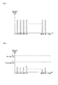
- Fig. 2 is an initial sequence-timing chart based on G. 992. 1.
- an ADSL modem of the transmitting side transmitting station
- an ADSL modem of the receiving side receiveiving station
- the REVERB signals are transmitted three times (C, R-REVERB1-3) between the transmitting and receiving stations in the initial sequence.
- the transmitting station after transmitting the third REVERB signal (C-REVERB3), the transmitting station transmits a SEGUE signal (C-SEGUE1), which indicates that data will follow.
- the transmitting station transmits C-RATES1 that sets the transmission speed, and C-MSG1 that sets additive information, such as a noise margin. Further, the transmitting station transmits C-MEDLEY that sets transmission speed and data bit numbers, which are attached to each carrier of multi carriers.
- the gain control apparatus 100 performs a gain control upon receiving the earlier REVERB signals (C-REVERB1, 2), especially the first REVERB signal (C-REVERB1). Accordingly, it is possible to perform a gain control even for REVERB signals appearing after the first REVERB signal (C-REVERB1), which is transmitted/received in the beginning.
- Fig. 3 illustrates frequency characteristics of the REVERB signals.
- lateral axis is frequency (f/kHz) and vertical axis is amount of energy (G/db).
- Fig. 3 illustrates frequency characteristics when REVERB signals are detected by a detector, such as a spectrum analyzer.
- each REVERB signal has frequency characteristics with signal energy of the same energy amount, in multiple carriers that are arranged from 1,1104 kHz to 4.3125 kHz period.
- the carriers are arranged at 4.3125 kHz periods; therefore, the REVERB signals have frequency characteristics that resemble teeth of a comb, as shown in the Fig. 3.
- the REVERB signals are only comprised of signal energy, and are not attached by data.
- the REVERB signals are designed to have such frequency characteristics as shown in Fig. 3, however, in real communication, the energy amounts of the signal energy that is attached to each carrier (carrier energy amounts) could decrease because of line conditions.
- Fig. 4 illustrates an example of frequency characteristics of REVERB signals when each carrier energy amount decreases.
- the carrier energy amount of 17.25 kHz shows the maximum amount, however, this energy amount is also much lower than the target minimum energy amount (second target level), which is described later.
- the gain control apparatus 100 uses the frequency characteristics of the REVERB signals, and performs appropriate gain controls in multi-carrier communication.
- the gain control apparatus 100 searches for the maximum carrier energy amount, among energy amounts of multiple carriers comprising REVERB signals, performs a gain control to bring the energy amount to the target energy level, and further performs the same gain control of the maximum carrier energy amount, for other carrier energy amounts across the board. Therefore, it is possible to perform a gain control without overflows, even in multi-carrier communication.
- Fig. 5 is a flowchart illustrating a gain control by the gain control apparatus 100.
- the gain control apparatus 100 always monitors the REVERB signal reception, when it is idle .
- Fig. 5 shows a flow after confirming the REVERB signal reception, in such a monitoring operation.
- the REVERB signal reception is confirmed upon detecting an FFT output for receiving a REVERB signal that has the above-described frequency characteristics. That is, the REVERB signal reception is confirmed upon detecting a signal that has the frequency characteristics as shown in Fig. 3.
- the gain control apparatus 100 Upon confirming the reception of a REVERB signal (ST 501), the gain control apparatus 100 waits for a symbol interruption when receiving a REVERB signal (ST 502). When confirming the reception of a REVERB signal, at the gain control apparatus 100, the process of the flow shown in Fig. 5 is repeated.
- a symbol interruption is performed approximately every 250. second.
- Sampling data of input signals is obtained approximately every 1. second.
- an A/D conversion process is performed at the A/D (D/A) converter 102, and data is output to the FFT processor 103.
- an FFT process is performed for this sampling data at the FFT processor 103 (ST 503). Specifically, when sampling data is accumulated for one symbol, an FFT process is performed each time.
- each sampling data is shown as a coordinate plot on a surface of R-I (Real-Imaginary). Then the coordinate information (R, I) according to each sampling data is stored in the buffer 106. In other words, for each FFT process, the coordinate information (R, I) associated with 250 sampling data is stored.
- Fig. 6 (a) is an image when coordinate information (R, I) according to 250 sampling data is stored in the buffer 106.
- the maximum amount searcher 107 searches for the maximum carrier energy amount, among energy amounts of multiple carriers that are comprising the REVERB signals, based on the coordinate information (R, I) (ST 504).
- the distance of the (R, I) coordinate plot of each sampling data, shown in the R-I surface, from the origin point, amounts to the energy amount of each carrier. Therefore, the maximum amount searcher 107 searches for the maximum carrier energy amount by comparing the distances of the (R, I) coordinate plot of each sampling data from the origin point.
- maximum carrier energy amount is searched for, by comparing the sum of the squares of each R and I value, on the coordinate plots of each sampling data, which is stored in the 106.
- Fig. 6 (b) is an image for a process to search for a maximum carrier amount according to the (R, I) coordination of each sampling data, performed by the maximum amount searcher 107. Using the example of Fig. 4, 17.25 kHz is found as a maximum carrier energy amount.
- the integration filer 108 performs a predetermined integral calculation for the maximum carrier energy amount, which is found by the maximum amount searcher maximum value searcher 107 (ST 505).
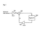
- Fig. 7 is a block diagram illustrating a configuration of the integration filter 108.
- the integration filer 108 outputs value A, to an adder 702, after the maximum carrier energy amount found by the maximum amount searcher 107 is multiplied by 0.1 in a multiplier 701 (ST 505). Also, the integration filer 108 outputs value B' to the adder 702, after value B stored in an inner register 703 is multiplied by 0.9 in a multiplier 704 (ST 506). Further, the integration filer 108 outputs, to the inner register 703, a sum B (summed by the adder 702) of value A (the input from the multiplier 701); and value B' (the input from the multiplier 704) (ST 507). This value B is stored in the inner register 703.
- the main controller 104 compares value B that is obtained from the integral calculation with the target maximum energy amount (the first target level) and the second target level.
- the main controller 104 checks whether value B is greater than the first target amount (ST 508). If value B is greater than the first target amount, the main controller 104 controls to decrease the carrier energy amount.
- the main controller 104 controls the gain controller 101 to decrease the energy amount of the input signal by 1db (ST 509). According to the control, the gain controller 101 decreases the energy amount of the input signal by 1db. Then the main controller 104 completes the gain control by the current symbol interruption.
- the gain controller 101 decreases all of the carrier energy amounts, which will be input later, by 1db across the board. Therefore, it is possible to control carrier energy amounts for all the input signals, based on the maximum carrier energy amount that is found by the maximum amount searcher 107.
- the main controller 104 checks whether value B is smaller than the second target level (ST 510). When value B is smaller than the second target level, the main controller 104 controls to increase the carrier energy amount.
- the main controller 104 controls the gain controller 101 to increase the energy amount of the input signal by 1db (ST 511). According to the control, the gain controller 101 increases the energy amount of the input signals by 1db. Then, the main controller 104 completes the gain control by the current symbol interruption.
- the gain controller 101 increases all of the carrier energy amounts across the board, which will be input later, by 1db. Therefore, it is possible to control carrier energy amounts for all the input signals, based on the maximum carrier energy amount that is found by the maximum amount searcher 107.
- Step 510 when value B is greater than the second target level, the main controller 104 determines that the gain control is not necessary, and terminates the process.
- Steps 508 - 511 The process of Steps 508 - 511 is explained in reference to Fig. 4.
- the energy amount for the first target level is "C” and the energy amount of the second target level is "D".
- a carrier energy amount of 17.25 kHz is found as the maximum carrier energy amount. The integral calculation is applied to this maximum amount, and value B is calculated.
- Step 508 checks whether the carrier energy amount, 17.25 kHz, is greater than "C", which is the first target level. As shown in the Fig. 4, the carrier energy amount, 17.25 kHz is smaller than the first target level "C"; therefore, Step 510 checks whether the energy amount is smaller than the second target level "D". As shown in Fig. 4, the carrier energy amount, 17.25 kHz is smaller than the second target level "D".
- the main controller 104 controls the gain controller 101 to increase the carrier energy amount of the input signal, by 1db. Under this control, the gain controller 101 increases all of the carrier energy amounts of the input signal by 1db across the board.
- the process of the flow is repeated to increase the energy amount, until the carrier energy amount, 17.25 kHz, becomes greater than the second target level "D".
- maximum carrier energy amount is searched for among the energy amounts of multiple carriers that comprise REVERB signals, and a gain control is performed to bring the energy amount to a target energy level.
- the same gain control for the maximum energy amount is performed for other carrier energy amounts across the board. Accordingly, it is possible to perform a gain control for signal degradation caused by line conditions and to prevent overflows of any other carriers at the same time. Therefore, it is possible to perform an appropriate gain control that prevents overflows in multi-carrier communication.
- Fig. 8 illustrates a situational example when an ADSL modem 800 that is provided with the gain control apparatus 100, is applied.
- the ADSL modem 800 that is provided with the gain control apparatus 100, is connected to, for example, a data communication apparatus 801, such as a PC, via a network, such as the Ethernet ®, at one end, and to the PSTN at the other end.
- a data communication apparatus 801 such as a PC
- a network such as the Ethernet ®
- the gain control apparatus 100 of the present invention performs a gain control for the signals that are input via the PSTN, as described above.
- the signals after the gain control process that is performed by the gain control apparatus 100 are stored in a memory 802.
- the communication processor 803 retrieves the signals after the gain control, which are stored in the memory 802, controls the communication with an ADSL modem at the other side, and performs a necessary communication process with the data communication apparatus 801 that is connected via the Ethernet ®.
- the communication processor 803 is able to perform the process in accordance with the signals after the gain control, which is stored in the memory 802. Therefore, it is possible to securely prevent communication errors due to the signal degradation caused by line conditions.
Landscapes
- Engineering & Computer Science (AREA)
- Computer Networks & Wireless Communication (AREA)
- Signal Processing (AREA)
- Telephonic Communication Services (AREA)
- Control Of Amplification And Gain Control (AREA)
Applications Claiming Priority (2)
| Application Number | Priority Date | Filing Date | Title |
|---|---|---|---|
| JP2001188227 | 2001-06-21 | ||
| JP2001188227A JP2003008536A (ja) | 2001-06-21 | 2001-06-21 | ゲインコントロール装置及びそれを備えたモデム装置 |
Publications (3)
| Publication Number | Publication Date |
|---|---|
| EP1278328A2 true EP1278328A2 (fr) | 2003-01-22 |
| EP1278328A3 EP1278328A3 (fr) | 2003-08-27 |
| EP1278328B1 EP1278328B1 (fr) | 2004-12-08 |
Family
ID=19027369
Family Applications (1)
| Application Number | Title | Priority Date | Filing Date |
|---|---|---|---|
| EP02010768A Expired - Lifetime EP1278328B1 (fr) | 2001-06-21 | 2002-05-14 | Modem avec dispositif de commande de gain |
Country Status (4)
| Country | Link |
|---|---|
| US (1) | US20020196874A1 (fr) |
| EP (1) | EP1278328B1 (fr) |
| JP (1) | JP2003008536A (fr) |
| DE (1) | DE60202177T2 (fr) |
Families Citing this family (2)
| Publication number | Priority date | Publication date | Assignee | Title |
|---|---|---|---|---|
| JP2004007269A (ja) | 2002-05-31 | 2004-01-08 | Panasonic Communications Co Ltd | Dslモデム装置及びdsl通信におけるイニシャライズ方法 |
| JP2005057449A (ja) * | 2003-08-01 | 2005-03-03 | Matsushita Electric Ind Co Ltd | Adslモデム装置及びその通信方法 |
Family Cites Families (9)
| Publication number | Priority date | Publication date | Assignee | Title |
|---|---|---|---|---|
| JPH06244878A (ja) * | 1993-02-18 | 1994-09-02 | Fujitsu Ltd | 変復調装置 |
| US5570093A (en) * | 1995-02-10 | 1996-10-29 | Applied Concepts, Inc. | Police traffic radar using absolute signal strength information to improve target signal processing accuracy |
| US6044107A (en) * | 1996-05-09 | 2000-03-28 | Texas Instruments Incorporated | Method for interoperability of a T1E1.4 compliant ADSL modem and a simpler modem |
| US6219378B1 (en) * | 1997-09-17 | 2001-04-17 | Texas Instruments Incorporated | Digital subscriber line modem initialization |
| US6452987B1 (en) * | 1998-11-25 | 2002-09-17 | Lucent Technologies Inc. | Fast start-up in discrete multi-tone (DMT) based communications system |
| US6771695B1 (en) * | 1999-07-30 | 2004-08-03 | Agere Systems Inc. | Low-complexity DMT transceiver |
| JP4378804B2 (ja) * | 1999-09-10 | 2009-12-09 | ソニー株式会社 | 撮像装置 |
| SE516879C2 (sv) * | 1999-11-23 | 2002-03-19 | Ericsson Telefon Ab L M | Signalnivåjusteringsanordning |
| US7020218B2 (en) * | 2001-06-18 | 2006-03-28 | Arnesen David M | Sliding-window transform with integrated windowing |
-
2001
- 2001-06-21 JP JP2001188227A patent/JP2003008536A/ja active Pending
-
2002
- 2002-05-08 US US10/140,161 patent/US20020196874A1/en not_active Abandoned
- 2002-05-14 DE DE60202177T patent/DE60202177T2/de not_active Expired - Fee Related
- 2002-05-14 EP EP02010768A patent/EP1278328B1/fr not_active Expired - Lifetime
Also Published As
| Publication number | Publication date |
|---|---|
| DE60202177T2 (de) | 2005-04-14 |
| JP2003008536A (ja) | 2003-01-10 |
| EP1278328A3 (fr) | 2003-08-27 |
| DE60202177D1 (de) | 2005-01-13 |
| EP1278328B1 (fr) | 2004-12-08 |
| US20020196874A1 (en) | 2002-12-26 |
Similar Documents
| Publication | Publication Date | Title |
|---|---|---|
| US9130810B2 (en) | OFDM communications methods and apparatus | |
| US6252900B1 (en) | Forward compatible and expandable high speed communications system and method of operation | |
| US5715277A (en) | Apparatus and method for determining a symbol rate and a carrier frequency for data transmission and reception | |
| US8498368B1 (en) | Method and system for optimizing gain changes by identifying modulation type and rate | |
| US7327794B2 (en) | Method and apparatus for detecting a jammed channel in a block oriented digital communication system | |
| US20020041643A1 (en) | Systems and methods for a multi-carrier transceiver with radio frequency interference reduction | |
| EP1061653A2 (fr) | Ajustement d'un étage de commande de gain analogique en utilisant un algorithme probabilistique | |
| US6400759B1 (en) | Device driver for rate adaptable modem with forward compatible and expandable functionality | |
| US6721394B1 (en) | Method for reducing noise from an asymmetric digital subscriber line modem | |
| EP1278328A2 (fr) | Modem avec dispositif de commande de gain | |
| US6836519B1 (en) | Automatic digital scaling for digital communication systems | |
| JP2003528542A (ja) | データネットワークにおいて複数の信号フォーマットのための入力利得を調整するための装置および方法 | |
| EP1451992B1 (fr) | Elimination d'interférences dans des récepteurs multiporteuses | |
| KR20070081381A (ko) | 직교 주파수 분할 다중 접속 방식의 무선 통신 시스템에서자동 이득 제어 장치 및 방법 | |
| US7260142B2 (en) | Dynamic hybrid switching in a wireline modem | |
| KR100391565B1 (ko) | 수정된 싱크보간법을 이용한 레일리페이딩 보상방법 | |
| EP1367791A2 (fr) | Controle de gain pour modem multiporteuse | |
| US20020039398A1 (en) | Apparatus and method for dynamic bit allocation for line-connected multi-carrier systems | |
| WO2001082545A2 (fr) | Dispositif et procede d'echantillonnage de signal a multiples vitesses d'horloge | |
| US20030194068A1 (en) | Digital communication system using telephone line and initializing method thereof | |
| EP1367792A2 (fr) | Dispositif pour modem LDN et procédé de réception pour la communication LDN | |
| JP2002512760A (ja) | バンド適応型復調のための方法と装置 | |
| JP3251935B2 (ja) | データ・モデム・レシーバ | |
| EP1503568A2 (fr) | Dispositif et procédé de communication de modem ADSL | |
| JP3113867B2 (ja) | ファクシミリモデム装置及びファクシミリ装置 |
Legal Events
| Date | Code | Title | Description |
|---|---|---|---|
| PUAI | Public reference made under article 153(3) epc to a published international application that has entered the european phase |
Free format text: ORIGINAL CODE: 0009012 |
|
| AK | Designated contracting states |
Kind code of ref document: A2 Designated state(s): AT BE CH CY DE DK ES FI FR GB GR IE IT LI LU MC NL PT SE TR |
|
| AX | Request for extension of the european patent |
Free format text: AL;LT;LV;MK;RO;SI |
|
| PUAL | Search report despatched |
Free format text: ORIGINAL CODE: 0009013 |
|
| AK | Designated contracting states |
Designated state(s): AT BE CH CY DE DK ES FI FR GB GR IE IT LI LU MC NL PT SE TR |
|
| AX | Request for extension of the european patent |
Extension state: AL LT LV MK RO SI |
|
| 17P | Request for examination filed |
Effective date: 20030910 |
|
| RAP1 | Party data changed (applicant data changed or rights of an application transferred) |
Owner name: PANASONIC COMMUNICATIONS CO., LTD. |
|
| 17Q | First examination report despatched |
Effective date: 20031112 |
|
| AKX | Designation fees paid |
Designated state(s): DE FR GB |
|
| GRAP | Despatch of communication of intention to grant a patent |
Free format text: ORIGINAL CODE: EPIDOSNIGR1 |
|
| GRAS | Grant fee paid |
Free format text: ORIGINAL CODE: EPIDOSNIGR3 |
|
| GRAA | (expected) grant |
Free format text: ORIGINAL CODE: 0009210 |
|
| AK | Designated contracting states |
Kind code of ref document: B1 Designated state(s): DE FR GB |
|
| REG | Reference to a national code |
Ref country code: GB Ref legal event code: FG4D |
|
| REG | Reference to a national code |
Ref country code: IE Ref legal event code: FG4D |
|
| REF | Corresponds to: |
Ref document number: 60202177 Country of ref document: DE Date of ref document: 20050113 Kind code of ref document: P |
|
| ET | Fr: translation filed | ||
| PLBE | No opposition filed within time limit |
Free format text: ORIGINAL CODE: 0009261 |
|
| STAA | Information on the status of an ep patent application or granted ep patent |
Free format text: STATUS: NO OPPOSITION FILED WITHIN TIME LIMIT |
|
| 26N | No opposition filed |
Effective date: 20050909 |
|
| PGFP | Annual fee paid to national office [announced via postgrant information from national office to epo] |
Ref country code: DE Payment date: 20070510 Year of fee payment: 6 |
|
| PGFP | Annual fee paid to national office [announced via postgrant information from national office to epo] |
Ref country code: GB Payment date: 20070509 Year of fee payment: 6 |
|
| PGFP | Annual fee paid to national office [announced via postgrant information from national office to epo] |
Ref country code: FR Payment date: 20070510 Year of fee payment: 6 |
|
| GBPC | Gb: european patent ceased through non-payment of renewal fee |
Effective date: 20080514 |
|
| REG | Reference to a national code |
Ref country code: FR Ref legal event code: ST Effective date: 20090119 |
|
| PG25 | Lapsed in a contracting state [announced via postgrant information from national office to epo] |
Ref country code: DE Free format text: LAPSE BECAUSE OF NON-PAYMENT OF DUE FEES Effective date: 20081202 Ref country code: FR Free format text: LAPSE BECAUSE OF NON-PAYMENT OF DUE FEES Effective date: 20080602 |
|
| PG25 | Lapsed in a contracting state [announced via postgrant information from national office to epo] |
Ref country code: GB Free format text: LAPSE BECAUSE OF NON-PAYMENT OF DUE FEES Effective date: 20080514 |