EP1282228A2 - Circuit de filtrage numérique - Google Patents
Circuit de filtrage numérique Download PDFInfo
- Publication number
- EP1282228A2 EP1282228A2 EP02017383A EP02017383A EP1282228A2 EP 1282228 A2 EP1282228 A2 EP 1282228A2 EP 02017383 A EP02017383 A EP 02017383A EP 02017383 A EP02017383 A EP 02017383A EP 1282228 A2 EP1282228 A2 EP 1282228A2
- Authority
- EP
- European Patent Office
- Prior art keywords
- outputs
- signal
- input
- weighting
- bit signals
- Prior art date
- Legal status (The legal status is an assumption and is not a legal conclusion. Google has not performed a legal analysis and makes no representation as to the accuracy of the status listed.)
- Withdrawn
Links
Images
Classifications
-
- H—ELECTRICITY
- H03—ELECTRONIC CIRCUITRY
- H03H—IMPEDANCE NETWORKS, e.g. RESONANT CIRCUITS; RESONATORS
- H03H17/00—Networks using digital techniques
- H03H17/02—Frequency selective networks
- H03H17/0223—Computation saving measures; Accelerating measures
- H03H17/0225—Measures concerning the multipliers
- H03H17/0226—Measures concerning the multipliers comprising look-up tables
-
- H—ELECTRICITY
- H03—ELECTRONIC CIRCUITRY
- H03H—IMPEDANCE NETWORKS, e.g. RESONANT CIRCUITS; RESONATORS
- H03H17/00—Networks using digital techniques
- H03H17/02—Frequency selective networks
- H03H17/06—Non-recursive filters
- H03H17/0607—Non-recursive filters comprising a ROM addressed by the input data signals
Definitions
- the present invention relates to a ROM (Read Only Memory) table lookup digital filter circuit which uses a ROM table for a multilevel input signal.
- ROM Read Only Memory
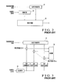
- Fig. 2 shows a digital filter circuit of the first prior art.
- a shift register 21 temporarily stores input 1-bit transmission data and outputs it to a ROM table 23.
- a counter 22 counts input sample clocks and outputs the obtained count value to the ROM table 23.
- the ROM table 23 outputs a filter output waveform, which is stored in advance and corresponds to the input data sequence, on the basis of the outputs from the shift register 21 and counter 22.
- This prior-art digital filter circuit is disclosed in Japanese Patent Laid-Open No. 63-69310.
- Fig. 3 shows a digital filter circuit of the second prior art.
- a shift register 31 serially receives transmission data of a plurality of bits and parallelly outputs the bit signals to multipliers 33-1 to 33-n.
- a counter 32 counts input sample clocks and outputs TAP coefficients corresponding to the count value to the multipliers 33-1 to 33-n.
- the multipliers 33-1 to 33-n weight the respective bit signals of the parallel outputs from the shift register 31 using the TAP coefficients and then outputs the bit signals to an adder 34.
- a digital filter circuit when the ROM table lookup filter shown in Fig. 2 is used, a digital filter circuit can easily be constituted. Generally, however, no ROM table lookup filter can be used for a multilevel signal containing a plurality of input bits. Hence, the normal FIR (inFinite Impulse Response) filter is normally used. However, since this circuit requires a number of multipliers, the circuit scale becomes large.
- FIR inFinite Impulse Response
- a digital filter circuit comprising decoding means for decomposing an input multilevel signal into a plurality of 1-bit signals, a plurality of ROM tables which output filter waveforms stored in advance, on the basis of the 1-bit signals output from the decoding means, and weighting and addition means for executing a plurality of weighting operations for respective bits of outputs from the ROM tables and then adding the outputs.
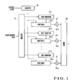
- Fig. 1 shows a digital filter circuit according to an embodiment of the present invention.
- a decoder 11 decomposes an input multilevel signal containing a plurality of bits into a plurality of 1-bit signals and outputs the 1-bit signals to shift registers 12-1, 12-2,..., 12-n.
- the shift registers 12-1, 12-2,..., 12-n serial/parallel-convert the 1-bit signals from the decoder 11 and output the 1-bit signals to ROM tables 13-1, 13-2,..., 13-n, respectively.
- a counter 15 counts sample clocks and outputs the count value to the ROM tables 13-1, 13-2,..., 13-n.
- the ROM tables 13-1, 13-2,..., 13-n output filter output waveforms, which are stored in advance and correspond to the input data sequence, to multipliers 14-1, 14-2,..., 14-n, respectively, on the basis of the outputs from the shift registers 12-1, 12-2,..., 12-n and the outputs from the counter 15.
- the adder 16 adds and outputs the outputs from the multipliers 14-1, 14-2,..., 14-n.
- a digital filter which receives a multilevel signal in which a ROM table lookup filter receives a multilevel signal containing a plurality of bits, will be described.
- the input multilevel signal is decomposed into a plurality of 1-bit signals by the decoder 11.
- the 1-bit signals are input to the ROM tables 13-1, 13-2,..., 13-n through the shift registers 12-1, 12-2,..., 12-n.
- ROM tables 13-1, 13-2,..., 13-n outputs that are preset and correspond to the input data sequences are read out on the basis of the outputs from the shift registers 12-1, 12-2,..., 12-n and the outputs from the counter 15.
- the respective bits of the outputs from the ROM tables 13-1, 13-2,..., 13-n are weighted by the multipliers 14-1, 14-2,..., 14-n and added by and output from the adder 16.
- the multilevel signal sequence containing a plurality of bits that construct input transmission data is decomposed by the decoder 11 into binary signal sequences formed from 1-bit signals of N sequence.
- R be the value of the input signal
- Dn be the nth signal obtained by the decomposition.
- the input signal sequence is so decomposed as to satisfy
- Outputs Fn from the ROM tables 13-1, 13-2,..., 13-n are weighted by the multipliers 14-1, 14-2,..., 14-in in accordance with equation (2) below and added by and output from the adder 16.
- G is the output from the adder 16.
- Dn ⁇ 1.
- a table used in a normal ROM lookup filter can be directly used as the data table of each ROM table.
- the input signal R may be expressed by offset binary data. Each bit of the binary signal may be decoded to obtain a signal sequence.
- a ROM table corresponding to an input value "+1" or "0" may be used.
- the input signal R is expressed by offset binary data, and each bit of the offset binary signal is used as a signal sequence obtained by decoding.
- the data table of the ROM table is different from that of a normal ROM lookup filter.
- a normal ROM lookup filter always processes an input value as "+1” or "-1".
- a table is prepared as convolution of an impulse response for an input signal sequence having a value "+1" or "-1". In the method of the present invention, however, since an input value is "+1" or "0", a corresponding table must be prepared.
- a ROM table can be used even for a multilevel input signal. For this reason, the circuit scale can be greatly reduced as compared to a conventional FIR filter.
Landscapes
- Engineering & Computer Science (AREA)
- Physics & Mathematics (AREA)
- Computer Hardware Design (AREA)
- Mathematical Physics (AREA)
- Computing Systems (AREA)
- Theoretical Computer Science (AREA)
- Filters That Use Time-Delay Elements (AREA)
- Cable Transmission Systems, Equalization Of Radio And Reduction Of Echo (AREA)
- Analogue/Digital Conversion (AREA)
- Compression, Expansion, Code Conversion, And Decoders (AREA)
Applications Claiming Priority (2)
| Application Number | Priority Date | Filing Date | Title |
|---|---|---|---|
| JP2001236697A JP2003046374A (ja) | 2001-08-03 | 2001-08-03 | デジタルフィルタ回路 |
| JP2001236697 | 2001-08-03 |
Publications (2)
| Publication Number | Publication Date |
|---|---|
| EP1282228A2 true EP1282228A2 (fr) | 2003-02-05 |
| EP1282228A3 EP1282228A3 (fr) | 2005-08-10 |
Family
ID=19067919
Family Applications (1)
| Application Number | Title | Priority Date | Filing Date |
|---|---|---|---|
| EP02017383A Withdrawn EP1282228A3 (fr) | 2001-08-03 | 2002-08-02 | Circuit de filtrage numérique |
Country Status (3)
| Country | Link |
|---|---|
| US (1) | US7068713B2 (fr) |
| EP (1) | EP1282228A3 (fr) |
| JP (1) | JP2003046374A (fr) |
Cited By (1)
| Publication number | Priority date | Publication date | Assignee | Title |
|---|---|---|---|---|
| RU2693595C1 (ru) * | 2018-03-15 | 2019-07-03 | Федеральное государственное бюджетное образовательное учреждение высшего образования "Юго-Западный государственный университет" (ЮЗГУ) | Способ фазовой привязки генерируемой последовательности импульсов к импульсу внешнего запуска |
Families Citing this family (5)
| Publication number | Priority date | Publication date | Assignee | Title |
|---|---|---|---|---|
| US7787520B2 (en) * | 2004-10-06 | 2010-08-31 | Broadcom Corporation | Method and system for channel estimation in a single channel (SC) single-input multiple-output (SIMO) system |
| US7873101B2 (en) * | 2005-03-25 | 2011-01-18 | Broadcom Corporation | Low latency digital filter and method |
| JP4217787B2 (ja) * | 2005-06-15 | 2009-02-04 | 国立大学法人東京工業大学 | 信号処理方法及び信号処理装置 |
| JP2007336474A (ja) * | 2006-06-19 | 2007-12-27 | Handotai Rikougaku Kenkyu Center:Kk | 信号処理方法及び信号処理装置 |
| US10019234B2 (en) | 2015-10-05 | 2018-07-10 | Altera Corporation | Methods and apparatus for sequencing multiply-accumulate operations |
Family Cites Families (13)
| Publication number | Priority date | Publication date | Assignee | Title |
|---|---|---|---|---|
| DE3579591D1 (de) * | 1984-11-22 | 1990-10-11 | Devon County Council | Daten-modulator-demodulatorsystem. |
| JPS61171215A (ja) | 1985-01-25 | 1986-08-01 | Nec Corp | 帯域制限フイルタ− |
| JPS62295506A (ja) | 1986-06-16 | 1987-12-22 | Toshiba Corp | デジタルフイルタ回路 |
| JPS6369310A (ja) | 1986-09-11 | 1988-03-29 | Nec Corp | デイジタルフイルタ |
| US4775851A (en) * | 1987-06-01 | 1988-10-04 | Motorola, Inc. | Multiplierless decimating low-pass filter for a noise-shaping A/D converter |
| JP2774501B2 (ja) * | 1987-11-05 | 1998-07-09 | 株式会社リコー | カラー画像の多値化階調処理方法 |
| JPH04100403A (ja) | 1990-08-20 | 1992-04-02 | Fujitsu Ltd | バイナリ・トランスバーサル・フイルタ |
| DE69024213T2 (de) * | 1990-09-18 | 1996-07-04 | Alcatel Nv | Mehrkanaliger Taktfrequenzreduzierer |
| JPH06104694A (ja) | 1992-09-22 | 1994-04-15 | Sony Corp | デジタルフィルタ |
| US5838725A (en) | 1996-12-06 | 1998-11-17 | U.S. Philips Corporation | Floating point digital transversal filter |
| WO2000062421A1 (fr) | 1999-04-14 | 2000-10-19 | Nokia Networks Oy | Filtre numerique et procede d'execution d'une multiplication sur la base d'une table de consultation |
| DE19919367A1 (de) | 1999-04-28 | 2000-12-07 | Siemens Ag | Verfahren und Vorrichtung zum Übertragen von Codemultiplexsignalen |
| EP1113580B1 (fr) | 1999-12-28 | 2015-02-25 | Hitachi Kokusai Electric Inc. | Codeur avec correction d'erreur, décodeur avec correction d'erreur ainsi qu'un appareil de transmission de données faisant usage du codeur et du décodeur |
-
2001
- 2001-08-03 JP JP2001236697A patent/JP2003046374A/ja active Pending
-
2002
- 2002-07-29 US US10/206,673 patent/US7068713B2/en not_active Expired - Fee Related
- 2002-08-02 EP EP02017383A patent/EP1282228A3/fr not_active Withdrawn
Cited By (1)
| Publication number | Priority date | Publication date | Assignee | Title |
|---|---|---|---|---|
| RU2693595C1 (ru) * | 2018-03-15 | 2019-07-03 | Федеральное государственное бюджетное образовательное учреждение высшего образования "Юго-Западный государственный университет" (ЮЗГУ) | Способ фазовой привязки генерируемой последовательности импульсов к импульсу внешнего запуска |
Also Published As
| Publication number | Publication date |
|---|---|
| JP2003046374A (ja) | 2003-02-14 |
| US20030033337A1 (en) | 2003-02-13 |
| US7068713B2 (en) | 2006-06-27 |
| EP1282228A3 (fr) | 2005-08-10 |
Similar Documents
| Publication | Publication Date | Title |
|---|---|---|
| US6243729B1 (en) | Digital finite-impulse-response (FIR) filter with a modified architecture based on high order Radix-N numbering | |
| JPH0435213A (ja) | フィルタ回路 | |
| GB2214386A (en) | Signal equaliser | |
| US5191547A (en) | Decimating digital finite impulse response filter | |
| EP1282228A2 (fr) | Circuit de filtrage numérique | |
| US8161092B2 (en) | Method and apparatus for efficient matrix multiplication in a direct sequence CDMA system | |
| US7945610B2 (en) | Convolution operation circuit | |
| EP1703637A2 (fr) | Filtre numérique à réponse impulsionnelle finie | |
| EP0990305B1 (fr) | Systeme de variation de la fourchette dynamique de coefficients dans un filtre numerique | |
| EP0464666B1 (fr) | Filtre transversal avec entrée pondérée | |
| US4800517A (en) | Word-sliced signal processor | |
| US7139341B2 (en) | Receiver circuit for a communications terminal and method for processing signals in a receiver circuit | |
| US7167514B2 (en) | Processing of quinary data | |
| KR100280497B1 (ko) | 격자구조의 이산 웨이브렛 변환 장치 | |
| US4931973A (en) | Method of generating updated transversal filter coefficients | |
| US6985522B2 (en) | Variable-gain digital filter | |
| US5956262A (en) | Digital filtering device | |
| EP0426296B1 (fr) | Appareil ayant une architecture d'interpolation modulaire | |
| KR100526074B1 (ko) | 5-레벨입력신호에응답하는등화기필터유닛에이용하는장치및방법 | |
| US5130942A (en) | Digital filter with front stage division | |
| KR100850703B1 (ko) | 샘플의 랭크를 결정하는 디바이스, 복수 샘플들의 랭크를결정하는 장치 및 i번째 랭크 오더 필터 | |
| US20020010727A1 (en) | Area efficient fir filter with programmable coefficients | |
| SU1661968A1 (ru) | Цифровой фильтр с многоуровневой дельта-модул цией | |
| EP1047221B1 (fr) | Générateur de code PN, dispositif de communication utilisant le générateur de code PN, système de communication et procédé de génération de code PN | |
| KR0155263B1 (ko) | 다차원 디지틀 필터 |
Legal Events
| Date | Code | Title | Description |
|---|---|---|---|
| PUAI | Public reference made under article 153(3) epc to a published international application that has entered the european phase |
Free format text: ORIGINAL CODE: 0009012 |
|
| AK | Designated contracting states |
Designated state(s): AT BE BG CH CY CZ DE DK EE ES FI FR GB GR IE IT LI LU MC NL PT SE SK TR |
|
| AX | Request for extension of the european patent |
Extension state: AL LT LV MK RO SI |
|
| PUAL | Search report despatched |
Free format text: ORIGINAL CODE: 0009013 |
|
| AK | Designated contracting states |
Kind code of ref document: A3 Designated state(s): AT BE BG CH CY CZ DE DK EE ES FI FR GB GR IE IT LI LU MC NL PT SE SK TR |
|
| AX | Request for extension of the european patent |
Extension state: AL LT LV MK RO SI |
|
| 17P | Request for examination filed |
Effective date: 20050722 |
|
| AKX | Designation fees paid |
Designated state(s): DE FR GB |
|
| STAA | Information on the status of an ep patent application or granted ep patent |
Free format text: STATUS: THE APPLICATION HAS BEEN WITHDRAWN |
|
| 18W | Application withdrawn |
Effective date: 20060412 |