EP1308761B1 - Ausrichtgerät für optische Fasern - Google Patents
Ausrichtgerät für optische Fasern Download PDFInfo
- Publication number
- EP1308761B1 EP1308761B1 EP01309227A EP01309227A EP1308761B1 EP 1308761 B1 EP1308761 B1 EP 1308761B1 EP 01309227 A EP01309227 A EP 01309227A EP 01309227 A EP01309227 A EP 01309227A EP 1308761 B1 EP1308761 B1 EP 1308761B1
- Authority
- EP
- European Patent Office
- Prior art keywords
- optical fibre
- fibre
- ball
- laser diode
- disk
- Prior art date
- Legal status (The legal status is an assumption and is not a legal conclusion. Google has not performed a legal analysis and makes no representation as to the accuracy of the status listed.)
- Expired - Lifetime
Links
- 239000013307 optical fiber Substances 0.000 title claims description 35
- 239000000835 fiber Substances 0.000 claims description 31
- 238000006073 displacement reaction Methods 0.000 claims description 22
- 230000008878 coupling Effects 0.000 claims description 21
- 238000010168 coupling process Methods 0.000 claims description 21
- 238000005859 coupling reaction Methods 0.000 claims description 21
- 239000000696 magnetic material Substances 0.000 claims description 2
- 239000000463 material Substances 0.000 description 13
- 238000000034 method Methods 0.000 description 12
- 239000010935 stainless steel Substances 0.000 description 6
- 229910001220 stainless steel Inorganic materials 0.000 description 6
- 230000003287 optical effect Effects 0.000 description 4
- 238000004519 manufacturing process Methods 0.000 description 3
- 230000035882 stress Effects 0.000 description 3
- 238000003466 welding Methods 0.000 description 3
- 229920000535 Tan II Polymers 0.000 description 2
- 230000032683 aging Effects 0.000 description 2
- SBYXRAKIOMOBFF-UHFFFAOYSA-N copper tungsten Chemical compound [Cu].[W] SBYXRAKIOMOBFF-UHFFFAOYSA-N 0.000 description 2
- 230000000694 effects Effects 0.000 description 2
- 229910000833 kovar Inorganic materials 0.000 description 2
- 229910052710 silicon Inorganic materials 0.000 description 2
- 239000010703 silicon Substances 0.000 description 2
- 230000008646 thermal stress Effects 0.000 description 2
- 229910001313 Cobalt-iron alloy Inorganic materials 0.000 description 1
- RYGMFSIKBFXOCR-UHFFFAOYSA-N Copper Chemical compound [Cu] RYGMFSIKBFXOCR-UHFFFAOYSA-N 0.000 description 1
- 229910052779 Neodymium Inorganic materials 0.000 description 1
- 229910001080 W alloy Inorganic materials 0.000 description 1
- KGWWEXORQXHJJQ-UHFFFAOYSA-N [Fe].[Co].[Ni] Chemical compound [Fe].[Co].[Ni] KGWWEXORQXHJJQ-UHFFFAOYSA-N 0.000 description 1
- 230000001154 acute effect Effects 0.000 description 1
- 239000000853 adhesive Substances 0.000 description 1
- 230000001070 adhesive effect Effects 0.000 description 1
- 230000000712 assembly Effects 0.000 description 1
- 238000000429 assembly Methods 0.000 description 1
- 230000009286 beneficial effect Effects 0.000 description 1
- 229910052802 copper Inorganic materials 0.000 description 1
- 239000010949 copper Substances 0.000 description 1
- 238000010438 heat treatment Methods 0.000 description 1
- 238000001746 injection moulding Methods 0.000 description 1
- 238000005304 joining Methods 0.000 description 1
- 230000007774 longterm Effects 0.000 description 1
- 229910052751 metal Inorganic materials 0.000 description 1
- 239000002184 metal Substances 0.000 description 1
- QEFYFXOXNSNQGX-UHFFFAOYSA-N neodymium atom Chemical compound [Nd] QEFYFXOXNSNQGX-UHFFFAOYSA-N 0.000 description 1
- 229910052761 rare earth metal Inorganic materials 0.000 description 1
- 150000002910 rare earth metals Chemical class 0.000 description 1
- 238000007789 sealing Methods 0.000 description 1
- 239000004065 semiconductor Substances 0.000 description 1
- 238000003892 spreading Methods 0.000 description 1
- WFKWXMTUELFFGS-UHFFFAOYSA-N tungsten Chemical compound [W] WFKWXMTUELFFGS-UHFFFAOYSA-N 0.000 description 1
- 229910052721 tungsten Inorganic materials 0.000 description 1
- 239000010937 tungsten Substances 0.000 description 1
Images



Classifications
-
- G—PHYSICS
- G02—OPTICS
- G02B—OPTICAL ELEMENTS, SYSTEMS OR APPARATUS
- G02B6/00—Light guides; Structural details of arrangements comprising light guides and other optical elements, e.g. couplings
- G02B6/24—Coupling light guides
- G02B6/42—Coupling light guides with opto-electronic elements
- G02B6/4201—Packages, e.g. shape, construction, internal or external details
- G02B6/4219—Mechanical fixtures for holding or positioning the elements relative to each other in the couplings; Alignment methods for the elements, e.g. measuring or observing methods especially used therefor
- G02B6/4236—Fixing or mounting methods of the aligned elements
- G02B6/4237—Welding
-
- G—PHYSICS
- G02—OPTICS
- G02B—OPTICAL ELEMENTS, SYSTEMS OR APPARATUS
- G02B6/00—Light guides; Structural details of arrangements comprising light guides and other optical elements, e.g. couplings
- G02B6/24—Coupling light guides
- G02B6/42—Coupling light guides with opto-electronic elements
- G02B6/4201—Packages, e.g. shape, construction, internal or external details
- G02B6/4219—Mechanical fixtures for holding or positioning the elements relative to each other in the couplings; Alignment methods for the elements, e.g. measuring or observing methods especially used therefor
- G02B6/422—Active alignment, i.e. moving the elements in response to the detected degree of coupling or position of the elements
- G02B6/4226—Positioning means for moving the elements into alignment, e.g. alignment screws, deformation of the mount
-
- G—PHYSICS
- G02—OPTICS
- G02B—OPTICAL ELEMENTS, SYSTEMS OR APPARATUS
- G02B6/00—Light guides; Structural details of arrangements comprising light guides and other optical elements, e.g. couplings
- G02B6/24—Coupling light guides
- G02B6/42—Coupling light guides with opto-electronic elements
- G02B6/4201—Packages, e.g. shape, construction, internal or external details
- G02B6/4219—Mechanical fixtures for holding or positioning the elements relative to each other in the couplings; Alignment methods for the elements, e.g. measuring or observing methods especially used therefor
- G02B6/422—Active alignment, i.e. moving the elements in response to the detected degree of coupling or position of the elements
- G02B6/4221—Active alignment, i.e. moving the elements in response to the detected degree of coupling or position of the elements involving a visual detection of the position of the elements, e.g. by using a microscope or a camera
- G02B6/4224—Active alignment, i.e. moving the elements in response to the detected degree of coupling or position of the elements involving a visual detection of the position of the elements, e.g. by using a microscope or a camera using visual alignment markings, e.g. index methods
Definitions
- This invention relates to a device for aligning an optical fibre with the output facet of a laser diode.
- Coupling efficiency between an optical fibre and a laser diode is limited by the accuracy and stability of the alignment achievable during the assembly process.
- Alignment of an optical fibre and a laser diode may be achieved by placing the optical fibre using a feature, which has been etched onto a silicon 'optical bench', upon which the laser diode has already been precisely attached.
- this simple technique is limited in precision by the manufactured accuracy of the silicon and the fibre and subsequent movement due to thermal stresses during the joining process.
- Another technique uses a mount to support the optical fibre. Once the laser and the optical fibre have been aligned and attached to the bench, the mount is mechanically deformed until an optimum coupling efficiency is achieved.
- JP-A-02245711 discloses an optical fibre aligned to a semiconductor chip with high accuracy.
- a ferrule is formed, which holds the fibre in such a manner that the front-end part of the ferrule forms a pivot bearing supporting the ferrule in a universal joint type together with the aperture of a supporting body.
- US Patent 6,074,103 discloses a method for aligning an optical fibre with an optical device mounted on a base by passing the fibre through two support members.
- US Patent 4,865,410 discloses a fibre optic feedthrough assembly, which uses a flexible material between the optical fibre and a mount.
- a high coupling efficiency between a fibre and a laser diode is aimed for, therefore it is important that the fibre tip is at an optimum distance from the laser diode, typically between 5 ⁇ m and 10 ⁇ m from the laser facet.
- the fibre tip is so close to the output facet of the laser this means that a small displacement from the optimum position causes a significant drop in coupling efficiency.
- displacements from the optimum position do not have such a great effect but coupling efficiency is reduced. Therefore it is important in a coupling device which is aiming for a high efficiency of coupling that the device is stable, i.e. that ageing does not cause the tip of the fibre to be displaced even a small amount from an optimum coupling position.
- This invention serves to alleviate such problems of reliability and stability, and is particularly beneficial for components requiring high reliability.
- a device for aligning an optical fibre with the output facet of a laser diode to obtain a substantially optimum coupling efficiency comprising the features of Claim 1.
- the universal joint may comprise a flexible material between the optical fibre and a mount.
- the adjustment means may comprise a disk supporting the optical fibre having a spring for biasing the ball into the socket, and in which displacement of the disk results in a pivotal movement of the fibre about the centre of the ball, and a corresponding smaller displacement of the end of the optical fibre.
- a laser diode 5 is mounted on a thermally conductive bench 3.
- the bench is fabricated from a material with a low thermal expansion coefficient such as Kovar, a nickel cobalt iron alloy.
- a material with a low thermal expansion coefficient such as Kovar, a nickel cobalt iron alloy.
- Other materials that work well include copper tungsten alloys which are materials which combine the conductivity of copper, thus providing heat spreading, with the low expansion coefficient of tungsten.
- Other suitable materials may be used for fabrication of the bench 3. It is possible to calculate limits for the thermal expansion of the chosen material, and to compensate for such expansion when designing the assembly.
- the bench 3 and an optical fibre 6, which is mounted in a stainless steel tube 8, are co-located in a mount 4.
- the optical fibre is inserted centrally in the stainless steel tube. Any misalignment of the optical fibre 6 with the centre of the tube 8 is compensated for during a passive alignment procedure, which is described later.
- the laser diode 5 is coupled directly to the fibre 6, without the necessity for a focussing lens between the end of the laser diode and the fibre core, although it will be understood by those skilled in the art that this invention is also applicable to alignment of a fibre with a laser diode where a focussing lens is used.
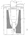
- the mount 4 has a hollow and generally cylindrical portion, which houses a ball 1.
- the ball 1 has an aperture passing through the centre, which receives the fibre 6 together with the tube 8.
- the ball 1 is biased against an internal conical socket in the mount, which has a co-axial aperture through which the optical fibre protrudes.
- the ball and the conical socket act together to form a universal joint with a pivotal point substantially at the centre of the ball 1.
- FIG 2 shows a sectional view from the side of the alignment device of figure 1, at the opposite end to the conical socket the generally cylindrical portion of the mount 4 has a larger aperture into which the fibre 6 together with the tube passes.
- the ball is fabricated from a magnetic material, which has been magnetised, the magnetic forces serving to bias the ball into the stainless steel conical socket.
- Rare earth magnets such as neodymium are especially suitable for this purpose as they have a high coercivity, which means that the magnetic forces will be greater for a lower volume of material.
- the laser diode 5 is aligned with the end of an optical fibre 6.
- Such alignment is referred to as passive alignment, because the devices are aligned optically (i.e. by eye with the aid of an optical microscope with approximately 50 to 250 times magnification).
- passive alignment lacks precision, firstly because although the laser diode generally has an active stripe which may be used to aid alignment, the position of the stripe may lack precision.
- the passive alignment procedure is a planar alignment, therefore, because the output facet of the laser may not be precisely manufactured such that the output facet may not be set at precisely 90° to the top and sides of the laser diode, the fibre 6 is unlikely to be in the optimum orientation after such passive alignment.
- the bench 3 After the fist stage of alignment the bench 3 is welded to the mount 4. During the welding process some relative movement between the laser diode 5 and the optical fibre 6 is likely to occur due to thermal stresses caused by the localised heating of material at the base of the bench 3.
- the light from the laser diode 5 is emitted in a conical shape. It is important to place the tip of the fibre at the point of maximum power.
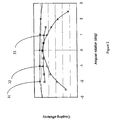
- Figure 3 illustrates an example of how coupling efficiency is affected by the angular orientation of the fibre in perpendicular planes, and also how the coupling efficiency is affected by coaxial rotation of the fibre.
- Rotation of the fibre in the vertical plane is illustrated by the line is illustrated by the line 32
- rotation in the horizontal plane is illustrated by the line 33
- coaxial rotation is illustrated by the line 31.
- Displacement of the disk 7 is used to finely align the end of the optical fibre 6 with the laser diode 5.
- This fine alignment is an active alignment, meaning that the alignment is carried out with the laser switched on, and the coupling between the laser diode 5 and the optical fibre 6, is measured. Once a maximum coupling efficiency is achieved then the laser diode and the optical fibre are considered to be optimally aligned.
- Displacement of the disk 7 causes rotation of the optical fibre 6 about the pivotal point of the universal joint formed by the ball and the conical socket.
- the ratio of the distance between the pivotal point and the disk, and the distance between the pivotal point and the end of the fibre is approximately 9:1 in this embodiment of the invention. Therefore, displacement of the disk by a particular amount, results in a corresponding displacement of the end of the fibre by one ninth that amount.
- the maximum rotation angle is set to 2°.
- Figure 4 illustrates an example lever design, where an optical fibre 42 pivots about a point 40.
- the fibre is rotated by displacement of the disk 7 and the power of the optical signal in the fibre is measured. Once the position at which a maximum power is obtained, that position is recorded as the optimum coupling position. Once the optimum coupling efficiency has been achieved during the active alignment procedure by displacement of the disk 7, the disk 7 is spot welded at three circumferentially equidistant points around the larger aperture of the mount 4. Three equidistant welded points have been found to be very stable, although it is possible to use more welds. In the welding machines used in the embodiment of the invention described, it is convenient to rotate the welder by 60° and spot weld at three more equidistant points to create six equidistant spot welds.
- any displacement of the disk will only cause a displacement of the fibre tip of one ninth of that displacement.
- the disk 7' is shown in more detail.
- the design of the disk 7' limits the amount of 'play' between the disk and the stainless steel tube 8' which occurs when the disk is displaced. If a circular aperture were used, for example, then the amount of play between the disk 7' and the tube 8' could be significant unless the aperture were precisely the same diameter as the tube 8'.
- the disk 7' is manufactured in such a way that the disk has built in concentric stresses, so that the disk has a high reluctance for coaxial misalignment.
- One technique is to use metal injection moulding to fabricate the disk. As the part shrinks built in stresses occur.
Landscapes
- Physics & Mathematics (AREA)
- General Physics & Mathematics (AREA)
- Optics & Photonics (AREA)
- Optical Couplings Of Light Guides (AREA)
Claims (3)
- Eine Vorrichtung zum Ausrichten einer optischen Faser (6) mit der Ausgangsfacette einer Laserdiode (5), um eine im Wesentlichen optimale Kopplungseffizienz zu erhalten, wobei die Vorrichtung folgende Merkmale aufweist:eine universelle Verbindung, durch die die optische Faser verläuft, derart, dass das Ende der optischen Faser benachbart zu der Ausgangsfacette der Laserdiode ist; undeine Einstellungseinrichtung (7), die bei einem Abstand von der universellen Verbindung positioniert ist, derart, dass eine Verschiebung der Einstellungseinrichtung eine Schwenkbewegung der Faser um einen Schwenkpunkt der universellen Verbindung bewirkt und in einer kleineren Verschiebung des Endes der optischen Faser resultiert, wobei die universelle Verbindung folgende Merkmale aufweist:eine Kugel (1), die eine Apertur durch die Mitte zum Aufnehmen der optischen Faser aufweist;eine Befestigung (4) zum Häusen der Kugel;eine Vorspanneinrichtung zum Vorspannen der Kugel in einen inneren konischen Sockel innerhalb der Befestigung, wobei der Sockel eine Apertur aufweist, durch die die optische Faser vorspringt, dadurch gekennzeichnet, dassdie Kugel magnetisiert ist und der konische Sockel ein magnetisches Material aufweist.
- Eine Vorrichtung gemäß dem vorhergehenden Anspruch, bei der die Einstellungseinrichtung eine Scheibe (7) aufweist, die die optische Faser trägt und eine Feder (9) zum Vorspannen der Kugel in den Sockel aufweist, und wobei eine Verschiebung der Scheibe in einer Schwenkbewegung der Faser um die Mitte der Kugel und einer entsprechenden kleineren Verschiebung des Endes der optischen Faser resultiert.
- Eine Vorrichtung gemäß einem der vorhergehenden Ansprüche, die ferner eine Fokussierlinse aufweist, die zwischen dem Ende der optischen Faser und der Ausgangsfacette der Laserdiode positioniert ist.
Priority Applications (3)
| Application Number | Priority Date | Filing Date | Title |
|---|---|---|---|
| EP01309227A EP1308761B1 (de) | 2001-10-31 | 2001-10-31 | Ausrichtgerät für optische Fasern |
| DE60109456T DE60109456T2 (de) | 2001-10-31 | 2001-10-31 | Ausrichtgerät für optische Fasern |
| US10/241,020 US6910811B2 (en) | 2001-10-31 | 2002-09-11 | Optical fiber alignment device and method |
Applications Claiming Priority (1)
| Application Number | Priority Date | Filing Date | Title |
|---|---|---|---|
| EP01309227A EP1308761B1 (de) | 2001-10-31 | 2001-10-31 | Ausrichtgerät für optische Fasern |
Publications (2)
| Publication Number | Publication Date |
|---|---|
| EP1308761A1 EP1308761A1 (de) | 2003-05-07 |
| EP1308761B1 true EP1308761B1 (de) | 2005-03-16 |
Family
ID=8182409
Family Applications (1)
| Application Number | Title | Priority Date | Filing Date |
|---|---|---|---|
| EP01309227A Expired - Lifetime EP1308761B1 (de) | 2001-10-31 | 2001-10-31 | Ausrichtgerät für optische Fasern |
Country Status (3)
| Country | Link |
|---|---|
| US (1) | US6910811B2 (de) |
| EP (1) | EP1308761B1 (de) |
| DE (1) | DE60109456T2 (de) |
Families Citing this family (6)
| Publication number | Priority date | Publication date | Assignee | Title |
|---|---|---|---|---|
| US20030095755A1 (en) * | 2001-11-16 | 2003-05-22 | Vladimir Vaganov | Feature and method to align and assemble photonic components |
| US20080013908A1 (en) * | 2006-01-03 | 2008-01-17 | 3M Innovative Properties Company | Total internal reflection prism mount |
| FR2962231B1 (fr) * | 2010-07-02 | 2014-10-31 | Alcatel Lucent | Procede d'alignement et de fixation d'une fibre optique couplee a un composant optoelectronique |
| US8632262B2 (en) * | 2011-08-30 | 2014-01-21 | Kestrel Labs, Inc. | Laser to fiber optical coupling in photoplethysmography |
| JP2015016073A (ja) * | 2013-07-10 | 2015-01-29 | ウシオ電機株式会社 | 光ファイバーユニット |
| HUP1800439A2 (hu) | 2018-12-20 | 2020-06-29 | Equip Test Kft | Csatlakozószerkezet optikai vezetékek csatlakoztatására, valamint krimpelõ eszköz és kinyomó eszköz ahhoz |
Family Cites Families (12)
| Publication number | Priority date | Publication date | Assignee | Title |
|---|---|---|---|---|
| JPS5949708B2 (ja) * | 1979-06-13 | 1984-12-04 | 三菱電機株式会社 | 光半導体装置 |
| JPS6043889A (ja) * | 1983-08-22 | 1985-03-08 | Hitachi Ltd | 光ファイバー付レーザーダイオード装置の組立方法 |
| US4865410A (en) * | 1988-01-25 | 1989-09-12 | E. I. Du Pont De Nemours And Company | Decoupled fiber optic feedthrough assembly |
| JPH02245711A (ja) * | 1989-03-20 | 1990-10-01 | Fujitsu Ltd | 光ファイバ固定装置 |
| IT1239223B (it) * | 1990-02-20 | 1993-09-28 | Pirelli Cavi Spa | Connettore ottico orientabile per collegamento di fibre ottiche a componenti ottici discreti e sensore impiegante uno o piu' connettori orientabili |
| JPH1096839A (ja) * | 1996-09-20 | 1998-04-14 | Sumitomo Electric Ind Ltd | 半導体レーザモジュールの製造方法 |
| US6074103A (en) * | 1996-10-15 | 2000-06-13 | Sdl, Inc. | Aligning an optical fiber with electroluminescent semiconductor diodes and other optical components |
| US5937123A (en) * | 1998-04-22 | 1999-08-10 | Eastman Kodak Company | Fiber optical laser collimating device |
| US6164837A (en) * | 1998-12-30 | 2000-12-26 | Mcdonnell Douglas Corporation | Integrated microelectromechanical alignment and locking apparatus and method for fiber optic module manufacturing |
| KR100322134B1 (ko) * | 1999-02-06 | 2002-03-18 | 윤종용 | 광원과 광섬유의 정렬 장치 및 이를 구비하는 광원 모듈 |
| US6652158B2 (en) * | 2000-09-05 | 2003-11-25 | Optical Zonu Corporation | Optical networking unit employing optimized optical packaging |
| US6709169B2 (en) * | 2000-09-28 | 2004-03-23 | Powernetix, Inc. | Thermally and mechanically stable low-cost high thermal conductivity structure for single-mode fiber coupling to laser diode |
-
2001
- 2001-10-31 DE DE60109456T patent/DE60109456T2/de not_active Expired - Lifetime
- 2001-10-31 EP EP01309227A patent/EP1308761B1/de not_active Expired - Lifetime
-
2002
- 2002-09-11 US US10/241,020 patent/US6910811B2/en not_active Expired - Lifetime
Also Published As
| Publication number | Publication date |
|---|---|
| US6910811B2 (en) | 2005-06-28 |
| DE60109456D1 (de) | 2005-04-21 |
| US20030081912A1 (en) | 2003-05-01 |
| EP1308761A1 (de) | 2003-05-07 |
| DE60109456T2 (de) | 2006-04-13 |
Similar Documents
| Publication | Publication Date | Title |
|---|---|---|
| KR920010947B1 (ko) | 광결합장치와 그 제조방법, 발광장치와 그 조립방법 및 렌즈홀더 | |
| US6709169B2 (en) | Thermally and mechanically stable low-cost high thermal conductivity structure for single-mode fiber coupling to laser diode | |
| KR0171374B1 (ko) | 광집속렌즈를 포함하는 레이저 모듈 및 그 렌즈 고정방법 | |
| JP2875812B2 (ja) | 光ファイバと半導体レーザダイオード間にカップリングを有するオプトエレクトロニク装置 | |
| US6757308B1 (en) | Hermetically sealed transmitter optical subassembly | |
| US6409398B2 (en) | Optical module and manufacturing method of optical module | |
| JP5411399B2 (ja) | 光電子アセンブリおよびその組立て方法 | |
| US6087621A (en) | Method for laser hammering a multi-channel optoelectronic device module | |
| JP3731754B2 (ja) | 構成要素に導波管を結合するための方法および装置 | |
| EP1308761B1 (de) | Ausrichtgerät für optische Fasern | |
| JP2002014257A (ja) | 半導体レーザモジュール | |
| CA2374500A1 (en) | Semiconductor laser module and method for optically coupling laser light and optical fiber | |
| US6492614B2 (en) | System and process for magnetic fixturing of optical components on bench for solder attach | |
| US6843609B2 (en) | Optical module with lens holding member | |
| JPH085876A (ja) | 光伝送用モジュール及びそれに用いられるレンズホルダ部材 | |
| EP1186923B1 (de) | Vorrichtung zur Ausrichtung optischer Quellen und optischer Fasern in einem optischen Quellen-Modul | |
| JPH07140361A (ja) | 光伝送用モジュール及びそれに用いられるレンズホルダー受け | |
| US6603093B2 (en) | Method for alignment of optical components using laser welding | |
| JPH07168065A (ja) | 光半導体モジュール | |
| JP3429190B2 (ja) | 光半導体装置 | |
| JPH02308209A (ja) | 半導体発光装置及びその部品並びにレンズ位置調整方法 | |
| JP2005070568A (ja) | 光モジュール | |
| JPH03100506A (ja) | 光結合装置及び光部品 | |
| US20040264870A1 (en) | Optical alignment mount with height adjustment | |
| JPH0943455A (ja) | 光モジュール |
Legal Events
| Date | Code | Title | Description |
|---|---|---|---|
| PUAI | Public reference made under article 153(3) epc to a published international application that has entered the european phase |
Free format text: ORIGINAL CODE: 0009012 |
|
| AK | Designated contracting states |
Designated state(s): AT BE CH CY DE DK ES FI FR GB GR IE IT LI LU MC NL PT SE TR |
|
| AX | Request for extension of the european patent |
Extension state: AL LT LV MK RO SI |
|
| 17P | Request for examination filed |
Effective date: 20031107 |
|
| AKX | Designation fees paid |
Designated state(s): DE FR GB |
|
| 17Q | First examination report despatched |
Effective date: 20040119 |
|
| GRAP | Despatch of communication of intention to grant a patent |
Free format text: ORIGINAL CODE: EPIDOSNIGR1 |
|
| RTI1 | Title (correction) |
Free format text: OPTICAL FIBRE ALIGNMENT DEVICE |
|
| GRAS | Grant fee paid |
Free format text: ORIGINAL CODE: EPIDOSNIGR3 |
|
| GRAA | (expected) grant |
Free format text: ORIGINAL CODE: 0009210 |
|
| AK | Designated contracting states |
Kind code of ref document: B1 Designated state(s): DE FR GB |
|
| REG | Reference to a national code |
Ref country code: GB Ref legal event code: FG4D |
|
| REF | Corresponds to: |
Ref document number: 60109456 Country of ref document: DE Date of ref document: 20050421 Kind code of ref document: P |
|
| PGFP | Annual fee paid to national office [announced via postgrant information from national office to epo] |
Ref country code: FR Payment date: 20051017 Year of fee payment: 5 |
|
| PLBE | No opposition filed within time limit |
Free format text: ORIGINAL CODE: 0009261 |
|
| STAA | Information on the status of an ep patent application or granted ep patent |
Free format text: STATUS: NO OPPOSITION FILED WITHIN TIME LIMIT |
|
| ET | Fr: translation filed | ||
| 26N | No opposition filed |
Effective date: 20051219 |
|
| REG | Reference to a national code |
Ref country code: GB Ref legal event code: 732E |
|
| PGFP | Annual fee paid to national office [announced via postgrant information from national office to epo] |
Ref country code: GB Payment date: 20061025 Year of fee payment: 6 |
|
| REG | Reference to a national code |
Ref country code: FR Ref legal event code: ST Effective date: 20070629 |
|
| PG25 | Lapsed in a contracting state [announced via postgrant information from national office to epo] |
Ref country code: FR Free format text: LAPSE BECAUSE OF NON-PAYMENT OF DUE FEES Effective date: 20061031 |
|
| GBPC | Gb: european patent ceased through non-payment of renewal fee |
Effective date: 20071031 |
|
| PG25 | Lapsed in a contracting state [announced via postgrant information from national office to epo] |
Ref country code: GB Free format text: LAPSE BECAUSE OF NON-PAYMENT OF DUE FEES Effective date: 20071031 |
|
| PGFP | Annual fee paid to national office [announced via postgrant information from national office to epo] |
Ref country code: DE Payment date: 20101027 Year of fee payment: 10 |
|
| PG25 | Lapsed in a contracting state [announced via postgrant information from national office to epo] |
Ref country code: DE Free format text: LAPSE BECAUSE OF NON-PAYMENT OF DUE FEES Effective date: 20120501 |
|
| REG | Reference to a national code |
Ref country code: DE Ref legal event code: R119 Ref document number: 60109456 Country of ref document: DE Effective date: 20120501 |