EP1308997A2 - Dispositif semi-conducteur pour detecter des charges, système se composant d'un dispositif semi-conducteur pour détecter des charges, un dispositif semi-conducteur de référence, tranche, utlisation d'une tranche et méthode pour mesurer qualitativement le charge d'une tranche - Google Patents
Dispositif semi-conducteur pour detecter des charges, système se composant d'un dispositif semi-conducteur pour détecter des charges, un dispositif semi-conducteur de référence, tranche, utlisation d'une tranche et méthode pour mesurer qualitativement le charge d'une tranche Download PDFInfo
- Publication number
- EP1308997A2 EP1308997A2 EP02102534A EP02102534A EP1308997A2 EP 1308997 A2 EP1308997 A2 EP 1308997A2 EP 02102534 A EP02102534 A EP 02102534A EP 02102534 A EP02102534 A EP 02102534A EP 1308997 A2 EP1308997 A2 EP 1308997A2
- Authority
- EP
- European Patent Office
- Prior art keywords
- gate
- capacitance
- wafer
- semiconductor component
- detector
- Prior art date
- Legal status (The legal status is an assumption and is not a legal conclusion. Google has not performed a legal analysis and makes no representation as to the accuracy of the status listed.)
- Withdrawn
Links
Images


Classifications
-
- H—ELECTRICITY
- H10—SEMICONDUCTOR DEVICES; ELECTRIC SOLID-STATE DEVICES NOT OTHERWISE PROVIDED FOR
- H10P—GENERIC PROCESSES OR APPARATUS FOR THE MANUFACTURE OR TREATMENT OF DEVICES COVERED BY CLASS H10
- H10P74/00—Testing or measuring during manufacture or treatment of wafers, substrates or devices
- H10P74/27—Structural arrangements therefor
- H10P74/277—Circuits for electrically characterising or monitoring manufacturing processes, e.g. circuits in tested chips or circuits in testing wafers
Definitions
- the invention relates to a charge detector semiconductor component in the form of a a semiconductor material applied structure that is a non-volatile memory cell has, in the form of a MOS field effect transistor with a transistor gate and one MOS capacitance with a capacitance gate.
- the invention further relates to System of a charge detector semiconductor device and a reference semiconductor device.
- the invention further relates to a wafer and the use of a Wafers with a number of charge detector semiconductor devices and / or systems.
- the invention relates to a method for qualitative and quantitative Measurement of a charge on a wafer during the processing of the wafer.
- Wafer charging, wafer "charging”, is a phenomenon that occurs during manufacture of semiconductor components occurs continuously because many process steps in the Plasma take place or be carried out with charged particles. especially the thin gate oxides of MOS transistors in CMOS-like technologies, i.e. CMOSund BICMOS or similar technologies can be used during a process step on conductive surfaces, e.g. Polysilicon or metal, collected cargo and the resulting tunnel current can be destroyed. This charging is often a cause for a low production yield.
- the process control using a CHARM wafer is complex and expensive, especially since a production for measuring one or more CHARM wafers must be stopped.
- JP-10-284726 describes one of a p-channel and an n-channel MOS transistor existing structure and a method for measuring wafer charging in plasma containing Environment described.
- the structure requires measurement before and after the plasma process step. This is only possible if the structure is contacted. Thus, the Control of production goods with the structure at most for plasma steps at the end of the Manufacturing process are used.
- test wafers e.g. known as a CHARM wafer for which Control needed.
- JP-10-284726 and US 5,959,309 enable also no very precise assessment of the charging. In particular, there is no analysis for any process step possible.
- the structures are not compatible with the CMOS manufacturing processes, since it has no CMOS technology-like structure and no CMOS technology-like structure Have interconnection, so that a number of CMOS technology standards go beyond Process steps are necessary.
- the structure of JP 10-284726 is not compatible with the standard CMOS manufacturing process since it is two Polysilicon levels (4 and 3 in Figure 3) used.
- the structure in the US patent 5,959,309 is not compatible with the standard CMOS manufacturing process as it on the one hand uses a high quality capacity (46 in FIGS. 4a and 4b) which usually in a CMOS process with two superimposed polysilicon levels would manufacture. As a result, compared to the standard CMOS process an additional level of polysilicon is also required.
- the photodiode string requires (43 in FIG. 4a) that the layers lying above the photodiode are transparent are.
- this does not have to be the case in a standard CMOS process.
- a silicon semiconductor may not be able to completely emit plasma radiation Absorb spectrum range.
- the object of the present invention is to provide a structure based on a non-volatile Storage structure based and as a Process Control Monitor (PCM) structure acts. It is also the task of specifying a use of the structure and a method with which the charge can be measured, which during a process step on a Wafers have been created in a specific location, the structure during production and / or processing of the wafer in a CMOS or BICMOS technology is.
- PCM Process Control Monitor
- the invention achieves the object with regard to the structure according to a first variant of a charge detector semiconductor component in the form of a structure applied to a semiconductor material, which has a non-volatile memory cell, in the form a MOS field effect transistor with a transistor gate, advantageously also source and drain, and a MOS capacitance with a capacitance gate, advantageously also source and drain.
- a charge detector semiconductor component in the form of a structure applied to a semiconductor material, which has a non-volatile memory cell, in the form a MOS field effect transistor with a transistor gate, advantageously also source and drain, and a MOS capacitance with a capacitance gate, advantageously also source and drain.
- the invention provides: An antenna that is operatively connected to the capacitance gate, wherein the capacitance gate is connected to the transistor gate by means of a further operative connection in such a way that charging of the antenna can be stored via the memory cell and can be called up when required, and the structure has a structure that resemble
- a system comprising a charge detector semiconductor component and a reference semiconductor component, in the form of a structure applied to a semiconductor material, the charge detector semiconductor component being a non-volatile detector Memory cell in shape a first MOS field effect transistor with a detector transistor gate, advantageously also source and drain, and a first MOS capacitance with a detector capacitance gate, advantageously also source and drain, and comprising an antenna connected to the detector capacitance gate by a first operative connection, wherein the detector capacitance gate is connected by means of a first operative connection, the detector capacitance gate being connected to the detector transistor gate by means of a further first operative connection, and wherein the reference semiconductor component has a non-volatile reference memory cell, in the form of a second MOS field-effect transistor with a reference transistor gate, advantageously also source and drain, and a second MOS capacitance with a reference capacitance Gate, advantageously also source and drain, and
- the invention is based on the knowledge that it is possible to use the structure in the first and second variant used in the production of the wafer in each To produce CMOS / BICMOS standard processes. So the structure has a CMOS technology-like Building on. That is, only units are used in the structure made that also used in every standard CMOS / BICMOS process are to be produced. In particular, devices such as NMOS and PMOS transistors Made use of. Such units are available in every CMOS process. The above structure can thus be present on every production wafer without additional ones Process steps would be necessary.
- PCM structure Process Control Monitor structure
- the above PCM structure is able to charge what non-volatile storage occurs during process control.
- the used PCM structure above a non-volatile memory cell usually require additional process steps so that the use in a standard CMOS or BICMOS technology or similar technologies so far not possible. Additional process steps or a change in the process sequence for production
- the structure in a standard CMOS process is in the above PCM structure however, not necessary after the knowledge of the invention.
- the structure is therefore on the one hand cost-neutral to manufacture and offers on the other hand, the only way to get production goods when processing the wafer monitor without delaying the production process.
- the production goods Cost-effectively continuously monitored and a continuous assessment of the charging to be hit.
- expensive test wafers are avoided.
- a charge detector semiconductor component and / or a reference semiconductor component preferably has a first area with the MOS field effect transistor and one first well and a second area with the MOS capacitance and a second well, on, the first well and the second well having different signs are.
- the first trough is a p-trough and the second trough is an n-trough.
- the MOS field effect transistor is an NMOS field effect transistor
- the MOS capacitance is a layered polysilicon / n-well capacitance.
- the antenna, the capacitance gate and the Transistor gate conductively connected, in particular galvanically connected.
- a control gate through a trough or the source / drain connections is advantageous Capacity formed. This has the additional advantage that the memory cell is special can be read out cheaply.
- the transistor gate and the capacitance gate are advantageous as a polysilicon plate executed.
- the structure of the first and the second variant is constructed such that the Semiconductor material is arranged in a first level on which the non-volatile memory cell is brought up in a second level, on which in turn the connections, the Transistor gate, the capacitance gate and the antenna or the ground line in one third level is applied. It turns out to be particularly favorable that the transistor gate and the capacitance gate are connected together in a polysilicon level.
- a structure according to one of these developments has the advantage that a manufacturing process for the structure compatible with the CMOS-like manufacturing processes, especially the standard CMOS method.
- the antenna can advantageously be compatible to run on standard CMOS technology.
- the antenna can be used as one Polysilicon layer can be executed.
- the antenna is advantageously designed with a single polysilicon layer.
- you can the antenna can also be made of metal.
- the antenna can also be used as a Contact antenna, in particular via antenna.
- the antenna is advantageous as a MOS capacitance, in particular as an NMOS capacitance, executed. This ensures that all levels in which charging occurs can be controlled.
- the invention further extends to a wafer in which the aforementioned features of the Developments of the invention can be implemented.
- the invention provides a solution the task regarding the wafer, a wafer, for example a silicon wafer, the according to the invention with a number of charge detector semiconductor components of the above type and / or systems of the type mentioned above is designed.
- a production wafer i.e. not a test wafer on which the above mentioned structure is processed together with the production goods.
- the structure can also be produced on the production wafer. In both In some cases, the production or processing takes place in a CMOS-antigen technology. This has the advantage that the structure is present on every production wafer.
- the above structure is housed in a saw line of the wafer, which is advantageous effectively uses the available space on the wafer.
- the processing of the Production goods take place on the remaining area of the wafer.
- the above structure according to a predetermined location Distribution on the wafer produced and / or processed. This enables a spatially resolved and / or process-selective measurement of a charge.
- one use is to solve the problem with regard to use a wafer of the above type with a number of charge detector semiconductor devices of the above type and / or systems of the above type for qualitative and quantitative measurement of a charge, in particular plasma-induced charge of the wafer during the processing of the wafer.
- the invention is a predetermined local distribution of the number of spatially resolved and / or process step-selective measurement of a charge, in particular plasma-induced Charging, the wafer is provided in the processing of the wafer.
- the wafer with a number of predetermined, locally distributed systems is advantageous manufactured.
- the threshold voltage of the Charge detector semiconductor device with the threshold voltage of the reference semiconductor device compared.
- the drain currents can also be used with control gate potentials applied in the same way in each case compared to the charge detector component and the reference semiconductor component become.
- the control gate potential is in particular through a tub or Source / drain connections of the capacitance of the detector semiconductor component and the Reference semiconductor device formed.
- the non-volatile memory cell of an NMOS transistor and a layered polysilicon / n-well capacitance there is the non-volatile memory cell of an NMOS transistor and a layered polysilicon / n-well capacitance.
- the n + diffusion areas of the poly / n well capacity can be arbitrarily through p + diffusion areas be replaced.
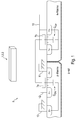
- the gate of the NMOS transistor 7a and a polysilicon plate layered poly / n-well capacitance 7b are common in a polysilicon level galvanically connected.
- the antenna 1, 2 or 3 is galvanically connected to the polysilicon plate connected, which is part of the capacitance gate 7b.
- This unit has the Function of a floating gate 7.
- the control gate 10 is through the n-well of the capacitance or the n + connections the layered polysilicon / n-well capacitance.
- the drain connector 12 of the NMOS transistor provides the read connection of the wafer charging detector Device represents. 11 denotes the source, 12 the drain and 13 the p-sub connection of the p-well of the NMOS transistor.
- the source connection 12 forms the write connection 12 (Bit line).
- the antenna 1, 2, 3 is electrically connected to the capacitance gate 7.
- the Gatt capacitance C GP and C GN are also indicated schematically by symbols.
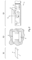
- the possible antennas are shown in detail in FIG. 2.
- the antenna is (a) Polysilicon or metal plate, (b) a contact or via and (c) a MOS capacitance possible.
- an antenna can be designed as a polysilicon or metal plate. It can e.g. as an interconnect antenna with a first metallization level (IN) and a second metallization level (INS), ie as an IN or INS antenna.
- INS second metallization level
- antenna 2 can be a contact or a via or more Contacts or vias, e.g. as a contact (CO) or another contact (COS) structure with a cover layer made of a polysilicon (PS), an icing metallization (IN) or a second metallization (INS) structure.
- CO contact
- COS contact
- PS polysilicon
- I icing metallization
- INS second metallization
- an antenna 3 can be used as a MOS structure, e.g. as a MOS capacitance, an NMOS transistor, PMOS transistor, as a bipolar implant antenna or as another polysilicon (PSS) structure can be formed.
- PSS polysilicon
- the MOS capacitance is an antenna for implants.
- an implanter antenna is also given by the polysilicon plate when it is implanted.
- C GN is the NMOST gate capacitance. In all three cases, 4 is connected to the floating gate. In Figure 2 (c) 5 is connected to the control gate. 6 denotes an n-well.
- FIG. 3 shows the complete wafer charging detector device 9 with the contact of the different antennas 1, 2 and 3 according to FIG. 2.
- antenna 1 or 2 over 4 with the floating gate 7 of the polysilicon / n-well capacitance connected.
- the antenna is designed as a PMOS transistor.
- the gate of the antenna 3 is via 4 with the floating gate 7 of the polysilicon / n-well capacitance connected and the control gate of the antenna via 5 to the control gate 10 of the polysilicon / n-well capacity.
- Wafer Charging Detector Device The function of the Wafer Charging Detector Device is described below.
- a positive read voltage is applied to control gate 10.
- the substrate connection 13 is at ground potential.
- the read voltage drops approximately at the series capacitors C GP and C GN .
- the capacitance gate potential V FG is dependent on the ratio of the gate capacitances C GP , C GN , the capacitance of the antenna 1, 2 or 3 (C antenna ) and the charge Q antenna on the antenna 1, 2 or 3 or the capacity gate.
- V FG ⁇ V reference FG + 1 C Antenna ges Q Antenna
- the potential coupled to the capacitance gate is greater than the threshold voltage of the NMOS transistor, is formed under the gate between source and drain diffusions of the NMOS transistor from an inversion layer.
- the NMOS transistor of the wafer Charging Detector Device is therefore switched on. When the drain voltage is applied, a Current flow at the drain can be detected.
- antenna 1, 2 or 3 is negatively charged during production, the negative charge to an accumulation of positive charge carriers between the source / drain diffusions of the wafer charging detector device. The same applied reading voltage is then no longer sufficient to form an inversion layer. As a result, the NMOS transistor. There is no current flow at the drain connection when the drain voltage is applied be determined.
- antenna 1, 2 or 3 is positively charged during production, the positive charge to an inversion layer between the source / drain diffusions of the wafer Charging detector device.
- the NMOS transistor is without a read voltage switched on. A current flow can occur at the drain connection when the drain voltage is applied be determined.
- the detected current of the Wafer Charging Detector Device 9 can be described for all cases by the following expression:
- the evaluation of the wafer is Charging Detector Devices 9 described below.
- the charge generated during a process step on the wafer charging detector Device 9 can be compared during the process control monitor (PCM) measurement with a reference structure 19 according to FIG. 5 of the wafer charging detector device according to Figure 1 are evaluated.
- the reference structure which is basically the same is like the Wafer Charging Detector Device, but must avoid the capacitance gate 27 can store the charge that arises during processing. This can be carried out by a diode 30 or a diode stack 31. Then on the Capacitance gate 27 no more charge can be stored because it is leaked current over Diodes 30, 31 will drain.
- 21 denotes the source, 22 the drain and 23 the p-sub connection of the p-well the reference structure.
- the source connection 12 forms the write connection 12 (bit Line).
- the control gate 20 forms the read connection (word line) in the n-well.
- FIG. 6 An example of a circuit for the reference measurement of the drain current is shown in FIG. 6 shown.
- the Wafer Charging Detector Device 9 has a PCM structure different antennas 1, 2 or 3 is used, the influence of wafer charging on each wafer of each batch at a specific location on a wafer. This enables continuous process control with regard to wafer charging in production.
- the equipment or process step that leads to wafer charging can can be determined immediately and inexpensively.
Landscapes
- Semiconductor Integrated Circuits (AREA)
- Metal-Oxide And Bipolar Metal-Oxide Semiconductor Integrated Circuits (AREA)
- Testing Or Measuring Of Semiconductors Or The Like (AREA)
- Semiconductor Memories (AREA)
Applications Claiming Priority (2)
| Application Number | Priority Date | Filing Date | Title |
|---|---|---|---|
| DE10154392A DE10154392A1 (de) | 2001-11-06 | 2001-11-06 | Ladungsdetektor-Halbleiterbauelement, System aus einem Ladungsdetektor-Halbleiterbauelement und einem Referenz-Halbleiterbauelement, Wafer, Verwendung eines Wafers und Verfahren zur qualitativen und quantitativen Messung einer Aufladung eines Wafers |
| DE10154392 | 2001-11-06 |
Publications (2)
| Publication Number | Publication Date |
|---|---|
| EP1308997A2 true EP1308997A2 (fr) | 2003-05-07 |
| EP1308997A3 EP1308997A3 (fr) | 2006-03-22 |
Family
ID=7704735
Family Applications (1)
| Application Number | Title | Priority Date | Filing Date |
|---|---|---|---|
| EP02102534A Withdrawn EP1308997A3 (fr) | 2001-11-06 | 2002-11-05 | Dispositif semi-conducteur pour detecter des charges, système se composant d'un dispositif semi-conducteur pour détecter des charges, un dispositif semi-conducteur de référence, tranche, utlisation d'une tranche et méthode pour mesurer qualitativement le charge d'une tranche |
Country Status (5)
| Country | Link |
|---|---|
| US (1) | US6747303B2 (fr) |
| EP (1) | EP1308997A3 (fr) |
| JP (1) | JP4267297B2 (fr) |
| CN (1) | CN1320622C (fr) |
| DE (1) | DE10154392A1 (fr) |
Families Citing this family (16)
| Publication number | Priority date | Publication date | Assignee | Title |
|---|---|---|---|---|
| US6960784B2 (en) * | 2003-06-18 | 2005-11-01 | Intel Corporation | Charging sensor method and apparatus |
| US7220990B2 (en) * | 2003-08-25 | 2007-05-22 | Tau-Metrix, Inc. | Technique for evaluating a fabrication of a die and wafer |
| US20070212800A1 (en) * | 2006-03-08 | 2007-09-13 | Macronix International Co., Ltd. | Methods for detecting charge effects during semiconductor processing |
| US7518190B2 (en) * | 2006-03-22 | 2009-04-14 | International Business Machines Corporation | Grounding front-end-of-line structures on a SOI substrate |
| US7456636B2 (en) * | 2006-03-29 | 2008-11-25 | International Business Machines Corporation | Test structures and method of defect detection using voltage contrast inspection |
| CN101153383B (zh) * | 2006-09-30 | 2010-05-12 | 中芯国际集成电路制造(上海)有限公司 | 离子束电荷量控制方法 |
| US7612397B2 (en) * | 2006-11-10 | 2009-11-03 | Sharp Kabushiki Kaisha | Memory cell having first and second capacitors with electrodes acting as control gates for nonvolatile memory transistors |
| CN102194794B (zh) * | 2010-03-05 | 2013-09-11 | 中芯国际集成电路制造(上海)有限公司 | 等离子体损伤检测结构、其检测方法及其形成方法 |
| CN102468273A (zh) * | 2010-11-11 | 2012-05-23 | 北大方正集团有限公司 | 一种测量电荷的装置及方法 |
| DE102012200168A1 (de) | 2012-01-06 | 2013-07-11 | Technische Universität Berlin | Ladungsmesseinrichtung |
| KR101999720B1 (ko) * | 2012-11-20 | 2019-07-16 | 삼성디스플레이 주식회사 | 기판 정전기 검사 장치 및 기판 제조 방법 |
| CN104282662A (zh) * | 2013-07-08 | 2015-01-14 | 中芯国际集成电路制造(上海)有限公司 | 等离子损伤测试结构以及等离子损伤测试方法 |
| FR3085540B1 (fr) * | 2018-08-31 | 2020-09-25 | St Microelectronics Rousset | Dispositif integre de mesure temporelle a constante de temps ultra longue et procede de fabrication |
| TWI723371B (zh) * | 2019-04-03 | 2021-04-01 | 國立清華大學 | 微型探測器及缺陷量測方法 |
| US11293993B2 (en) * | 2019-09-04 | 2022-04-05 | Applied Materials Israel Ltd. | Detection of an electric arc hazard related to a wafer |
| CN112466772A (zh) * | 2020-11-27 | 2021-03-09 | 长江存储科技有限责任公司 | 一种测试组件及测试方法 |
Citations (1)
| Publication number | Priority date | Publication date | Assignee | Title |
|---|---|---|---|---|
| WO2000060672A1 (fr) * | 1999-03-31 | 2000-10-12 | Koninklijke Philips Electronics N.V. | Dispositif semi-conducteur comprenant une cellule memoire non volatile |
Family Cites Families (11)
| Publication number | Priority date | Publication date | Assignee | Title |
|---|---|---|---|---|
| JP2655910B2 (ja) * | 1989-03-24 | 1997-09-24 | 株式会社日立製作所 | 半導体装置の製造方法およびそれに用いる半導体ウエハ |
| JPH0541438A (ja) * | 1991-08-07 | 1993-02-19 | Fujitsu Ltd | 半導体装置の帯電量の測定方法 |
| WO1996015553A1 (fr) * | 1994-11-15 | 1996-05-23 | Advanced Micro Devices, Inc. | Structure de transistor possedant des surfaces de grille et de pastille speciales |
| US5594328A (en) * | 1995-02-14 | 1997-01-14 | Lukaszek; Wieslaw A. | Passive probe employing cluster of charge monitors for determining simultaneous charging characteristics of wafer environment inside IC process equipment |
| JP3380836B2 (ja) * | 1995-07-04 | 2003-02-24 | 松下電器産業株式会社 | Mis半導体装置及びその製造方法 |
| JPH10284726A (ja) | 1997-04-03 | 1998-10-23 | Nippon Telegr & Teleph Corp <Ntt> | 半導体装置及びプラズマ損傷評価方法 |
| US5869877A (en) * | 1997-04-23 | 1999-02-09 | Lam Research Corporation | Methods and apparatus for detecting pattern dependent charging on a workpiece in a plasma processing system |
| US6194233B1 (en) * | 1998-08-21 | 2001-02-27 | International Business Machines Corporation | Integrated circuit and method of manufacture for avoiding damage by electrostatic charge |
| JP2000150606A (ja) * | 1998-11-09 | 2000-05-30 | Mitsubishi Electric Corp | プラズマダメージ検出装置及びプラズマダメージ評価方法 |
| JP2000323582A (ja) * | 1999-05-14 | 2000-11-24 | Hitachi Ltd | 半導体装置およびその製造方法 |
| JP2001291753A (ja) * | 2000-04-05 | 2001-10-19 | Matsushita Electric Ind Co Ltd | チャージアップ・ダメージ半導体評価方法と半導体装置 |
-
2001
- 2001-11-06 DE DE10154392A patent/DE10154392A1/de not_active Withdrawn
-
2002
- 2002-11-05 CN CNB02156342XA patent/CN1320622C/zh not_active Expired - Fee Related
- 2002-11-05 US US10/288,132 patent/US6747303B2/en not_active Expired - Lifetime
- 2002-11-05 EP EP02102534A patent/EP1308997A3/fr not_active Withdrawn
- 2002-11-06 JP JP2002322897A patent/JP4267297B2/ja not_active Expired - Fee Related
Patent Citations (1)
| Publication number | Priority date | Publication date | Assignee | Title |
|---|---|---|---|---|
| WO2000060672A1 (fr) * | 1999-03-31 | 2000-10-12 | Koninklijke Philips Electronics N.V. | Dispositif semi-conducteur comprenant une cellule memoire non volatile |
Also Published As
| Publication number | Publication date |
|---|---|
| JP4267297B2 (ja) | 2009-05-27 |
| DE10154392A1 (de) | 2003-05-15 |
| CN1424751A (zh) | 2003-06-18 |
| US6747303B2 (en) | 2004-06-08 |
| US20030098706A1 (en) | 2003-05-29 |
| JP2003218225A (ja) | 2003-07-31 |
| EP1308997A3 (fr) | 2006-03-22 |
| CN1320622C (zh) | 2007-06-06 |
Similar Documents
| Publication | Publication Date | Title |
|---|---|---|
| EP1308997A2 (fr) | Dispositif semi-conducteur pour detecter des charges, système se composant d'un dispositif semi-conducteur pour détecter des charges, un dispositif semi-conducteur de référence, tranche, utlisation d'une tranche et méthode pour mesurer qualitativement le charge d'une tranche | |
| DE102014119142B4 (de) | Integrierte Schaltung mit Metallleitungsverbindungen für eine verbesserte RRAM- Zuverlässigkeit, Verfahren zum Betreiben derselben und Verfahren zu deren Herstellung | |
| DE112011100438B4 (de) | Invertereinheit und Verfahren | |
| DE69614299T2 (de) | Nichtflüchtige Halbleiterspeicheranordnung mit Block-Löschfunktion | |
| DE102019106603B4 (de) | Verfahren zum Verhindern einer Silizid-Verunreinigung während der Herstellung von Mikroprozessoren mit eingebettetem Flash-Speicher und Vorrichtung mit Speichermatrix und Monitorzelle | |
| DE60316449T2 (de) | Nichtflüchtige speicherarrayarchitektur mit kontaktloser separater p-mulde mit gleichförmiger tunnelung (cusp), herstellung und betrieb | |
| EP0712137A2 (fr) | Mémoire à semi-conducteurs programmable | |
| EP1103051B1 (fr) | Ensemble memoire ferro lectrique | |
| DE19620032C2 (de) | Halbleiterbauelement mit Kompensationsimplantation und Herstellverfahren | |
| DE10314503A1 (de) | Verbesserte integrierte Halbleiterstruktur für Zuverlässigkeitsprüfungen von Dielektrika | |
| DE3244488A1 (de) | Elektrisch programmierbarer permanenter speicher | |
| WO2013102660A1 (fr) | Dispositif de mesure de charge | |
| DE10109174A1 (de) | Verfahren zum Strukturentwurf von integrierten Halbleiterschaltungen und Vorrichtung zur Durchführung desselben | |
| DE69635842T2 (de) | Speicherredundanzschaltung, die einzelne polysilizium-schwebegattertransistoren als redundanzelemente verwendet | |
| DE19724487A1 (de) | Integrierte Halbleiterschaltung | |
| DE19740950A1 (de) | Halbleiterspeicher und Verfahren zum Herstellen desselben | |
| DE19730864B4 (de) | Neuronen-MOS-Transistor und Verfahren zu seiner Ausbildung | |
| DE102004056459B4 (de) | ROM-Speicherzelle mit definierten Bitleitungsspannungen | |
| DE10245533B4 (de) | Teststruktur zum Bestimmen eines Dotierbereiches eines Elektrodenanschlusses zwischen einem Grabenkondensator und einem Auswahltransistor in einem Speicherzellenfeld | |
| EP1030360A2 (fr) | Structure de test electrique sur une substrate semi-conductrice et methode de test | |
| DE19941684B4 (de) | Halbleiterbauelement als Verzögerungselement | |
| DE10257870B4 (de) | Halbleiterstruktur mit einer integrierten Abschirmung | |
| DE10344849B3 (de) | Integrierte Schaltung mit Schutz vor elektrostatischer Entladung | |
| WO2005031976A1 (fr) | Circuit integre presentant une protection contre les decharges electrostatiques | |
| DE19838857A1 (de) | Speicherzellenbeurteilungshalbleitervorrichtung, Verfahren zur Herstellung derselben und Speicherzellenbeurteilungsverfahren |
Legal Events
| Date | Code | Title | Description |
|---|---|---|---|
| PUAI | Public reference made under article 153(3) epc to a published international application that has entered the european phase |
Free format text: ORIGINAL CODE: 0009012 |
|
| AK | Designated contracting states |
Designated state(s): AT BE BG CH CY CZ DE DK EE ES FI FR GB GR IE IT LI LU MC NL PT SE SK TR |
|
| AX | Request for extension of the european patent |
Extension state: AL LT LV MK RO SI |
|
| RAP1 | Party data changed (applicant data changed or rights of an application transferred) |
Owner name: KONINKLIJKE PHILIPS ELECTRONICS N.V. Owner name: PHILIPS INTELLECTUAL PROPERTY & STANDARDS GMBH |
|
| PUAL | Search report despatched |
Free format text: ORIGINAL CODE: 0009013 |
|
| AK | Designated contracting states |
Kind code of ref document: A3 Designated state(s): AT BE BG CH CY CZ DE DK EE ES FI FR GB GR IE IT LI LU MC NL PT SE SK TR |
|
| AX | Request for extension of the european patent |
Extension state: AL LT LV MK RO SI |
|
| 17P | Request for examination filed |
Effective date: 20060922 |
|
| AKX | Designation fees paid |
Designated state(s): AT BE BG CH CY CZ DE DK EE ES FI FR GB GR IE IT LI LU MC NL PT SE SK TR |
|
| RAP1 | Party data changed (applicant data changed or rights of an application transferred) |
Owner name: NXP B.V. |
|
| 17Q | First examination report despatched |
Effective date: 20100125 |
|
| STAA | Information on the status of an ep patent application or granted ep patent |
Free format text: STATUS: THE APPLICATION IS DEEMED TO BE WITHDRAWN |
|
| 18D | Application deemed to be withdrawn |
Effective date: 20140603 |