EP1363322A2 - GaN-einkristallines Substrat, epitaktisches Nitrid-Typ-Halbleitersubstrat, Nitrid-Typ-Halbleitervorrichtung und Verfahren zu deren Herstellung - Google Patents
GaN-einkristallines Substrat, epitaktisches Nitrid-Typ-Halbleitersubstrat, Nitrid-Typ-Halbleitervorrichtung und Verfahren zu deren Herstellung Download PDFInfo
- Publication number
- EP1363322A2 EP1363322A2 EP03009850A EP03009850A EP1363322A2 EP 1363322 A2 EP1363322 A2 EP 1363322A2 EP 03009850 A EP03009850 A EP 03009850A EP 03009850 A EP03009850 A EP 03009850A EP 1363322 A2 EP1363322 A2 EP 1363322A2
- Authority
- EP
- European Patent Office
- Prior art keywords
- substrate
- nitride type
- gan single
- crystal substrate
- layer
- Prior art date
- Legal status (The legal status is an assumption and is not a legal conclusion. Google has not performed a legal analysis and makes no representation as to the accuracy of the status listed.)
- Ceased
Links
Images


Classifications
-
- C—CHEMISTRY; METALLURGY
- C30—CRYSTAL GROWTH
- C30B—SINGLE-CRYSTAL GROWTH; UNIDIRECTIONAL SOLIDIFICATION OF EUTECTIC MATERIAL OR UNIDIRECTIONAL DEMIXING OF EUTECTOID MATERIAL; REFINING BY ZONE-MELTING OF MATERIAL; PRODUCTION OF A HOMOGENEOUS POLYCRYSTALLINE MATERIAL WITH DEFINED STRUCTURE; SINGLE CRYSTALS OR HOMOGENEOUS POLYCRYSTALLINE MATERIAL WITH DEFINED STRUCTURE; AFTER-TREATMENT OF SINGLE CRYSTALS OR A HOMOGENEOUS POLYCRYSTALLINE MATERIAL WITH DEFINED STRUCTURE; APPARATUS THEREFOR
- C30B25/00—Single-crystal growth by chemical reaction of reactive gases, e.g. chemical vapour-deposition growth
- C30B25/02—Epitaxial-layer growth
-
- C—CHEMISTRY; METALLURGY
- C30—CRYSTAL GROWTH
- C30B—SINGLE-CRYSTAL GROWTH; UNIDIRECTIONAL SOLIDIFICATION OF EUTECTIC MATERIAL OR UNIDIRECTIONAL DEMIXING OF EUTECTOID MATERIAL; REFINING BY ZONE-MELTING OF MATERIAL; PRODUCTION OF A HOMOGENEOUS POLYCRYSTALLINE MATERIAL WITH DEFINED STRUCTURE; SINGLE CRYSTALS OR HOMOGENEOUS POLYCRYSTALLINE MATERIAL WITH DEFINED STRUCTURE; AFTER-TREATMENT OF SINGLE CRYSTALS OR A HOMOGENEOUS POLYCRYSTALLINE MATERIAL WITH DEFINED STRUCTURE; APPARATUS THEREFOR
- C30B29/00—Single crystals or homogeneous polycrystalline material with defined structure characterised by the material or by their shape
- C30B29/10—Inorganic compounds or compositions
- C30B29/40—AIIIBV compounds wherein A is B, Al, Ga, In or Tl and B is N, P, As, Sb or Bi
- C30B29/403—AIII-nitrides
- C30B29/406—Gallium nitride
-
- H—ELECTRICITY
- H10—SEMICONDUCTOR DEVICES; ELECTRIC SOLID-STATE DEVICES NOT OTHERWISE PROVIDED FOR
- H10P—GENERIC PROCESSES OR APPARATUS FOR THE MANUFACTURE OR TREATMENT OF DEVICES COVERED BY CLASS H10
- H10P14/00—Formation of materials, e.g. in the shape of layers or pillars
- H10P14/20—Formation of materials, e.g. in the shape of layers or pillars of semiconductor materials
- H10P14/29—Formation of materials, e.g. in the shape of layers or pillars of semiconductor materials characterised by the substrates
- H10P14/2901—Materials
- H10P14/2907—Materials being Group IIIA-VA materials
- H10P14/2908—Nitrides
-
- H—ELECTRICITY
- H10—SEMICONDUCTOR DEVICES; ELECTRIC SOLID-STATE DEVICES NOT OTHERWISE PROVIDED FOR
- H10P—GENERIC PROCESSES OR APPARATUS FOR THE MANUFACTURE OR TREATMENT OF DEVICES COVERED BY CLASS H10
- H10P14/00—Formation of materials, e.g. in the shape of layers or pillars
- H10P14/20—Formation of materials, e.g. in the shape of layers or pillars of semiconductor materials
- H10P14/34—Deposited materials, e.g. layers
- H10P14/3402—Deposited materials, e.g. layers characterised by the chemical composition
- H10P14/3414—Deposited materials, e.g. layers characterised by the chemical composition being group IIIA-VIA materials
- H10P14/3416—Nitrides
-
- H—ELECTRICITY
- H10—SEMICONDUCTOR DEVICES; ELECTRIC SOLID-STATE DEVICES NOT OTHERWISE PROVIDED FOR
- H10P—GENERIC PROCESSES OR APPARATUS FOR THE MANUFACTURE OR TREATMENT OF DEVICES COVERED BY CLASS H10
- H10P14/00—Formation of materials, e.g. in the shape of layers or pillars
- H10P14/20—Formation of materials, e.g. in the shape of layers or pillars of semiconductor materials
- H10P14/36—Formation of materials, e.g. in the shape of layers or pillars of semiconductor materials characterised by treatments done before the formation of the materials
-
- H—ELECTRICITY
- H10—SEMICONDUCTOR DEVICES; ELECTRIC SOLID-STATE DEVICES NOT OTHERWISE PROVIDED FOR
- H10P—GENERIC PROCESSES OR APPARATUS FOR THE MANUFACTURE OR TREATMENT OF DEVICES COVERED BY CLASS H10
- H10P95/00—Generic processes or apparatus for manufacture or treatments not covered by the other groups of this subclass
- H10P95/90—Thermal treatments, e.g. annealing or sintering
- H10P95/904—Thermal treatments, e.g. annealing or sintering of Group III-V semiconductors
-
- H—ELECTRICITY
- H10—SEMICONDUCTOR DEVICES; ELECTRIC SOLID-STATE DEVICES NOT OTHERWISE PROVIDED FOR
- H10P—GENERIC PROCESSES OR APPARATUS FOR THE MANUFACTURE OR TREATMENT OF DEVICES COVERED BY CLASS H10
- H10P95/00—Generic processes or apparatus for manufacture or treatments not covered by the other groups of this subclass
- H10P95/90—Thermal treatments, e.g. annealing or sintering
- H10P95/906—Thermal treatments, e.g. annealing or sintering for altering the shape of semiconductors, e.g. smoothing the surface
Definitions
- the present invention relates to a GaN single-crystal substrate, a nitride type semiconductor epitaxial substrate, a nitride type semiconductor device, and methods of making them for use in light-emitting devices and the like.
- nitride type compound semiconductors have recently been given to light-emitting devices using nitride type compound semiconductors, since they can emit light having a short wavelength in a region from ultraviolet to blue-green. These devices such as light-emitting diodes and laser diodes are prospective as illumination and display apparatus, or light sources for next-generation DVD.
- a GaN single-crystal substrate having a lattice constant identical to that of a GaN layer, which is a major nitride type semiconductor layer, is preferably employed.
- OMVPE is usually used as a method of epitaxially growing a GaN substrate on such a sapphire substrate.
- a buffer layer of GaN or AlN is grown at a substrate temperature of about 450 to 600°C, and then a GaN layer is grown at a high temperature of at least 1000°C.
- the use of a sapphire substrate is problematic in the following points: First, the lattice constant of the sapphire substrate is close but not identical to that of the GaN layer, whereby a number of defects such as dislocations caused by lattice mismatching are introduced at the interface between the sapphire substrate and GaN layer. These defects extend in the growth direction, so as to appear as a number of through defects on the epitaxial layer surface, and remarkably deteriorate characteristics and lives of light-emitting devices such as laser diodes. Also, since the thermal expansion coefficient of the sapphire substrate and that of the GaN layer greatly differ from each other, the eptaxially grown substrate may warp greatly. Further, since the sapphire substrate has no cleavage property, it is very hard to make a laser diode using a cleavage plane as a reflecting surface.
- a single-crystal GaN substrate suitable for forming a nitride type compound semiconductor layer has been realized (International Application Laid-Open No. WO99/23693).
- a mask having a striped or circular form is formed on a GaAs substrate, a GaN layer is grown thereon in a vapor phase, and then the GaAs substrate is removed therefrom, whereby a GaN substrate can be obtained.
- this method can mass-produce GaN substrates by further growing a GaN layer on the GaN substrate so as to prepare an ingot and then cutting out GaN substrates from the ingot. Namely, this new method has made it possible to mass-produce GaN single-crystal substrates.
- the conventional GaN substrate mentioned above may be problematic as follows: Namely, while it is necessary for the surface of the prepared GaN single-crystal substrate to be mechanically polished flat in order to form an epitaxial layer thereon, the GaN single-crystal substrate is chemically so unstable that it is hard to polish by chemical mechanical polishing (CMP) which is used for other semiconductor substrates. Therefore, it is difficult for the mechanically polished substrate to attain a flatness suitable for epitaxial growth, whereby the substrate surface after typical mechanical polishing has an Rms (root-mean-square roughness) of about 1.0 nm.
- CMP chemical mechanical polishing
- the present invention provides a GaN single-crystal substrate having a polished surface flattened by heat treatment for at least 10 minutes at a substrate temperature of at least 1020°C in a mixed gas atmosphere containing at least an NH 3 gas.
- a predetermined heat treatment process is carried out for at least 10 minutes at a substrate temperature of at least 1020°C in an NH 3 gas atmosphere, so as to effect an atomic rearrangement in a substrate surface in which a large number of minute defects are formed by polishing, thereby flattening the substrate surface. Therefore, the surface of an epitaxial layer formed on the substrate can be made flat.
- the surface has a root-mean-square roughness of 0.2 nm or less.
- the substrate surface has a root-mean-square roughness of 0.2 nm or less, it becomes a substrate sufficiently flat for forming an epitaxial layer with a favorable quality.
- the present invention provides a nitride type semiconductor epitaxial substrate comprising the above-mentioned GaN single-crystal substrate and a nitride type compound semiconductor layer epitaxially grown on the GaN single-crystal substrate.
- the nitride type compound semiconductor layer is formed on the GaN single-crystal substrate subjected to a predetermined heat treatment process for at least 10 minutes at a substrate temperature of at least 1020°C in an NH 3 gas atmosphere.
- the nitride type compound semiconductor layer is epitaxially grown on a substrate which is sufficiently flat for forming an epitaxial layer, whereby a nitride type compound semiconductor layer having a flat surface and a favorable crystallinity can be obtained.
- the surface of a semiconductor layer laminated on the nitride type compound semiconductor layer becomes flat with a favorable crystallinity, whereby light-emitting devices and semiconductor devices such as transistors using the nitride type compound epitaxial substrate can attain higher performances and yields.
- the nitride type compound semiconductor layer comprises Al x Ga y In 1-x-y N (0 ⁇ x ⁇ 1, 0 ⁇ y ⁇ 1, x + y ⁇ 1).
- the nitride type compound semiconductor layer comprises GaN.
- it has no mismatch with respect to the substrate, whereby defects can be restrained from occurring in the interface between the substrate and epitaxial layer.
- the nitride type compound semiconductor layer epitaxially grown on the GaN single-crystal substrate has a surface with a root-mean-square roughness of 0.2 nm or less.
- the nitride type compound semiconductor layer can be obtained with a flat surface and a favorable crystallinity.
- the epitaxial growth can be carried out in a state where the laminate structure has favorable steepness and crystallinity. This can form a semiconductor layer with a flat surface.
- the nitride type compound semiconductor layer exhibits an x-ray diffraction half width of 100 seconds or less. While the x-ray diffraction half width indicates the fluctuation (mosaic property) of the crystal axis of the epitaxial layer, a nitride type compound semiconductor layer having a flat surface and a favorable crystallinity can be obtained if the half width is 100 seconds or less. Also, the semiconductor layer further laminated on the epitaxial layer attains a favorable crystallinity.
- the nitride type compound semiconductor layer has a threading dislocation density of 1 ⁇ 106 cm -2 or less.
- the nitride type compound semiconductor layer having a threading dislocation density of 1 x 10 6 cm -2 or less can suppress the threading dislocation density within a semiconductor layer further laminated on this nitride type compound semiconductor layer (epitaxial layer).
- the present invention provides a nitride type semiconductor device, wherein an n-type cladding layer comprising Al x Ga 1-x N (0 ⁇ x ⁇ 1) is laminated on the above-mentioned GaN single-crystal substrate having an n-type conductivity, an active layer is laminated on the cladding layer, a p-type cladding layer comprising Al x Ga 1-x N (0 ⁇ x ⁇ 1) is laminated on the active layer, and a p-type GaN layer is laminated on the p-type cladding layer.
- cladding and active layers are laminated on the GaN single-crystal substrate having a flat surface, which yields a favorable crystallinity, whereby a laser diode device having a high light-emitting efficiency and a long life can be obtained.
- the present invention provides a nitride type semiconductor device comprising the above-mentioned GaN single-crystal substrate, and a plurality of nitride type semiconductor layers laminated thereon and represented by Al x Ga y In 1-x-y N (0 ⁇ x ⁇ 1, 0 ⁇ y ⁇ 1, x + y ⁇ 1).
- collector, base, and emitter layers made of nitride type semiconductor layers represented by AlGaInN, for example, are successively formed on the GaN single-crystal substrate having a flat surface, which yields a favorable crystallinity, whereby a transistor having a high current amplification factor can be obtained.
- the GaN single-crystal substrate in accordance with the present invention has a surface with a root-mean-square roughness of 0.2 nm.
- the substrate surface When the substrate surface has a root-mean-square roughness of 0.2 nm or less, it becomes a substrate sufficiently flat for forming an epitaxial layer with a favorable quality.
- the present invention provides a method of making a GaN single-crystal substrate comprising the step of subjecting a GaN single-crystal having a polished surface to heat treatment for at least 10 minutes at a substrate temperature of at least 1020°C in a mixed gas atmosphere containing at least an NH 3 gas, so that the surface of the GaN single-crystal substrate has a root-mean-square roughness of 0.2 nm or less.
- the GaN single-crystal substrate is subjected to a predetermined heat treatment process for at least 10 minutes at a substrate temperature of at least 1020°C in an NH 3 gas atmosphere.
- This effects an atomic rearrangement in a substrate surface in which a large number of minute defects are formed by polishing, thereby flattening the substrate surface. Therefore, the surface of an epitaxial layer formed on the substrate can be made flat.
- a single-crystal layer of a kind different from that of such a flat epitaxial surface is grown thereon, so as to form a heterojunction, the interface of junction becomes flat, whereby a device formed by such a junction yields characteristics higher than those of a device having no flat interface junction.
- the mixed gas contains an H 2 gas.
- the H 2 gas occurring upon the decomposition of the NH 3 gas is in short, the lacking H 2 gas is replenished.
- the present invention provides a method of making a nitride type semiconductor epitaxial substrate comprising the step of epitaxially growing a nitride type compound semiconductor layer on the GaN single-crystal substrate obtained by the above-mentioned method of making a GaN single-crystal substrate without oxidizing the surface of the GaN single-crystal substrate.
- the GaN single-crystal substrate having a flat surface is not oxidized, whereby no reprocessing such as heat treatment is necessary for forming an epitaxial layer on the substrate. This can simplify the process of making an epitaxial substrate.
- the nitride type compound semiconductor layer is preferably of n type.
- a substrate of n type can make a light-emitting device in which an n-type semiconductor, an active layer, and a p-type semiconductor are successively laminated in this order, an npn-type bipolar transistor device, and the like.
- the nitride type compound semiconductor layer is preferably of p type.
- a substrate of p type can make a light-emitting device in which a p-type semiconductor, an active layer, and an n-type semiconductor are successively laminated in this order, a pnp-type bipolar transistor device, and the like.
- the epitaxial growth utilizes any of OMVPE (organometallic vapor phase epitaxy), HVPE (hydride vapor phase epitaxy), and MBE (molecular beam epitaxy) .
- OMVPE organometallic vapor phase epitaxy
- HVPE hydrogen vapor phase epitaxy
- MBE molecular beam epitaxy
- both the heat treatment of the GaN single-crystal substrate and the epitaxial growth are effected within an apparatus for carrying out the epitaxial growth.
- This can grow an epitaxial layer having a favorable crystallinity while keeping the substrate surface clean.
- the present invention provides a method of making a nitride type semiconductor device, the method comprising the steps of laminating an n-type cladding layer comprising Al x Ga 1-x N (0 ⁇ x ⁇ 1) on the GaN single-crystal having an n-type conductivity obtained by the above-mentioned method of making a GaN single-crystal substrate, laminating an active layer on the cladding layer, laminating a p-type cladding layer comprising Al x Ga 1-x N (0 ⁇ x ⁇ 1) on the active layer, and laminating a p-type GaN layer on the p-type cladding layer.
- the cladding and active layers are laminated on the GaN single-crystal substrate having a flat surface, which yields a favorable crystallinity, whereby a laser diode device having a high light-emitting efficiency and a long life can be obtained.
- the present invention provides a method of making a nitride type semiconductor device comprising the steps of forming a plurality of nitride type semiconductor layers represented by Al x Ga y In 1-x-y N (0 ⁇ x ⁇ 1, 0 ⁇ y ⁇ 1, x + y ⁇ 1) and laminated on the GaN single-crystal substrate obtained by the above-mentioned method of making a GaN single-crystal substrate.
- collector, base, and emitter layers made of nitride type semiconductor layers represented by AlGaInN are successively formed on the GaN single-crystal substrate having a flat surface, which yields a favorable crystallinity, whereas the flatness of heterojunction interface improves. As a consequence, a transistor having a high current amplification factor can be obtained.
- Fig. 1 is a sectional view of a nitride type semiconductor epitaxial substrate in accordance with an embodiment.
- This nitride type semiconductor epitaxial substrate 10 comprises a GaN single-crystal substrate 11 and a nitride type compound semiconductor layer 12 epitaxially grown thereon by OMVPE, HVPE, MBE, or the like.
- the nitride type semiconductor epitaxial substrate 10 is an intermediate product of a light-emitting device such as a light-emitting diode or laser diode, whereas an appropriate pn junction, preferably a double heterojunction, more preferably a quantum well structure, is formed thereon, and an electrode for supplying current is attached thereto, whereby the light-emitting device is accomplished.
- the material for the nitride type compound semiconductor layer 12 is selected from binary to quaternary compound semiconductors expressed by Al x Ga y In 1-x-y N (0 ⁇ x ⁇ 1, 0 ⁇ y ⁇ 1, x + y ⁇ 1).
- GaN is the most preferable in that it can restrain defects from occurring in the interface between the substrate 11 and nitride type compound semiconductor layer 12, since it can homoepitaxially grow directly on the GaN single-crystal substrate 11 while exhibiting no mismatch therewith.
- the manufactured GaN single-crystal substrate 11 is subjected to surface polishing with a polishing agent and then to liquid washing with purified water or the like.
- a polishing agent for the liquid washing, not only purified water but also organic solvents, acids, or alkali solutions may be used.
- Aprocessed and modified layer caused by mechanical polishing damages exists on the surface of the manufactured GaN single-crystal substrate 11, but is eliminated by suitable surface processing.
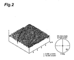
- the surface of the GaN single-crystal substrate 11 is flattened, so as to attain a mirror surface state. When observed under a microscope, however, fine damages formed by mechanical polishing are seen on the surface of the substrate 11.
- a surface image of the polished GaN single-crystal substrate 11 observed under an atomic force microscope is shown in Fig. 2. As depicted, a number of minute defects caused by polishing are seen on the substrate 11. The root-mean-square roughness (Rms) of this surface is about 1.0 nm.
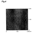
- Fig. 4 shows a typical surface observation image of the GaN single-crystal substrate flattened by the foregoing heat treatment.
- the substrate 11 shown in Fig. 4 is a substrate heat-treated under the condition with a substrate temperature (T1) of 1020°C and a time (t1) of 10 minutes in an atmosphere of mixed gas G1.
- T1 substrate temperature
- t1 time
- This substrate surface exhibited an Rms of about 0.19 nm, whereas a step-and-terrace structure corresponding to one atomic layer was observed. Namely, such heat treatment allowed the surface of the GaN single-crystal substrate 11 to exhibit an Rms of 0.2 nm or less.
- the reaction rate of expression (1) is so slow that only a few % of NH 3 can decompose into H 2 and N 2 even at 1000°C.
- Such an amount of H 2 is insufficient for the above-mentioned surface heat treatment step to progress, whereby it is preferred that an H 2 gas be added to the mixed gas G1. Therefore, it is preferable for the surface heat treatment step to be carried out in an atmosphere of a mixed gas comprising NH 3 and H 2 gases.
- the heat treatment temperature affects the rate of each of the above-mentioned reactions, the length of Ga atom migration, the rate of Ga atom desorption, and the like. Namely, as the substrate temperature T1 is higher, the Ga migration length becomes longer, whereby Ga atoms are more likely to reach the polish-damaged parts (recesses). When the substrate temperature T1 is low, by contrast, Ga atoms react with NH 3 to yield GaN before reaching the polish-damaged parts, so as to generate nuclei, thus failing to flatten the surface. Assuming the surface to be flattened in such a mechanism, the inventors diligently studied temperatures suitable therefor and, as a result, have found that the substrate temperature T1 is preferably 1020°C or higher. Therefore, in the surface heat treatment step, the substrate temperature T1 is preferably at least 1020°C.
- the time required for flattening the surface of the substrate 11 is a time by which the polish-damaged parts are sufficiently filled due to the Ga atom migration and GaN generation.
- the inventors have found that, though depending on the polishing state of substrate 11, the surface of the substrate 11 can be flattened by heat treatment of at least 10 minutes for the surface roughness with an Rms of about 1.0 nm finished by mechanical polishing in general. Namely, the heat treatment time is preferably at least 10 minutes.
- the GaN single-crystal substrate 11 be kept from being exposed to atmosphere before epitaxial growth after the heat treatment. This is because of the fact that, when exposed to the atmosphere, the surface of the substrate 11 may get oxidized or absorb organic matters and other contaminants, thereby adversely affecting the subsequent epitaxial growth. In this case, it is necessary to carry out surface treatment for purifying the surface of the substrate 11 again before the epitaxial growth, which increases the number of steps. This indicates that epitaxially growing the nitride type compound semiconductor layer 12 on the heat-treated GaN single-crystal substrate 11 can make the epitaxial substrate 10 having a high quality.
- the nitride type compound semiconductor layer 12 is preferably GaN in particular, since its lattice constant coincides with that of the GaN single-crystal substrate 11, so that no misfit dislocation occurs in the interface, thus yielding no fear of deteriorating the crystallinity of the nitride type compound semiconductor layer 12.
- making the epitaxial substrate 11 exhibiting a very flat surface Rms of 0.2 nm or less as an index for the high quality of the epitaxial layer 12 is advantageous in keeping the surface flatness in its subsequent device structure growth, and is effective in improving the yields of light-emitting devices such as light-emitting diodes and laser diodes such as bipolar transistors and field-effect transistors.
- the above-mentioned surface heat treatment step can reduce the crystal axis fluctuation of the epitaxial layer 12. More specifically, the x-ray diffraction half width of the nitride type compound semiconductor layer 12 becomes 100 seconds or less. Namely, the surface of the epitaxial substrate 12 becomes flat, whereby the epitaxial substrate having a favorable crystallinity can be obtained.
- the above-mentioned surface heat treatment can suppress the threading dislocation density of the epitaxial layer 12 to 1 ⁇ 10 6 cm -2 or less. This can suppress the threading dislocation density of a semiconductor layer laminated on the epitaxial layer 12.
- the crystallinity of the epitaxial layer 12 improves while the crystal defects on the surface decrease, whereby the crystallinity of a semiconductor layer laminated on the epitaxial layer 12 becomes favorable, and crystal defects can be restrained from occurring within the semiconductor layer. Therefore, using the epitaxial substrate 10 formed with the epitaxial layer 12 is effective in improving the characteristics, reliabilities, and yields of light-emitting devices such as light-emitting diodes and laser diodes, electronic devices such as bipolar transistors and field-effect transistors, and the like.
- the conductivity of the epitaxial layer (not depicted) formed on the epitaxial substrate 10 can be controlled in conformity to structures of various conductive devices.
- light-emitting devices such as LED and LD can be made by preparing an epitaxial substrate 10 in which an n-type GaN layer 12 is grown on an n-type single-crystal substrate 11, and then growing thereon a basic structure comprising an n-type cladding layer, an active layer, a p-type cladding layer, and a p-type contact layer. Thereafter, such steps as forming an electrode, connecting current terminals, forming a reflecting surface in the case of a laser diode, and so forth are taken as a matter of course, so as to accomplish a device.
- n-type GaN substrate 11 for an npn-type bipolar transistor device, whereas a semi-insulating GaN substrate is preferable for a field-effect transistor.
- a growth method employed for epitaxial growth can be selected from OMVPE, HVPE, MBE, and the like. When any of them is chosen, the GaN single-crystal substrate 11 is heat-treated within an apparatus for growth and then, without taking out the GaN single-crystal substrate 11, the nitride type compound semiconductor layer 12 is epitaxially grown thereon, whereby the surface of the substrate 11 is kept from being contaminated. Therefore, the surface processing step required when the surface is oxidized or contaminated is unnecessary, whereby a high-quality epitaxial substrate can be made easily.
- the GaN substrate 11 was heat-treated in an OMVPE apparatus under various conditions. Further, the GaN layer 12 was epitaxially grown within the same apparatus .
- the OMVPE apparatus 20 used comprises a vertical growth furnace (reaction chamber) 22 constructed so as to jet out material gases at right angles with respect to the surface of the substrate 11.
- the growth furnace 22 is mainly constituted by material supply pipes 21a to 21e for supplying material gases and carrier gases, an exhaust pipe 23o for letting out the remainder gases after growth, a sample table 32 for placing a plurality of substrates 11, and heaters 33 for heating the sample table 32 from thereunder.
- a water-cooling jacket 34 is disposed in the upper part within the growth furnace 22, so as to be able to prevent the material gases from being heated to react with each other before reaching the substrate 11.
- the driving mechanism 40 Disposed under the growth furnace 22 is a driving mechanism 40 for rotating the sample table 32.
- the driving mechanism 40 comprises a motor 41, and a rotary shaft 43 to which the rotation of the motor 41 is transmitted by way of a belt 42.
- the rotary shaft 43 is introduced into the growth furnace 22 by way of a magnetic fluid seal 44, such that its upper end is connected to the bottom face of the sample table 32.
- the magnetic fluid seal 44 disposed about the rotary shaft 43 tightly closes the through hole of the growth furnace 22 through which the rotary shaft 43 is inserted.
- the sample table 32 for which SiC-coated carbon can be used, is driven by the driving mechanism 40 at a high speed of about 1000 rpm, for example.
- NH 3 was 11 slm
- H 2 or N 2 was 5 slm.
- the condition at the time of growing GaN was such that the substrate temperature was 1000°C, ammonia was 11 slm, H 2 was 5 slm, trimethyl gallium was 180 to 400 ⁇ mol/min, and the pressure was about 27 kPa (i.e., 200 Torr).
- a GaN/sapphire substrate using sapphire as a substrate with a GaN layer grown beforehand was grown at the same time.
- Table 1 shows the results of observation of the surface of the substrate 11 under an atomic force microscope after the heat treatment
- Table 2 shows the results of evaluation by the atomic force microscope and x-ray diffraction of samples having grown the GaN layer 12 by 2 ⁇ m.
- the x-ray diffraction was evaluated by the respective ⁇ scan half width values of the (0002) reflection indicative of the c-axis fluctuation and the (10-11) reflection indicative of both of the fluctuations of c- and a-axes.
- Table 1 indicates that the flatness and surface roughness are not improved upon heat treatment at a substrate temperature of less than 1020°C, whereas flat, favorable GaN single-crystal substrates with a low roughness can be made when heat treatment is carried out for at least 10 minutes at a substrate temperature of 1020°C or higher in a mixed atmosphere of NH 3 and H 2 .
- Table 2 indicates that both the surface roughness and x-ray diffraction are large in the comparative example on sapphire, but are remarkably improved when a GaN substrate is used.
- heat treatment for 10 minutes at a substrate temperature of 1020°C or higher in a mixed atmosphere of NH 3 and H 2 can greatly improve the surface roughness and crystal axis fluctuation of the epitaxial layer.
- the heat treatment in the atmosphere of NH 3 + N 2 is unfavorable, since the surface roughness (Rms) may exceed 0.2 nm or the x-ray diffraction half width may exceed 100 seconds.
- Table 2 does not measure the surface roughness (Rms) after the heat treatment, the heat treatment condition under which the surface roughness and crystal axis fluctuation of the epitaxial layer become sufficiently small coincides with the condition under which the surface roughness after heat treatment becomes 0.2 nm or less. Namely, for attaining a favorable epitaxial layer, a GaN single-crystal substrate having a surface roughness of 0.2 nm or less must be used.
- the threading dislocation density was determined from pit-like defects observed under an atomic force microscope in practice, it was about 10 8 to 10 9 cm -2 in the epitaxial layer grown on the sapphire substrate, but was 10 6 cm -2 or less and thus was favorable in the epitaxial layer 12 grown on the GaN substrate 11 in many samples.
- the present invention can reduce the surface roughness of the GaN single-crystal, thus being able to provide a GaN single-crystal substrate suitable for epitaxial growth.
- a nitride type compound semiconductor layer is epitaxially grown on the GaN single-crystal substrate of the present invention, a nitride type compound semiconductor device exhibiting favorable characteristics can be formed.
Landscapes
- Chemical & Material Sciences (AREA)
- Organic Chemistry (AREA)
- Engineering & Computer Science (AREA)
- Crystallography & Structural Chemistry (AREA)
- Materials Engineering (AREA)
- Metallurgy (AREA)
- Inorganic Chemistry (AREA)
- Chemical Kinetics & Catalysis (AREA)
- General Chemical & Material Sciences (AREA)
- Led Devices (AREA)
- Crystals, And After-Treatments Of Crystals (AREA)
- Semiconductor Lasers (AREA)
- Mechanical Treatment Of Semiconductor (AREA)
Priority Applications (1)
| Application Number | Priority Date | Filing Date | Title |
|---|---|---|---|
| EP11195922A EP2437286A1 (de) | 2002-05-13 | 2003-05-13 | GaN-einkristallines Substrat |
Applications Claiming Priority (2)
| Application Number | Priority Date | Filing Date | Title |
|---|---|---|---|
| JP2002137722 | 2002-05-13 | ||
| JP2002137722A JP2003327497A (ja) | 2002-05-13 | 2002-05-13 | GaN単結晶基板、窒化物系半導体エピタキシャル基板、窒化物系半導体素子及びその製造方法 |
Publications (2)
| Publication Number | Publication Date |
|---|---|
| EP1363322A2 true EP1363322A2 (de) | 2003-11-19 |
| EP1363322A3 EP1363322A3 (de) | 2009-10-21 |
Family
ID=29267760
Family Applications (2)
| Application Number | Title | Priority Date | Filing Date |
|---|---|---|---|
| EP11195922A Withdrawn EP2437286A1 (de) | 2002-05-13 | 2003-05-13 | GaN-einkristallines Substrat |
| EP03009850A Ceased EP1363322A3 (de) | 2002-05-13 | 2003-05-13 | GaN-einkristallines Substrat, epitaktisches Nitrid-Typ-Halbleitersubstrat, Nitrid-Typ-Halbleitervorrichtung und Verfahren zu deren Herstellung |
Family Applications Before (1)
| Application Number | Title | Priority Date | Filing Date |
|---|---|---|---|
| EP11195922A Withdrawn EP2437286A1 (de) | 2002-05-13 | 2003-05-13 | GaN-einkristallines Substrat |
Country Status (7)
| Country | Link |
|---|---|
| US (3) | US6841274B2 (de) |
| EP (2) | EP2437286A1 (de) |
| JP (1) | JP2003327497A (de) |
| KR (2) | KR20030088336A (de) |
| CN (1) | CN100337308C (de) |
| SG (1) | SG112879A1 (de) |
| TW (1) | TWI271788B (de) |
Cited By (2)
| Publication number | Priority date | Publication date | Assignee | Title |
|---|---|---|---|---|
| WO2013060949A1 (fr) * | 2011-10-27 | 2013-05-02 | Commissariat A L'energie Atomique Et Aux Energies Alternatives | Procédé de lissage d'une surface par traitement thermique |
| EP2821532A4 (de) * | 2013-03-29 | 2015-10-07 | Ngk Insulators Ltd | Verfahren zur verarbeitung von gruppe-iii-nitrid-substraten und verfahren zur herstellung epitaktischer substrate |
Families Citing this family (60)
| Publication number | Priority date | Publication date | Assignee | Title |
|---|---|---|---|---|
| US6596079B1 (en) * | 2000-03-13 | 2003-07-22 | Advanced Technology Materials, Inc. | III-V nitride substrate boule and method of making and using the same |
| US7105865B2 (en) | 2001-09-19 | 2006-09-12 | Sumitomo Electric Industries, Ltd. | AlxInyGa1−x−yN mixture crystal substrate |
| JP3801125B2 (ja) * | 2001-10-09 | 2006-07-26 | 住友電気工業株式会社 | 単結晶窒化ガリウム基板と単結晶窒化ガリウムの結晶成長方法および単結晶窒化ガリウム基板の製造方法 |
| US7354477B2 (en) * | 2001-10-09 | 2008-04-08 | Sumitomo Electric Industries, Ltd. | Method of growing GaN crystal, method of producing single crystal GaN substrate, and single crystal GaN substrate |
| US7303630B2 (en) * | 2003-11-05 | 2007-12-04 | Sumitomo Electric Industries, Ltd. | Method of growing GaN crystal, method of producing single crystal GaN substrate, and single crystal GaN substrate |
| JP2003327497A (ja) * | 2002-05-13 | 2003-11-19 | Sumitomo Electric Ind Ltd | GaN単結晶基板、窒化物系半導体エピタキシャル基板、窒化物系半導体素子及びその製造方法 |
| US9279193B2 (en) * | 2002-12-27 | 2016-03-08 | Momentive Performance Materials Inc. | Method of making a gallium nitride crystalline composition having a low dislocation density |
| KR20060024772A (ko) * | 2003-06-16 | 2006-03-17 | 스미토모덴키고교가부시키가이샤 | 질화물 반도체 결정 표면의 가공 방법 및 그 방법에 의해얻어진 질화물 반도체 결정 |
| US7510641B2 (en) * | 2003-07-21 | 2009-03-31 | Los Alamos National Security, Llc | High current density electropolishing in the preparation of highly smooth substrate tapes for coated conductors |
| US7118813B2 (en) * | 2003-11-14 | 2006-10-10 | Cree, Inc. | Vicinal gallium nitride substrate for high quality homoepitaxy |
| JP4622447B2 (ja) * | 2004-01-23 | 2011-02-02 | 住友電気工業株式会社 | Iii族窒化物結晶基板の製造方法 |
| JP2005217374A (ja) * | 2004-02-02 | 2005-08-11 | Sumitomo Electric Ind Ltd | 化合物半導体素子の製造方法 |
| US7187059B2 (en) * | 2004-06-24 | 2007-03-06 | International Business Machines Corporation | Compressive SiGe <110> growth and structure of MOSFET devices |
| TWI408263B (zh) * | 2004-07-01 | 2013-09-11 | 住友電氣工業股份有限公司 | AlxGayIn1-x-yN基板、AlxGayIn1-x-yN基板之清潔方法、AlN基板及AlN基板之清潔方法 |
| WO2006014421A2 (en) * | 2004-07-06 | 2006-02-09 | The Regents Of The University Of California | METHOD FOR WAFER BONDING (Al, In, Ga)N AND Zn(S, Se) FOR OPTOELECTRONIC APPLICATIONS |
| JP2006032737A (ja) * | 2004-07-16 | 2006-02-02 | Koha Co Ltd | 発光素子 |
| JP4575745B2 (ja) * | 2004-10-18 | 2010-11-04 | 株式会社豊田中央研究所 | GaN系半導体層に上部層が積層されている半導体装置の製造方法 |
| JP3816942B2 (ja) | 2004-10-27 | 2006-08-30 | 三菱電機株式会社 | 半導体素子の製造方法 |
| CN101452837B (zh) * | 2004-10-27 | 2011-04-20 | 三菱电机株式会社 | 半导体元件的制造方法 |
| JP4432827B2 (ja) | 2005-04-26 | 2010-03-17 | 住友電気工業株式会社 | Iii族窒化物半導体素子およびエピタキシャル基板 |
| JP4872246B2 (ja) * | 2005-06-10 | 2012-02-08 | 住友電気工業株式会社 | 半絶縁性GaAs基板及びエピタキシャル基板 |
| US9708735B2 (en) | 2005-06-23 | 2017-07-18 | Sumitomo Electric Industries, Ltd. | Group III nitride crystal substrate, epilayer-containing group III nitride crystal substrate, semiconductor device and method of manufacturing the same |
| JP4277826B2 (ja) | 2005-06-23 | 2009-06-10 | 住友電気工業株式会社 | 窒化物結晶、窒化物結晶基板、エピ層付窒化物結晶基板、ならびに半導体デバイスおよびその製造方法 |
| US8771552B2 (en) * | 2005-06-23 | 2014-07-08 | Sumitomo Electric Industries, Ltd. | Group III nitride crystal substrate, epilayer-containing group III nitride crystal substrate, semiconductor device and method of manufacturing the same |
| WO2007008394A1 (en) * | 2005-07-11 | 2007-01-18 | Cree, Inc. | Laser diode orientation on mis-cut substrates |
| KR100695119B1 (ko) * | 2006-01-20 | 2007-03-14 | 삼성코닝 주식회사 | GaN 기판의 제조방법 |
| US9406505B2 (en) * | 2006-02-23 | 2016-08-02 | Allos Semiconductors Gmbh | Nitride semiconductor component and process for its production |
| EP2016614A4 (de) * | 2006-04-25 | 2014-04-09 | Univ Singapore | Verfahren eines auf der epitaxialen lateral-überwachstums-galliumnitrid vorlage gewachsenen zinkoxidfilms |
| JP4714087B2 (ja) * | 2006-06-14 | 2011-06-29 | 住友電気工業株式会社 | GaN基板の保存方法、および半導体デバイスの製造方法 |
| US8476158B2 (en) | 2006-06-14 | 2013-07-02 | Sumitomo Electric Industries, Ltd. | Method of preparing and storing GaN substrate, prepared and stored GaN substrate, and semiconductor device and method of its manufacture |
| US7755103B2 (en) | 2006-08-03 | 2010-07-13 | Sumitomo Electric Industries, Ltd. | Nitride gallium semiconductor substrate and nitride semiconductor epitaxial substrate |
| JP4940928B2 (ja) * | 2006-12-15 | 2012-05-30 | 日立電線株式会社 | 窒化物半導体の製造方法 |
| JP4259591B2 (ja) * | 2007-01-16 | 2009-04-30 | 住友電気工業株式会社 | Iii族窒化物結晶の製造方法、iii族窒化物結晶基板およびiii族窒化物半導体デバイス |
| JP5298470B2 (ja) * | 2007-07-11 | 2013-09-25 | 三菱電機株式会社 | 半導体装置、半導体装置の製造方法 |
| FR2921200B1 (fr) * | 2007-09-18 | 2009-12-18 | Centre Nat Rech Scient | Heterostructures semi-conductrices monolithiques epitaxiees et leur procede de fabrication |
| US7824929B2 (en) | 2007-10-22 | 2010-11-02 | Toyoda Gosei Co., Ltd. | Method for producing group III nitride-based compound semiconductor |
| JP5223112B2 (ja) * | 2007-10-22 | 2013-06-26 | 豊田合成株式会社 | Iii族窒化物系化合物半導体の製造方法 |
| JP4924498B2 (ja) * | 2008-03-18 | 2012-04-25 | 住友電気工業株式会社 | 窒化物系半導体発光素子、エピタキシャルウエハ、及び窒化物系半導体発光素子を作製する方法 |
| US20090309127A1 (en) * | 2008-06-13 | 2009-12-17 | Soraa, Inc. | Selective area epitaxy growth method and structure |
| US8847249B2 (en) * | 2008-06-16 | 2014-09-30 | Soraa, Inc. | Solid-state optical device having enhanced indium content in active regions |
| JP5173673B2 (ja) * | 2008-08-22 | 2013-04-03 | スタンレー電気株式会社 | 半導体発光素子 |
| JP4917585B2 (ja) * | 2008-08-26 | 2012-04-18 | 住友電気工業株式会社 | 窒化物系半導体光素子を製造する方法、及びエピタキシャルウエハを製造する方法 |
| WO2010150809A1 (ja) | 2009-06-24 | 2010-12-29 | 日亜化学工業株式会社 | 窒化物半導体発光ダイオード |
| JP2011011942A (ja) * | 2009-07-01 | 2011-01-20 | Hitachi Kokusai Electric Inc | 結晶製造装置及び結晶製造方法 |
| US9583678B2 (en) | 2009-09-18 | 2017-02-28 | Soraa, Inc. | High-performance LED fabrication |
| JP2012142444A (ja) * | 2010-12-28 | 2012-07-26 | Sharp Corp | 発光デバイス、透明導電膜の形成方法、発光デバイスの製造方法および電気機器 |
| US9236530B2 (en) | 2011-04-01 | 2016-01-12 | Soraa, Inc. | Miscut bulk substrates |
| JP2012231103A (ja) | 2011-04-15 | 2012-11-22 | Mitsubishi Chemicals Corp | Iii族窒化物結晶の製造方法およびiii族窒化物結晶 |
| US8686431B2 (en) | 2011-08-22 | 2014-04-01 | Soraa, Inc. | Gallium and nitrogen containing trilateral configuration for optical devices |
| US9646827B1 (en) * | 2011-08-23 | 2017-05-09 | Soraa, Inc. | Method for smoothing surface of a substrate containing gallium and nitrogen |
| JP6047995B2 (ja) * | 2012-08-22 | 2016-12-21 | 住友電気工業株式会社 | Iii族窒化物半導体を作製する方法、半導体素子を作製する方法、iii族窒化物半導体装置、熱処理を行う方法 |
| CN108281378B (zh) * | 2012-10-12 | 2022-06-24 | 住友电气工业株式会社 | Iii族氮化物复合衬底、半导体器件及它们的制造方法 |
| FR3010228B1 (fr) | 2013-08-30 | 2016-12-30 | St Microelectronics Tours Sas | Procede de traitement d'une couche de nitrure de gallium comportant des dislocations |
| US9627197B2 (en) * | 2014-04-15 | 2017-04-18 | Globalwafers Co., Ltd. | Composite substrate, semiconductor device including the same, and method of manufacturing the same |
| KR20150138479A (ko) | 2014-05-29 | 2015-12-10 | 삼성전자주식회사 | 발광 소자 패키지의 제조 방법 |
| WO2017090279A1 (ja) * | 2015-11-24 | 2017-06-01 | 住友電気工業株式会社 | 炭化珪素単結晶基板、炭化珪素エピタキシャル基板および炭化珪素半導体装置の製造方法 |
| JP6531691B2 (ja) * | 2016-03-24 | 2019-06-19 | 豊田合成株式会社 | 縦型トレンチmosfetの製造方法 |
| CN107221496B (zh) * | 2017-05-26 | 2020-04-24 | 东莞市中镓半导体科技有限公司 | 一种氮化物材料激光剥离后的表面处理方法 |
| US11767612B2 (en) | 2017-09-22 | 2023-09-26 | Tokuyama Corporation | Group III nitride single crystal substrate |
| CN111681948A (zh) * | 2020-06-12 | 2020-09-18 | 中国科学院长春光学精密机械与物理研究所 | 一种图形化衬底及其制备方法 |
Family Cites Families (25)
| Publication number | Priority date | Publication date | Assignee | Title |
|---|---|---|---|---|
| US5252175A (en) * | 1990-06-29 | 1993-10-12 | The United States Of America As Represented By The Secretary Of The Air Force | Capillary pressure relief for magnetic Kyropoulos growth of semiconductor crystals |
| GB9214479D0 (en) * | 1992-07-08 | 1992-08-19 | Atomic Energy Authority Uk | Pressure transducers |
| US5679152A (en) * | 1994-01-27 | 1997-10-21 | Advanced Technology Materials, Inc. | Method of making a single crystals Ga*N article |
| US5679153A (en) * | 1994-11-30 | 1997-10-21 | Cree Research, Inc. | Method for reducing micropipe formation in the epitaxial growth of silicon carbide and resulting silicon carbide structures |
| JP3164016B2 (ja) * | 1996-05-31 | 2001-05-08 | 住友電気工業株式会社 | 発光素子および発光素子用ウエハの製造方法 |
| GB2323209A (en) * | 1997-03-13 | 1998-09-16 | Sharp Kk | Molecular beam epitaxy apparatus and method |
| US6117499A (en) * | 1997-04-09 | 2000-09-12 | Komag, Inc. | Micro-texture media made by polishing of a selectively irradiated surface |
| JPH10335750A (ja) * | 1997-06-03 | 1998-12-18 | Sony Corp | 半導体基板および半導体装置 |
| CA2311132C (en) * | 1997-10-30 | 2004-12-07 | Sumitomo Electric Industries, Ltd. | Gan single crystalline substrate and method of producing the same |
| US6087217A (en) * | 1997-11-05 | 2000-07-11 | Taiwan Semiconductor Manufacturing Company, Ltd. | Method for improving capacitance in DRAM capacitors and devices formed |
| US6146468A (en) * | 1998-06-29 | 2000-11-14 | Speedfam-Ipec Corporation | Semiconductor wafer treatment |
| JP2000049114A (ja) * | 1998-07-30 | 2000-02-18 | Sony Corp | 電極およびその形成方法ならびに半導体装置およびその製造方法 |
| KR100277968B1 (ko) * | 1998-09-23 | 2001-03-02 | 구자홍 | 질화갈륨 기판 제조방법 |
| US6372041B1 (en) * | 1999-01-08 | 2002-04-16 | Gan Semiconductor Inc. | Method and apparatus for single crystal gallium nitride (GaN) bulk synthesis |
| KR100304664B1 (ko) * | 1999-02-05 | 2001-09-26 | 윤종용 | GaN막 제조 방법 |
| US6592663B1 (en) * | 1999-06-09 | 2003-07-15 | Ricoh Company Ltd. | Production of a GaN bulk crystal substrate and a semiconductor device formed on a GaN bulk crystal substrate |
| GB2350927A (en) * | 1999-06-12 | 2000-12-13 | Sharp Kk | A method growing nitride semiconductor layer by molecular beam epitaxy |
| JP3393469B2 (ja) * | 1999-07-15 | 2003-04-07 | 日本電気株式会社 | 薄膜半導体素子の製造方法及び薄膜半導体形成装置 |
| JP2001144014A (ja) * | 1999-11-17 | 2001-05-25 | Ngk Insulators Ltd | エピタキシャル成長用基板およびその製造方法 |
| US6447604B1 (en) * | 2000-03-13 | 2002-09-10 | Advanced Technology Materials, Inc. | Method for achieving improved epitaxy quality (surface texture and defect density) on free-standing (aluminum, indium, gallium) nitride ((al,in,ga)n) substrates for opto-electronic and electronic devices |
| US6596079B1 (en) * | 2000-03-13 | 2003-07-22 | Advanced Technology Materials, Inc. | III-V nitride substrate boule and method of making and using the same |
| GB2363518A (en) * | 2000-06-17 | 2001-12-19 | Sharp Kk | A method of growing a nitride layer on a GaN substrate |
| US6488767B1 (en) * | 2001-06-08 | 2002-12-03 | Advanced Technology Materials, Inc. | High surface quality GaN wafer and method of fabricating same |
| US6648966B2 (en) * | 2001-08-01 | 2003-11-18 | Crystal Photonics, Incorporated | Wafer produced thereby, and associated methods and devices using the wafer |
| JP2003327497A (ja) * | 2002-05-13 | 2003-11-19 | Sumitomo Electric Ind Ltd | GaN単結晶基板、窒化物系半導体エピタキシャル基板、窒化物系半導体素子及びその製造方法 |
-
2002
- 2002-05-13 JP JP2002137722A patent/JP2003327497A/ja active Pending
-
2003
- 2003-04-30 SG SG200302475A patent/SG112879A1/en unknown
- 2003-05-08 US US10/431,431 patent/US6841274B2/en not_active Expired - Lifetime
- 2003-05-10 KR KR10-2003-0029615A patent/KR20030088336A/ko not_active Ceased
- 2003-05-13 EP EP11195922A patent/EP2437286A1/de not_active Withdrawn
- 2003-05-13 TW TW092113001A patent/TWI271788B/zh not_active IP Right Cessation
- 2003-05-13 EP EP03009850A patent/EP1363322A3/de not_active Ceased
- 2003-05-13 CN CNB031251633A patent/CN100337308C/zh not_active Expired - Fee Related
-
2004
- 2004-11-29 US US10/997,887 patent/US20050095861A1/en not_active Abandoned
-
2010
- 2010-03-16 US US12/725,233 patent/US20100173483A1/en not_active Abandoned
- 2010-07-19 KR KR1020100069704A patent/KR20100089049A/ko not_active Ceased
Non-Patent Citations (2)
| Title |
|---|
| TOMIYA S. ET AL, PHYSICA STATUS SOLIDI A WILEY-VCH GERMANY, VOL. 188, NR. 1, PAGE(S) 69 - 72, ISSN: 0031-8965 * |
| TOMIYA S. ET AL: "Dislocation Related Issues in the Degradation of GaN-Based Laser Diodes", IEEE JOURNAL OF SELECTED TOPICS IN QUANTUM ELECTRONICS, IEEE SERVICE CENTER, PISCATAWAY, NJ, US, vol. 10, no. 6, 1 November 2004 (2004-11-01), pages 1277 - 1286, XP011126352, ISSN: 1077-260X, DOI: 10.1109/JSTQE.2004.837735 * |
Cited By (5)
| Publication number | Priority date | Publication date | Assignee | Title |
|---|---|---|---|---|
| WO2013060949A1 (fr) * | 2011-10-27 | 2013-05-02 | Commissariat A L'energie Atomique Et Aux Energies Alternatives | Procédé de lissage d'une surface par traitement thermique |
| FR2982071A1 (fr) * | 2011-10-27 | 2013-05-03 | Commissariat Energie Atomique | Procede de lissage d'une surface par traitement thermique |
| US8962496B2 (en) | 2011-10-27 | 2015-02-24 | Commissariat A L'energie Atomique Et Aux Energies Alternatives | Process for smoothing a surface via heat treatment |
| EP2821532A4 (de) * | 2013-03-29 | 2015-10-07 | Ngk Insulators Ltd | Verfahren zur verarbeitung von gruppe-iii-nitrid-substraten und verfahren zur herstellung epitaktischer substrate |
| US9196480B2 (en) | 2013-03-29 | 2015-11-24 | Ngk Insulators, Ltd. | Method for treating group III nitride substrate and method for manufacturing epitaxial substrate |
Also Published As
| Publication number | Publication date |
|---|---|
| US20100173483A1 (en) | 2010-07-08 |
| US6841274B2 (en) | 2005-01-11 |
| TWI271788B (en) | 2007-01-21 |
| SG112879A1 (en) | 2005-07-28 |
| TW200405429A (en) | 2004-04-01 |
| US20030209185A1 (en) | 2003-11-13 |
| US20050095861A1 (en) | 2005-05-05 |
| CN100337308C (zh) | 2007-09-12 |
| EP1363322A3 (de) | 2009-10-21 |
| EP2437286A1 (de) | 2012-04-04 |
| CN1462060A (zh) | 2003-12-17 |
| KR20030088336A (ko) | 2003-11-19 |
| JP2003327497A (ja) | 2003-11-19 |
| KR20100089049A (ko) | 2010-08-11 |
Similar Documents
| Publication | Publication Date | Title |
|---|---|---|
| US6841274B2 (en) | GaN single-crystal substrate, nitride type semiconductor epitaxial substrate, nitride type semiconductor device, and methods of making the same | |
| JP5607781B2 (ja) | 大面積で均一な低転位密度GaN基板およびその製造プロセス | |
| US6943095B2 (en) | Low defect density (Ga, A1, In) N and HVPE process for making same | |
| US9431489B2 (en) | β-Ga2O3-based single crystal substrate | |
| JP5108641B2 (ja) | GaN単結晶基板、窒化物系半導体エピタキシャル基板、及び、窒化物系半導体素子 | |
| JPH0856015A (ja) | 半導体薄膜の形成方法 | |
| CN103748662B (zh) | 半导体衬底及形成方法 | |
| Weeks Jr et al. | Undoped and doped GaN thin films deposited on high-temperature monocrystalline AlN buffer layers on vicinal and on-axis α (6H)–SiC (0001) substrates via organometallic vapor phase epitaxy | |
| JP4633962B2 (ja) | 窒化物半導体基板の製造方法 | |
| JP3353527B2 (ja) | 窒化ガリウム系半導体の製造方法 | |
| JP3658756B2 (ja) | 化合物半導体の製造方法 | |
| JP4852795B2 (ja) | 化合物半導体の製造方法 | |
| JPH09129651A (ja) | サファイア基板のサーマル・アニーリング方法及び装置 | |
| JP2000340509A (ja) | GaN基板およびその製造方法 | |
| JP2004307253A (ja) | 半導体基板の製造方法 | |
| US20100064966A1 (en) | Method of growing zinc-oxide-based semiconductor and method of manufacturing semiconductor light emitting device | |
| JP2004035360A (ja) | GaN単結晶基板、窒化物系半導体エピタキシャル基板及びその製造方法 | |
| JP2004165564A (ja) | 窒化ガリウム結晶基板の製造方法と窒化ガリウム結晶基板及びそれを備えた窒化ガリウム系半導体素子 | |
| WO2003056073A1 (en) | Group iii nitride semiconductor substrate and its manufacturing method | |
| US20060255339A1 (en) | Single-crystalline gallium nitride substrate | |
| JP2677221B2 (ja) | 窒化物系iii−v族化合物半導体結晶の成長方法 | |
| Tavernier et al. | Progress Toward Making Gallium Nitride Seed Crystals Using Hydride Vapor‐Phase Epitaxy | |
| JP2005217374A (ja) | 化合物半導体素子の製造方法 | |
| JP2000164511A (ja) | 窒化物半導体堆積基板 | |
| JP2005033132A (ja) | GaN基板の製造方法 |
Legal Events
| Date | Code | Title | Description |
|---|---|---|---|
| PUAI | Public reference made under article 153(3) epc to a published international application that has entered the european phase |
Free format text: ORIGINAL CODE: 0009012 |
|
| AK | Designated contracting states |
Kind code of ref document: A2 Designated state(s): AT BE BG CH CY CZ DE DK EE ES FI FR GB GR HU IE IT LI LU MC NL PT RO SE SI SK TR |
|
| AX | Request for extension of the european patent |
Extension state: AL LT LV MK |
|
| PUAL | Search report despatched |
Free format text: ORIGINAL CODE: 0009013 |
|
| AK | Designated contracting states |
Kind code of ref document: A3 Designated state(s): AT BE BG CH CY CZ DE DK EE ES FI FR GB GR HU IE IT LI LU MC NL PT RO SE SI SK TR |
|
| AX | Request for extension of the european patent |
Extension state: AL LT LV MK |
|
| RIC1 | Information provided on ipc code assigned before grant |
Ipc: C30B 25/02 20060101ALI20090910BHEP Ipc: C30B 29/40 20060101ALI20090910BHEP Ipc: H01L 21/20 20060101ALI20090910BHEP Ipc: H01L 21/324 20060101AFI20030911BHEP |
|
| 17P | Request for examination filed |
Effective date: 20091119 |
|
| 17Q | First examination report despatched |
Effective date: 20091218 |
|
| AKX | Designation fees paid |
Designated state(s): DE FR GB |
|
| APBK | Appeal reference recorded |
Free format text: ORIGINAL CODE: EPIDOSNREFNE |
|
| APBN | Date of receipt of notice of appeal recorded |
Free format text: ORIGINAL CODE: EPIDOSNNOA2E |
|
| APBR | Date of receipt of statement of grounds of appeal recorded |
Free format text: ORIGINAL CODE: EPIDOSNNOA3E |
|
| APAF | Appeal reference modified |
Free format text: ORIGINAL CODE: EPIDOSCREFNE |
|
| RIN1 | Information on inventor provided before grant (corrected) |
Inventor name: CHEN, PENG Inventor name: CHUA, SOO-JIN Inventor name: TAKASUKA, EIRYO Inventor name: UENO, MASAKI |
|
| APBT | Appeal procedure closed |
Free format text: ORIGINAL CODE: EPIDOSNNOA9E |
|
| STAA | Information on the status of an ep patent application or granted ep patent |
Free format text: STATUS: THE APPLICATION HAS BEEN REFUSED |
|
| 18R | Application refused |
Effective date: 20150603 |