EP1364991A1 - Halbleitende harzzusammensetzung und halbleitendes element - Google Patents
Halbleitende harzzusammensetzung und halbleitendes element Download PDFInfo
- Publication number
- EP1364991A1 EP1364991A1 EP01999610A EP01999610A EP1364991A1 EP 1364991 A1 EP1364991 A1 EP 1364991A1 EP 01999610 A EP01999610 A EP 01999610A EP 01999610 A EP01999610 A EP 01999610A EP 1364991 A1 EP1364991 A1 EP 1364991A1
- Authority
- EP
- European Patent Office
- Prior art keywords
- semiconductive
- resistance
- roller
- relative humidity
- measured
- Prior art date
- Legal status (The legal status is an assumption and is not a legal conclusion. Google has not performed a legal analysis and makes no representation as to the accuracy of the status listed.)
- Withdrawn
Links
- 0 CC(C)(C(C)(*)[U])ON Chemical compound CC(C)(C(C)(*)[U])ON 0.000 description 1
Images



Classifications
-
- C—CHEMISTRY; METALLURGY
- C08—ORGANIC MACROMOLECULAR COMPOUNDS; THEIR PREPARATION OR CHEMICAL WORKING-UP; COMPOSITIONS BASED THEREON
- C08L—COMPOSITIONS OF MACROMOLECULAR COMPOUNDS
- C08L71/00—Compositions of polyethers obtained by reactions forming an ether link in the main chain; Compositions of derivatives of such polymers
- C08L71/02—Polyalkylene oxides
-
- C—CHEMISTRY; METALLURGY
- C08—ORGANIC MACROMOLECULAR COMPOUNDS; THEIR PREPARATION OR CHEMICAL WORKING-UP; COMPOSITIONS BASED THEREON
- C08G—MACROMOLECULAR COMPOUNDS OBTAINED OTHERWISE THAN BY REACTIONS ONLY INVOLVING UNSATURATED CARBON-TO-CARBON BONDS
- C08G65/00—Macromolecular compounds obtained by reactions forming an ether link in the main chain of the macromolecule
- C08G65/02—Macromolecular compounds obtained by reactions forming an ether link in the main chain of the macromolecule from cyclic ethers by opening of the heterocyclic ring
- C08G65/32—Polymers modified by chemical after-treatment
- C08G65/329—Polymers modified by chemical after-treatment with organic compounds
- C08G65/336—Polymers modified by chemical after-treatment with organic compounds containing silicon
-
- G—PHYSICS
- G03—PHOTOGRAPHY; CINEMATOGRAPHY; ANALOGOUS TECHNIQUES USING WAVES OTHER THAN OPTICAL WAVES; ELECTROGRAPHY; HOLOGRAPHY
- G03G—ELECTROGRAPHY; ELECTROPHOTOGRAPHY; MAGNETOGRAPHY
- G03G15/00—Apparatus for electrographic processes using a charge pattern
- G03G15/06—Apparatus for electrographic processes using a charge pattern for developing
- G03G15/08—Apparatus for electrographic processes using a charge pattern for developing using a solid developer, e.g. powder developer
- G03G15/0806—Apparatus for electrographic processes using a charge pattern for developing using a solid developer, e.g. powder developer on a donor element, e.g. belt, roller
- G03G15/0818—Apparatus for electrographic processes using a charge pattern for developing using a solid developer, e.g. powder developer on a donor element, e.g. belt, roller characterised by the structure of the donor member, e.g. surface properties
-
- H—ELECTRICITY
- H01—ELECTRIC ELEMENTS
- H01B—CABLES; CONDUCTORS; INSULATORS; SELECTION OF MATERIALS FOR THEIR CONDUCTIVE, INSULATING OR DIELECTRIC PROPERTIES
- H01B1/00—Conductors or conductive bodies characterised by the conductive materials; Selection of materials as conductors
- H01B1/06—Conductors or conductive bodies characterised by the conductive materials; Selection of materials as conductors mainly consisting of other non-metallic substances
- H01B1/12—Conductors or conductive bodies characterised by the conductive materials; Selection of materials as conductors mainly consisting of other non-metallic substances organic substances
- H01B1/122—Ionic conductors
-
- H—ELECTRICITY
- H01—ELECTRIC ELEMENTS
- H01B—CABLES; CONDUCTORS; INSULATORS; SELECTION OF MATERIALS FOR THEIR CONDUCTIVE, INSULATING OR DIELECTRIC PROPERTIES
- H01B1/00—Conductors or conductive bodies characterised by the conductive materials; Selection of materials as conductors
- H01B1/20—Conductive material dispersed in non-conductive organic material
- H01B1/24—Conductive material dispersed in non-conductive organic material the conductive material comprising carbon-silicon compounds, carbon or silicon
-
- C—CHEMISTRY; METALLURGY
- C08—ORGANIC MACROMOLECULAR COMPOUNDS; THEIR PREPARATION OR CHEMICAL WORKING-UP; COMPOSITIONS BASED THEREON
- C08L—COMPOSITIONS OF MACROMOLECULAR COMPOUNDS
- C08L2203/00—Applications
- C08L2203/20—Applications use in electrical or conductive gadgets
-
- G—PHYSICS
- G03—PHOTOGRAPHY; CINEMATOGRAPHY; ANALOGOUS TECHNIQUES USING WAVES OTHER THAN OPTICAL WAVES; ELECTROGRAPHY; HOLOGRAPHY
- G03G—ELECTROGRAPHY; ELECTROPHOTOGRAPHY; MAGNETOGRAPHY
- G03G2215/00—Apparatus for electrophotographic processes
- G03G2215/08—Details of powder developing device not concerning the development directly
- G03G2215/0855—Materials and manufacturing of the developing device
- G03G2215/0858—Donor member
- G03G2215/0861—Particular composition or materials
Definitions
- the image recording device which applies the electrophotographic method mentioned above include a device in which an intermediate transfer unit is used.
- a static latent image is formed by an image input means on a static latent image carrier which is uniformly charged by a charging means and a toner image is formed by adsorbing the toner particles onto the static latent image.
- the toner image is first transferred to an intermediate transfer unit by the first transfer means and then the toner image formed on the intermediate transfer unit is secondarily transferred to the recording materials such as recording paper by the second transfer means and thereafter, by fixing the toner image on the recording paper, a recorded image is formed.
- the method of adding a metal or metal oxide powder, carbon black or ion conductive materials such as sodium perchlorate is employed for preparing a member of medium resistance by using a high molecular elastomer or foamed material.
- a metal or metal oxide powder or carbon black there is the problem of large fluctuation in position of the resistance and voltage dependency of the electric resistance.
- the nonionic surfactant (E) is preferably a polyoxyethylene compound.
- the member has a resistance of at least 10 5 ⁇ to at most 10 9 ⁇ when measured by applying a direct current voltage of 100 V at 23°C under a relative humidity of 55 %.
- the alkenyl group is introduced to the terminal of polymer (A).
- the cured article obtained by curing the semiconductive composition of the present invention is easy to be brought to the low hardness and high strength.
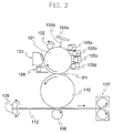
- electrophotographic photoconductor 101 formed by applying photoconductor on an aluminum pipe, is homogeneously charged by charging roller (charger) 102 and then an electrostatic latent image is formed on the surface of the photoconductor by scanning exposure light 104b corresponding with the image data, which is let out from writing device 104a.
- the electrostatic latent image is developed and visualized by developer 105a which corresponds with the color data of electrostatic latent image which was formed.
- This visualized toner image is transferred from electrophotographic photoconductor 101 to the surface of intermediate transfer drum 110 by applying voltage between intermediate transfer drum 110 and photoconductor 101 from an unrepresented power source in transfer area P1 where electrophotographic photoconductor 101 and intermediate transfer drum 110 are in contact.
- the upper limit of the value of R rotate /R static is 1.5 but more preferably is 1.3.
- the lower limit is 0.7 but more preferably is 0.9.
- the deflection of the outer diameter of the member stands for the amount of change in radius of the member and is usually found from the highest value and lowest value of the distance between the base point set to a point away from the member and the exterior surface of the member, which is measured while rotating the member.
- the transferring properties (amount of remnant toner, unevenness in transfer and hollowness of images) of the transfer roller described in Examples and Comparative Examples of Embodiment 5 were evaluated using an intermediate transfer type laser beam printer (device shown in Fig. 2), by output of images under various environments using spherical toner of the 4 colors of cyan (C), magenta (M), yellow (Y) and black (K) having an average particle size of 6 ⁇ m.
- a semiconductive elastic layer was formed on the exterior of the stainless shaft in the same manner as in Comparative Example 5.
- the Asker C hardness of the elastic layer under conditions of a temperature of 21°C and a relative humidity of 60 % was 40 degrees.
- Example 16 After leaving the prepared intermediate transfer drum in an environment of a temperature of 23°C and a relative humidity of 55 % for 24 hours, evaluation was conducted in the same manner as in Example 16.
- R 500 was 1.0 ⁇ 10 8 ⁇
- R 1000 was 9.5 ⁇ 10 7 ⁇
- R 500 /R 1000 was 1.05.
- the resistance of the roller R LL was 2.0 ⁇ 10 8 ⁇
- the resistance of the roller R HH was 6.0 ⁇ 10 7 ⁇
- R LL /R HH was 3.3.
Landscapes
- Chemical & Material Sciences (AREA)
- Physics & Mathematics (AREA)
- Spectroscopy & Molecular Physics (AREA)
- Chemical Kinetics & Catalysis (AREA)
- Health & Medical Sciences (AREA)
- Medicinal Chemistry (AREA)
- Polymers & Plastics (AREA)
- Organic Chemistry (AREA)
- General Chemical & Material Sciences (AREA)
- Dispersion Chemistry (AREA)
- General Physics & Mathematics (AREA)
- Electrostatic Charge, Transfer And Separation In Electrography (AREA)
- Dry Development In Electrophotography (AREA)
Applications Claiming Priority (29)
| Application Number | Priority Date | Filing Date | Title |
|---|---|---|---|
| JP2000373467 | 2000-12-07 | ||
| JP2000373472 | 2000-12-07 | ||
| JP2000373468 | 2000-12-07 | ||
| JP2000373471 | 2000-12-07 | ||
| JP2000373472 | 2000-12-07 | ||
| JP2000373471 | 2000-12-07 | ||
| JP2000373469 | 2000-12-07 | ||
| JP2000373467 | 2000-12-07 | ||
| JP2000373468 | 2000-12-07 | ||
| JP2000373469 | 2000-12-07 | ||
| JP2000394211 | 2000-12-26 | ||
| JP2000394211 | 2000-12-26 | ||
| JP2001004339 | 2001-01-12 | ||
| JP2001004339 | 2001-01-12 | ||
| JP2001029271 | 2001-02-06 | ||
| JP2001029271 | 2001-02-06 | ||
| JP2001033951 | 2001-02-09 | ||
| JP2001033951 | 2001-02-09 | ||
| JP2001085324 | 2001-03-23 | ||
| JP2001085322 | 2001-03-23 | ||
| JP2001085323 | 2001-03-23 | ||
| JP2001085323 | 2001-03-23 | ||
| JP2001085322 | 2001-03-23 | ||
| JP2001085324 | 2001-03-23 | ||
| JP2001089870 | 2001-03-27 | ||
| JP2001089870 | 2001-03-27 | ||
| JP2001103221 | 2001-04-02 | ||
| JP2001103221 | 2001-04-02 | ||
| PCT/JP2001/010604 WO2002046308A1 (en) | 2000-12-07 | 2001-12-05 | Semiconductive resion composition and semiconductive member |
Publications (2)
| Publication Number | Publication Date |
|---|---|
| EP1364991A1 true EP1364991A1 (de) | 2003-11-26 |
| EP1364991A4 EP1364991A4 (de) | 2004-11-17 |
Family
ID=27584947
Family Applications (1)
| Application Number | Title | Priority Date | Filing Date |
|---|---|---|---|
| EP01999610A Withdrawn EP1364991A4 (de) | 2000-12-07 | 2001-12-05 | Halbleitende harzzusammensetzung und halbleitendes element |
Country Status (6)
| Country | Link |
|---|---|
| US (1) | US20040030032A1 (de) |
| EP (1) | EP1364991A4 (de) |
| JP (1) | JPWO2002046308A1 (de) |
| KR (1) | KR20030060971A (de) |
| CN (1) | CN1280351C (de) |
| WO (1) | WO2002046308A1 (de) |
Cited By (4)
| Publication number | Priority date | Publication date | Assignee | Title |
|---|---|---|---|---|
| EP1577713A1 (de) * | 2003-12-12 | 2005-09-21 | Kinyosha Co. Ltd. | Elektrisch leitendes Element mit einer elastischen, ionisch und elektronisch leitenden Schicht und mit einem leitfähigen Pulver hergestellt |
| CN103105762A (zh) * | 2012-12-25 | 2013-05-15 | 深圳市乐普泰科技股份有限公司 | 显影辊及成像装置 |
| CN104115072A (zh) * | 2012-02-17 | 2014-10-22 | 佳能株式会社 | 显影构件、处理盒和电子照相图像形成设备 |
| JP2021103255A (ja) * | 2019-12-25 | 2021-07-15 | 京セラドキュメントソリューションズ株式会社 | 画像形成装置 |
Families Citing this family (24)
| Publication number | Priority date | Publication date | Assignee | Title |
|---|---|---|---|---|
| JP3988641B2 (ja) * | 2002-04-24 | 2007-10-10 | 東海ゴム工業株式会社 | Oa機器部材用ゴム組成物およびそれを用いたoa機器部材 |
| JP4241103B2 (ja) * | 2003-03-10 | 2009-03-18 | 東海ゴム工業株式会社 | 導電性ロールの製法 |
| JP3914511B2 (ja) * | 2003-05-07 | 2007-05-16 | 信越化学工業株式会社 | ロール用ゴム組成物およびそれを用いたイオン導電性ゴムロール |
| JPWO2006038556A1 (ja) * | 2004-10-04 | 2008-05-15 | 株式会社カネカ | 電子写真用弾性ローラ |
| JP4905626B2 (ja) * | 2005-02-15 | 2012-03-28 | 信越化学工業株式会社 | 絶縁性シリコーンゴム組成物及びその硬化物 |
| JP4985911B2 (ja) * | 2006-01-10 | 2012-07-25 | 信越化学工業株式会社 | 導電性フルオロポリエーテル系ゴム組成物 |
| JP4812088B2 (ja) * | 2006-02-24 | 2011-11-09 | キヤノン株式会社 | 帯電部材 |
| JP4865359B2 (ja) * | 2006-02-28 | 2012-02-01 | キヤノン株式会社 | プロセスカートリッジおよび電子写真装置 |
| JP4854326B2 (ja) * | 2006-02-28 | 2012-01-18 | キヤノン株式会社 | 帯電部材、プロセスカートリッジ及び電子写真装置 |
| JP4234751B2 (ja) * | 2006-11-02 | 2009-03-04 | 住友ゴム工業株式会社 | 半導電性ゴムロール |
| US7865091B2 (en) * | 2007-01-10 | 2011-01-04 | Kabushiki Kaisha Toshiba | Image forming apparatus having a transfer surface with elasticity and image forming method |
| JP5501064B2 (ja) * | 2010-03-29 | 2014-05-21 | 富士フイルム株式会社 | 圧力計測用弾性材料、及び、圧力計測装置 |
| JP5825849B2 (ja) * | 2010-06-15 | 2015-12-02 | キヤノン株式会社 | トナーの製造方法 |
| FR2966600B1 (fr) * | 2010-10-21 | 2015-05-01 | Nexans | Dispositif electrique destine a detecter l'humidite |
| JP5611856B2 (ja) * | 2011-02-17 | 2014-10-22 | 株式会社カネカ | 発泡性液状樹脂組成物および発泡体 |
| JP5730122B2 (ja) * | 2011-05-11 | 2015-06-03 | キヤノン株式会社 | 電子写真用ローラ |
| JP5975978B2 (ja) * | 2011-12-19 | 2016-08-23 | キヤノン株式会社 | 帯電部材、電子写真プロセスカートリッジおよび電子写真装置 |
| JP5620950B2 (ja) * | 2012-07-19 | 2014-11-05 | 住友ゴム工業株式会社 | 現像ローラ |
| JP6128108B2 (ja) * | 2014-12-11 | 2017-05-17 | コニカミノルタ株式会社 | 中間転写ベルトおよび画像形成装置 |
| JP6870848B2 (ja) * | 2017-04-28 | 2021-05-12 | 竹本油脂株式会社 | 合成樹脂用導電剤、導電性樹脂組成物及び導電性床材 |
| CN109482093B (zh) * | 2018-11-02 | 2021-04-06 | 中国石油大学(华东) | 一种在微通道中调控不规则气泡形状的方法 |
| CN109433075B (zh) * | 2018-11-02 | 2021-01-08 | 中国石油大学(华东) | 一种在微通道中调控不规则气泡形状的方法 |
| CN114450352B (zh) * | 2019-10-04 | 2023-12-26 | 三键有限公司 | 导电性树脂组合物 |
| JP7815645B2 (ja) * | 2021-08-20 | 2026-02-18 | 富士フイルムビジネスイノベーション株式会社 | 帯電部材、帯電装置、プロセスカートリッジ、及び画像形成装置 |
Family Cites Families (13)
| Publication number | Priority date | Publication date | Assignee | Title |
|---|---|---|---|---|
| US4543390A (en) * | 1984-12-20 | 1985-09-24 | Toray Industries, Inc. | Antistatic resinous compositions |
| JPH03115359A (ja) * | 1989-09-28 | 1991-05-16 | Toray Dow Corning Silicone Co Ltd | イオン導電性材料およびその製造方法 |
| JP3490500B2 (ja) * | 1994-06-28 | 2004-01-26 | 鐘淵化学工業株式会社 | 硬化性導電性組成物 |
| JP3518895B2 (ja) * | 1994-07-28 | 2004-04-12 | 鐘淵化学工業株式会社 | 硬化性導電性組成物 |
| JP3578510B2 (ja) * | 1995-03-31 | 2004-10-20 | 鐘淵化学工業株式会社 | 発泡弾性体層を有するローラーの製法 |
| JP3484873B2 (ja) * | 1996-04-26 | 2004-01-06 | 鐘淵化学工業株式会社 | 現像ローラ |
| KR100317983B1 (ko) * | 1996-04-26 | 2002-06-22 | 후루타 다케시 | 현상롤러_ |
| JP3493902B2 (ja) * | 1996-06-17 | 2004-02-03 | 鐘淵化学工業株式会社 | 現像ローラ |
| JP3493901B2 (ja) * | 1996-06-17 | 2004-02-03 | 鐘淵化学工業株式会社 | 現像ローラ |
| US5810705A (en) * | 1996-08-28 | 1998-09-22 | Kanegafuchi Kagaku Kogyo Kabushiki Kaisha | Developing roller |
| EP1149870A4 (de) * | 1998-08-20 | 2004-12-08 | Kaneka Corp | Zusammensetzung für rolle und rolle daraus |
| JP2000223126A (ja) * | 1999-02-02 | 2000-08-11 | Mitsubishi Paper Mills Ltd | 電極及びその製造方法 |
| JP2000309709A (ja) * | 1999-04-27 | 2000-11-07 | Kanegafuchi Chem Ind Co Ltd | 硬化性導電性組成物およびそれを用いた導電性ゴムローラー |
-
2001
- 2001-12-05 CN CNB018200850A patent/CN1280351C/zh not_active Expired - Fee Related
- 2001-12-05 US US10/432,626 patent/US20040030032A1/en not_active Abandoned
- 2001-12-05 WO PCT/JP2001/010604 patent/WO2002046308A1/ja not_active Ceased
- 2001-12-05 KR KR10-2003-7007404A patent/KR20030060971A/ko not_active Ceased
- 2001-12-05 JP JP2002548036A patent/JPWO2002046308A1/ja active Pending
- 2001-12-05 EP EP01999610A patent/EP1364991A4/de not_active Withdrawn
Non-Patent Citations (2)
| Title |
|---|
| No further relevant documents disclosed * |
| See also references of WO0246308A1 * |
Cited By (8)
| Publication number | Priority date | Publication date | Assignee | Title |
|---|---|---|---|---|
| EP1577713A1 (de) * | 2003-12-12 | 2005-09-21 | Kinyosha Co. Ltd. | Elektrisch leitendes Element mit einer elastischen, ionisch und elektronisch leitenden Schicht und mit einem leitfähigen Pulver hergestellt |
| US7390562B2 (en) | 2003-12-12 | 2008-06-24 | Kinyosha Co., Ltd. | Electrically conductive member |
| CN104115072A (zh) * | 2012-02-17 | 2014-10-22 | 佳能株式会社 | 显影构件、处理盒和电子照相图像形成设备 |
| EP2816417A4 (de) * | 2012-02-17 | 2015-07-08 | Canon Kk | Entwicklungselement, prozesskartusche und elektrofotografische bilderzeugungsvorrichtung |
| CN104115072B (zh) * | 2012-02-17 | 2018-01-30 | 佳能株式会社 | 显影构件、处理盒和电子照相图像形成设备 |
| CN103105762A (zh) * | 2012-12-25 | 2013-05-15 | 深圳市乐普泰科技股份有限公司 | 显影辊及成像装置 |
| CN103105762B (zh) * | 2012-12-25 | 2014-07-09 | 深圳市乐普泰科技股份有限公司 | 显影辊及成像装置 |
| JP2021103255A (ja) * | 2019-12-25 | 2021-07-15 | 京セラドキュメントソリューションズ株式会社 | 画像形成装置 |
Also Published As
| Publication number | Publication date |
|---|---|
| JPWO2002046308A1 (ja) | 2004-04-08 |
| EP1364991A4 (de) | 2004-11-17 |
| CN1280351C (zh) | 2006-10-18 |
| CN1498248A (zh) | 2004-05-19 |
| WO2002046308A1 (en) | 2002-06-13 |
| US20040030032A1 (en) | 2004-02-12 |
| KR20030060971A (ko) | 2003-07-16 |
Similar Documents
| Publication | Publication Date | Title |
|---|---|---|
| EP1364991A1 (de) | Halbleitende harzzusammensetzung und halbleitendes element | |
| US6360069B1 (en) | Roller for electrophotographic systems having surface roughness adjusted by fine particles | |
| KR100317983B1 (ko) | 현상롤러_ | |
| JP4803771B1 (ja) | 現像ローラ、現像装置及び画像形成装置 | |
| EP1288729A2 (de) | Elastisches Element eines Halbleiter-Polymers und damit versehenes Bürogerät | |
| JP3578510B2 (ja) | 発泡弾性体層を有するローラーの製法 | |
| JP3832057B2 (ja) | 現像ローラの製造方法 | |
| JPH11212354A (ja) | 現像ローラ | |
| JP2005120158A (ja) | 導電性ポリウレタン樹脂及び該樹脂の製造方法並びに該樹脂を用いた電子写真装置用導電性部材 | |
| JP3899756B2 (ja) | 電子写真用ローラ | |
| JP2007127777A (ja) | 弾性ローラ、現像装置及び画像形成装置 | |
| JP3605976B2 (ja) | 現像ローラ | |
| JP4061777B2 (ja) | 被覆層を有するゴムローラの製造方法 | |
| JPH11352768A (ja) | 現像ローラ | |
| JP3829430B2 (ja) | 現像ローラ | |
| JP3794111B2 (ja) | 現像ローラ | |
| JP2000122405A (ja) | 非磁性非接触現像方式に使用する現像ローラ | |
| JPH0798549A (ja) | 導電性ローラ | |
| JP4265770B2 (ja) | 電子写真装置用現像ローラー | |
| JP3052749B2 (ja) | 現像剤担持部材及びこれを用いた電子写真装置 | |
| JPH10186834A (ja) | 現像ローラ | |
| JP2956503B2 (ja) | 現像ローラ及び現像装置 | |
| JPH07329214A (ja) | 導電性ロール | |
| JP3832002B2 (ja) | ローラ | |
| JP2002341667A (ja) | 電子写真装置用中間転写部材 |
Legal Events
| Date | Code | Title | Description |
|---|---|---|---|
| PUAI | Public reference made under article 153(3) epc to a published international application that has entered the european phase |
Free format text: ORIGINAL CODE: 0009012 |
|
| 17P | Request for examination filed |
Effective date: 20030703 |
|
| AK | Designated contracting states |
Kind code of ref document: A1 Designated state(s): DE FR GB IT |
|
| A4 | Supplementary search report drawn up and despatched |
Effective date: 20040930 |
|
| 17Q | First examination report despatched |
Effective date: 20060321 |
|
| GRAP | Despatch of communication of intention to grant a patent |
Free format text: ORIGINAL CODE: EPIDOSNIGR1 |
|
| STAA | Information on the status of an ep patent application or granted ep patent |
Free format text: STATUS: THE APPLICATION IS DEEMED TO BE WITHDRAWN |
|
| 18D | Application deemed to be withdrawn |
Effective date: 20080612 |