EP1369897A2 - Appareil d'exposition à faisceau d'électrons et procédé et dispositif de fabrication - Google Patents
Appareil d'exposition à faisceau d'électrons et procédé et dispositif de fabrication Download PDFInfo
- Publication number
- EP1369897A2 EP1369897A2 EP03077053A EP03077053A EP1369897A2 EP 1369897 A2 EP1369897 A2 EP 1369897A2 EP 03077053 A EP03077053 A EP 03077053A EP 03077053 A EP03077053 A EP 03077053A EP 1369897 A2 EP1369897 A2 EP 1369897A2
- Authority
- EP
- European Patent Office
- Prior art keywords
- optical system
- electron
- electron optical
- electron beam
- exposure
- Prior art date
- Legal status (The legal status is an assumption and is not a legal conclusion. Google has not performed a legal analysis and makes no representation as to the accuracy of the status listed.)
- Withdrawn
Links
Images












Classifications
-
- H—ELECTRICITY
- H01—ELECTRIC ELEMENTS
- H01J—ELECTRIC DISCHARGE TUBES OR DISCHARGE LAMPS
- H01J37/00—Discharge tubes with provision for introducing objects or material to be exposed to the discharge, e.g. for the purpose of examination or processing thereof
- H01J37/02—Details
- H01J37/04—Arrangements of electrodes and associated parts for generating or controlling the discharge, e.g. electron-optical arrangement or ion-optical arrangement
- H01J37/153—Electron-optical or ion-optical arrangements for the correction of image defects, e.g. stigmators
-
- H—ELECTRICITY
- H10—SEMICONDUCTOR DEVICES; ELECTRIC SOLID-STATE DEVICES NOT OTHERWISE PROVIDED FOR
- H10P—GENERIC PROCESSES OR APPARATUS FOR THE MANUFACTURE OR TREATMENT OF DEVICES COVERED BY CLASS H10
- H10P76/00—Manufacture or treatment of masks on semiconductor bodies, e.g. by lithography or photolithography
-
- B—PERFORMING OPERATIONS; TRANSPORTING
- B82—NANOTECHNOLOGY
- B82Y—SPECIFIC USES OR APPLICATIONS OF NANOSTRUCTURES; MEASUREMENT OR ANALYSIS OF NANOSTRUCTURES; MANUFACTURE OR TREATMENT OF NANOSTRUCTURES
- B82Y10/00—Nanotechnology for information processing, storage or transmission, e.g. quantum computing or single electron logic
-
- B—PERFORMING OPERATIONS; TRANSPORTING
- B82—NANOTECHNOLOGY
- B82Y—SPECIFIC USES OR APPLICATIONS OF NANOSTRUCTURES; MEASUREMENT OR ANALYSIS OF NANOSTRUCTURES; MANUFACTURE OR TREATMENT OF NANOSTRUCTURES
- B82Y40/00—Manufacture or treatment of nanostructures
-
- H—ELECTRICITY
- H01—ELECTRIC ELEMENTS
- H01J—ELECTRIC DISCHARGE TUBES OR DISCHARGE LAMPS
- H01J37/00—Discharge tubes with provision for introducing objects or material to be exposed to the discharge, e.g. for the purpose of examination or processing thereof
- H01J37/30—Electron-beam or ion-beam tubes for localised treatment of objects
- H01J37/302—Controlling tubes by external information, e.g. program control
- H01J37/3023—Program control
- H01J37/3026—Patterning strategy
-
- H—ELECTRICITY
- H01—ELECTRIC ELEMENTS
- H01J—ELECTRIC DISCHARGE TUBES OR DISCHARGE LAMPS
- H01J37/00—Discharge tubes with provision for introducing objects or material to be exposed to the discharge, e.g. for the purpose of examination or processing thereof
- H01J37/30—Electron-beam or ion-beam tubes for localised treatment of objects
- H01J37/317—Electron-beam or ion-beam tubes for localised treatment of objects for changing properties of the objects or for applying thin layers thereon, e.g. for ion implantation
- H01J37/3174—Particle-beam lithography, e.g. electron beam lithography
- H01J37/3177—Multi-beam, e.g. fly's eye, comb probe
-
- H—ELECTRICITY
- H01—ELECTRIC ELEMENTS
- H01J—ELECTRIC DISCHARGE TUBES OR DISCHARGE LAMPS
- H01J2237/00—Discharge tubes exposing object to beam, e.g. for analysis treatment, etching, imaging
- H01J2237/153—Correcting image defects, e.g. stigmators
- H01J2237/1534—Aberrations
Definitions
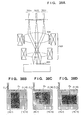
- Figs. 38B to 38D show a state in which the electron beams from the electron guns 501a, 501b, and 501c expose the corresponding exposure areas in exposure patterns to be formed in accordance with the same array. While setting and shifting the positions on the array in the order of (1,1), (1,2),..., (1,16), (2,1), (2,2),..., (2,16), (3,1), each electron beam is turned on at a position where an exposure pattern (P1, P2, P3) to be formed is present to expose the corresponding exposure area in the exposure pattern (P1, P2, P3) to be formed (i.e., so-called raster scan is performed).
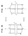
- the present invention provides an electron beam exposure apparatus having a source for emitting electron beams and a reduction electron optical system for reducing and projecting, on a target exposure surface, an image formed with the electron beam emitted from the source, comprising: a correction electron optical system arranged between the source and the reduction electron optical system to form a plurality of intermediate images of the source for correcting an aberration generated by the reduction electron optical system, the intermediate images being reduced and projected on the target exposure surface by the reduction electron optical system.
- the present invention provides an electron beam exposure method in which exposure is performed by making a source emit an electron beam to form an image, and reducing and projecting the image on a target exposure surface by a reduction electron optical system, comprising: the intermediate image formation step of forming a plurality of intermediate images of the source for correcting an aberration generated by the reduction electron optical system by a correction electron optical system arranged between the source and the reduction electron optical system.
- reference numeral 1 denotes an electron gun consisting of a cathode 1a, a grid 1b, and an anode 1c. Electrons emitted from the electron gun 1 form crossover image between the grid 1b and the anode 1c.
- crossover image Since an electron optical system (not shown) for enlarging/reducing or shaping the crossover image is used, enlarged/reduced or shaped crossover image can be obtained. With this arrangement, the size and shape of the crossover image can be changed (the crossover image will be referred to as a source hereinafter).
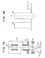
- the electron beam which is nearly collimated by the condenser lens 2 is formed into an intermediate image (MI) of the source on the blanking aperture 304 by the unipotential lens 303 through the blanking electrode 301 and the aperture (AP). If, at this time, no electric field is applied between the electrodes of the blanking electrode 301, an electron beam 305 is transmitted through the aperture of the blanking aperture 304. On the other hand, when an electric field is applied between the electrodes of the blanking electrode 301, an electron beam 306 is shielded by the blanking aperture 304.
- Fig. 6B shows another example of the element electron optical system which uses two lens arrays shown in Fig. 6A.
- Each element electron optical system is constituted by two unipotential lenses arranged at a predetermined interval. With this arrangement, the focal length and principal plane position of each element electron optical system can be independently controlled.
- the synthesized focal length and principal plane position of each element electron optical system can be independently set within limited ranges.
- the focal position (intermediate image formation position) changes by a distance corresponding to the moving amount of the major principal plane, as a matter of course.
- the focal lengths of the element electron optical systems can be made almost equal, and just the focal positions can be changed.
- the intermediate images of the source can be formed by the element electron optical systems at the same magnification (finally, the source images I1 and 12 on the wafer 5 are formed at the same magnification) while changing just the positions of the intermediate images along the optical axis.
- the sequence controller 14 controls a blanking control circuit 16 to turn on the blanking electrodes except that of the element electron optical system 31 (blanking on) such that only the electron beam from the element electron optical system 31 is irradiated on the X-Y-Z stage 11 side.
- the X-Y-Z stage 11 is driven by the stage drive control unit 23 to move the Faraday cup 10 close to the source image formed by the electron beam from the element electron optical system 31.
- the position of the X-Y-Z stage 11 at this time is detected by the laser interferometer 20.
- the sequence controller 14 While detecting the position of the X-Y-Z stage 11 and moving the X-Y-Z stage, the source image formed by the electron beam from the element electron optical system 32 is detected by the Faraday cup 10, thereby detecting the position and size of the source image and the irradiated current. In this way, the sequence controller 14 detects a position (X2,Y2,Z2) where the source image has a predetermined size and a current 12 irradiated at that time.
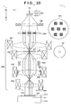
- reference numeral 601 denotes an electron gun consisting of a cathode 601a, a grid 601b, and an anode 601c. Electrons emitted from the cathode 601a form crossover image between the grid 601b and the anode 601c (the crossover image will be referred to as source hereinafter).
- the elements of the element electron optical system array 603 are set such that the interval between the sources on the wafer 605 becomes an integer multiple of the size of source image.
- the element electron optical system array 603 changes the positions of the intermediate images along the optical axis in accordance with the curvature of field of the reduction electron optical system 604, and at the same time, corrects in advance any aberration generated when each intermediate image is reduced and projected on the wafer 605 by the reduction electron optical system 604, as in the first mode of carrying out the invention.
- a deflector 606 deflects the plurality of electron beams from the element electron optical system array 603 to displace the plurality of source images in the X and Y directions on the wafer 605 by roughly the same amounts.
- the deflector 606 is constituted by a main deflector used when the deflection width is large, and a subdeflector used when the deflection width is small (neither are shown).
- the main deflector is an electromagnetic deflector
- the subdeflector is an electrostatic deflector.
- a ⁇ -Z stage 611 with a wafer mounted is movable along the optical axis AX (Z-axis) and in a rotational direction about the Z-axis.
- a stage reference plate 613 and the Faraday cup 610 are fixed on the ⁇ -Z stage 611.
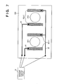
- Fig. 25 is a sectional view of each element electron optical system.
- reference numeral 701 denotes a blanking electrode consisting of a pair of electrodes and having a deflection function; and 702, a substrate common to the remaining element electron optical systems and having an aperture (AP) for defining the shape of the transmitted electron beam.
- a wiring layer (W) for turning on/off the blanking electrode 701 is formed on the substrate 702.
- Reference numeral 703 denotes an electron lens using two unipotential lenses 703a and 703b each consisting of three aperture electrodes and having a converging function for setting the upper and lower electrodes at an acceleration potential V0 and the intermediate electrode at another potential V1 or V2.
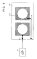
- Upper, intermediate, and lower electrodes 750 to 752 of the unipotential lens 703a and upper and lower electrodes 753 and 755 of the unipotential lens 703b have a shape shown in Fig. 26A.
- the upper and lower electrodes of the unipotential lenses 703a and 703b are set at a common potential by a first focus/astigmatism control circuit 615.
- An intermediate electrode 754 of the unipotential lens 703b is constituted by four electrodes as shown in Fig. 26B.
- the potentials of electrodes 703M can be independently set by the first focus/astigmatism control circuit 615.
- the potentials of the electrodes 703M are also independently set for each element electron optical system. Therefore, the focal length of the unipotential lens 703b can be changed along sections perpendicular to each other.
- the focal length of the unipotential lens 703b can be independently set for each element electron optical system. With this arrangement, the astigmatisms of the element electron optical systems can be independently controlled.
- the electron beam formed into an almost collimated beam by the condenser lens 602 passes through the blanking electrode 701 and the aperture (AP) and forms an intermediate image of the source through the electron lens 703. If, at this time, no electric field is applied between the electrodes of the blanking electrode 701, an electron beam 705 is not deflected. On the other hand, when an electric field is applied between the electrodes of the blanking electrode 701, an electron beam 706 is deflected. Since the electron beams 705 and 706 have different angular distributions on the object plane of the reduction electron optical system 604, the electron beams 705 and 706 are incident on different areas at the pupil position (on a plane P in Fig. 23) of the reduction electron optical system 604. Therefore, a blanking aperture BA for passing only the electron beam 705 is formed at the pupil position (on the plane P in Fig. 23) of the reduction electron optical system.
- the potentials of the two intermediate electrodes of each element electron optical system are independently set to change the electron optical characteristics (intermediate image formation position and astigmatism) of the element electron optical system.
- element electron optical systems in the same subarray are set to have the same electron optical characteristics so that the electron optical characteristics (intermediate image formation positions and astigmatisms) of the element electron optical systems are controlled in units of subarrays.
- the distortion characteristic of the reduction electron optical system 604 is determined in advance, and the position of each element electron optical system along the direction perpendicular to the optical axis of the reduction electron optical system 604 is set on the basis of the distortion characteristic.
- a blanking control circuit 614 independently controls ON/OFF of the blanking electrode of each element electron optical system of the element electron optical system array 603.
- the first focus/astigmatism control circuit 615 independently controls the electron optical characteristics (intermediate image formation position and astigmatism) of each element electron optical system of the element electron optical system array 603.
- a stage drive control circuit 620 drives and controls the ⁇ -Z stage 611 and also drives and controls the X-Y stage 612 in cooperation with a laser interferometer 621 for detecting the position of the X-Y stage 612.
- a control system 622 controls the above-described plurality of control circuits, the reflected electron detector 609, and the Faraday cup 610 in synchronism with each other for exposure and alignment based on data from a memory 623 which stores information associated with a drawing pattern.
- the control system 622 is controlled by a CPU 625 which controls the overall operation of the electron beam exposure apparatus through an interface 624.
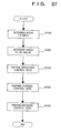
- the contour portion of the pattern must be precisely exposed. However, a portion except the contour portion of the pattern, i.e., inner portion of the pattern need not be precisely exposed, and a defined exposure amount need only be satisfied. This operation will be described with reference to Fig. 37.
- the CPU 625 determines an area F (black portion) on an array consisting of array positions (array elements FME) at which the contour portion is exposed, an area R (hatched portion) on an array consisting of array positions (array elements FME) at which the inner portion of the pattern is exposed, and an area N (white portion) on an array consisting of array positions (array elements FME) at which exposure is not performed, as shown in Figs. 29A and 29B.
- the contour portion may be regarded as an inner portion depending on the shape of the pattern.
- the width of the contour portion corresponds to one array element FME.
- the width of the contour portion may be represented by two array elements FME.
- the CPU 625 determines a first area FF (black portion) consisting of array positions at which the contour portion is exposed by at least one of the element electron optical systems a and b, a second area RR (hatched portion) different from the first area and consisting of array positions at which the inner portion of the pattern is exposed by at least one of the element electron optical systems a and b, and a third area NN (white portion) consisting of array positions at which neither of the element electron optical systems a and b perform exposure, as shown in Fig. 30A.
- the CPU 625 also divides the second area RR by an array element RME larger than the array interval of the array. At this time, an area which cannot be divided by the array element RME is added to the first area FF. The result is shown in Fig. 30B.
- the electron beams are deflected by the deflector 606 using the minimum deflection amount (array interval of the array) as a unit to perform exposure. With this operation, the contour portions of all exposure patterns to be formed on the wafer can be precisely reproduced.
- the electron beams are positioned in the second area RR on the array, the electron beams are deflected by the deflector 606 using a deflection amount larger than the minimum deflection amount (array interval of the array) as a unit to perform exposure. With this operation, the inner portion of the pattern which does not need high precision can be formed with a smaller number of times of exposure operations.
- the plurality of electron beams are positioned in the third area NN on the array, the positions of the electron beams are deflected without being set. With this operation, exposure can be performed while minimizing wasteful deflection of electron beams.
- the second area RR is divided only by the array element RME larger than the array interval of the array elements FME on the array.
- an area constituted by the array elements RME may be divided by an array element XRME larger than the array element RME.
- an area which cannot be divided by the array element XRME may be constituted by the array elements RME.
- Fig. 31C Deflection control data representing only the array elements FME, RME, and XRME to be exposed with the electron beams may be prepared.
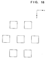
- Figs. 32A and 32B are views showing irradiation of electron beams from the element electron optical systems in correspondence with the array positions. More specifically, the electron beam is irradiated on a hatched array element.
- the CPU 625 prepares blanking control data corresponding to the array positions of each element electron optical system.
- the CPU 625 From data of the exposure pattern to be formed on the wafer, as shown in Fig. 33, the CPU 625 prepares exposure control data including the array positions, the types of array elements, the blanking control data including the operation time of the blanking electrode of each element electron optical system.
- the CPU 625 of the electron beam exposure apparatus performs the above processing. However, even when the processing is performed by an external processing unit, and the exposure control data is transferred to the CPU 625, the object and effect do not change.
- the control system 622 directs the deflection control circuit 617, on the basis of the exposure control data from the memory 623, which is transferred in synchronism with the internal reference clock, to cause the subdeflector of the deflector 606 to deflect the plurality of electron beams from the element electron optical system array 603, and also directs the blanking control circuit 614 to turn on/off the blanking electrodes of the element electron optical systems in accordance with the exposure pattern to be formed on the wafer 605.
- the deflection control circuit 617 controls the deflection position of the electron beam in consideration of the moving amount of the X-Y stage 612.
- the control system 622 changes the OFF time of the blanking electrode of each element electron optical system or changes the size of the source image on the wafer depending on the type of array element (FME, RME). Since the array element RME substantially has an exposure area larger than that of the array element FME, underexposure occurs if the same exposure time is set for the array elements FME and RME.
- the blanking electrode is controlled by the blanking control circuit 614 to prolong the exposure time for the array element RME.
- the size of crossover image of the sources of the electron gun 601 may be increased by an electron gun control circuit 631.
- the sequential control data may be changed to sequentially perform exposure first at deflection positions of the array elements RME, as shown in Fig. 34A, and next at deflection positions of the array elements FME, as shown in Fig. 34B.
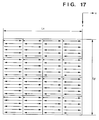
- the control system 622 After exposure of subfield 1 ⁇ shown in Fig. 19, the control system 622 directs the deflection control circuit 617 to make the main deflector of the deflector 606 deflect the plurality of electron beams from the element electron optical system array so as to expose subfield 2 ⁇ .
- the control system 622 commands the second focus/astigmatism control circuit 616 to control the dynamic focus coil 607 on the basis of dynamic focus correction data which has been obtained in advance, thereby correcting the focal position of the reduction electron optical system 604.
- the control system 622 commands control of the dynamic stigmatic coil 608 on the basis of dynamic astigmatism correction data which has been obtained in advance, thereby correcting the astigmatism of the reduction electron optical system.
- the operation of step 1 is performed to expose subfield 2 ⁇ .
- the size of the exposure pattern to be formed becomes small, a decrease in throughput can be minimized.
- This embodiment provides another operation of the electron beam exposure apparatus according to the first embodiment. Therefore, an electron beam exposure apparatus according to the second embodiment has the same arrangement as that of the electron beam exposure apparatus described in [Description of Constituent Elements of Electron Beam Exposure Apparatus] of the first embodiment.
- the control system 622 directs the first focus/astigmatism control circuit 615 to change setting of the intermediate image formation position of the element electron optical system of the subarray A (change the dynamic focus correction data for each subarray), scans the mark M(1,1) with the electron beam BE again, and obtains the blur of the beam in a similar manner.
- the control system 622 obtains dynamic focus correction data for the subarray A, which minimizes the blurs of the beam.
- the optimum dynamic focus correction data for the subarray A at the deflection position corresponding to the mark M(1,1) is determined. The above operation is performed for all marks, thereby determining optimum dynamic focus correction data for the subarray A at deflection positions corresponding to the respective marks.
- the control system 622 After exposure of subfield 1 ⁇ shown in Fig. 19, the control system 622 directs the deflection control circuit 617 to make the main deflector of the deflector 606 deflect the plurality of electron beams from the element electron optical system array so as to expose subfield 2 ⁇ . At this time, the control system 622 directs the second focus/astigmatism control circuit 616 to control the dynamic focus coil 607 on the basis of the above-described dynamic focus correction data, thereby correcting the focal position of the reduction electron optical system 604. At the same time, the control system 622 directs to control the dynamic stigmatic coil 608 on the basis of the above-described dynamic astigmatism correction data, thereby correcting the astigmatism of the reduction electron optical system.
- control system 622 commands the first focus/astigmatism control circuit 615 to control the electron optical characteristics (intermediate image formation positions and astigmatisms) of the element electron optical systems on the basis of the dynamic focus correction data and dynamic astigmatism correction data for each subarray.
- the operation in step 1 is performed to expose subfield 2 ⁇ .
- the control system 622 directs a blanking control circuit 614 to turn off only the blanking electrode of the element electron optical system A(3,3) while keeping the remaining blanking electrodes ON so that only the electron beam from the element electron optical system A(3,3) becomes incident on the wafer side.
- the control system 622 directs a deflection control circuit 617 to make the main deflector of a deflector 606 deflect an electron beam BE from the element electron optical system A(3,3) to the position of a mark M(1,1).
- the mark M(1,1) is scanned in the X direction. Reflected electrons/secondary electrons from the mark are detected by a reflected electron detector 609 and input to the control system 622.
- the control system 622 obtains the deviation between the actual deflection position and the designed deflection position in the X direction on the basis of the mark data.
- the control system 622 directs the deflection control circuit 617 to make the main deflector of the deflector 606 deflect the plurality of electron beams from the element electron optical system array so as to expose subfield 2 ⁇ .
- the control system 622 directs the subarray deflection control circuit 651 to control the deflector 650 corresponding to the subarray on the basis of the above-described dynamic deflection correction data for each subarray, thereby correcting the position of each intermediate image along the direction (X and Y directions) perpendicular to the optical axis.
- an electron beam exposure apparatus which can optimally correct deflection errors generated in the plurality of electron beams passing through the reduction electron optical system when the deflector is actuated in units of electron beams can be provided.
Landscapes
- Chemical & Material Sciences (AREA)
- Engineering & Computer Science (AREA)
- Nanotechnology (AREA)
- Analytical Chemistry (AREA)
- Crystallography & Structural Chemistry (AREA)
- Physics & Mathematics (AREA)
- Theoretical Computer Science (AREA)
- Mathematical Physics (AREA)
- Condensed Matter Physics & Semiconductors (AREA)
- General Physics & Mathematics (AREA)
- Manufacturing & Machinery (AREA)
- Electron Beam Exposure (AREA)
- Exposure And Positioning Against Photoresist Photosensitive Materials (AREA)
Applications Claiming Priority (9)
| Application Number | Priority Date | Filing Date | Title |
|---|---|---|---|
| JP04587896A JP3647128B2 (ja) | 1996-03-04 | 1996-03-04 | 電子ビーム露光装置とその露光方法 |
| JP4587896 | 1996-03-04 | ||
| JP10123396 | 1996-04-23 | ||
| JP10123396A JP3647136B2 (ja) | 1996-04-23 | 1996-04-23 | 電子ビーム露光装置 |
| JP15099096A JP3647143B2 (ja) | 1996-06-12 | 1996-06-12 | 電子ビーム露光装置及びその露光方法 |
| JP8150988A JPH09330868A (ja) | 1996-06-12 | 1996-06-12 | 電子ビーム露光方法及びそれを用いたデバイス製造方法 |
| JP15098896 | 1996-06-12 | ||
| JP15099096 | 1996-06-12 | ||
| EP97301406A EP0794552B1 (fr) | 1996-03-04 | 1997-03-04 | Appareil pour exposition par faisceau d'électrons, méthode d'exposition et procédé pour fabriquer un objet |
Related Parent Applications (1)
| Application Number | Title | Priority Date | Filing Date |
|---|---|---|---|
| EP97301406A Division EP0794552B1 (fr) | 1996-03-04 | 1997-03-04 | Appareil pour exposition par faisceau d'électrons, méthode d'exposition et procédé pour fabriquer un objet |
Publications (2)
| Publication Number | Publication Date |
|---|---|
| EP1369897A2 true EP1369897A2 (fr) | 2003-12-10 |
| EP1369897A3 EP1369897A3 (fr) | 2005-01-19 |
Family
ID=27461793
Family Applications (4)
| Application Number | Title | Priority Date | Filing Date |
|---|---|---|---|
| EP03077052A Withdrawn EP1369896A3 (fr) | 1996-03-04 | 1997-03-04 | Appareil d'exposition à faisceau d'électrons et procédé et dispositif de fabrication |
| EP03077053A Withdrawn EP1369897A3 (fr) | 1996-03-04 | 1997-03-04 | Appareil d'exposition à faisceau d'électrons et procédé et dispositif de fabrication |
| EP97301406A Expired - Lifetime EP0794552B1 (fr) | 1996-03-04 | 1997-03-04 | Appareil pour exposition par faisceau d'électrons, méthode d'exposition et procédé pour fabriquer un objet |
| EP03077051A Expired - Lifetime EP1369895B1 (fr) | 1996-03-04 | 1997-03-04 | Appareil d'exposition à faisceau d'électrons et procédé et dispositif de fabrication |
Family Applications Before (1)
| Application Number | Title | Priority Date | Filing Date |
|---|---|---|---|
| EP03077052A Withdrawn EP1369896A3 (fr) | 1996-03-04 | 1997-03-04 | Appareil d'exposition à faisceau d'électrons et procédé et dispositif de fabrication |
Family Applications After (2)
| Application Number | Title | Priority Date | Filing Date |
|---|---|---|---|
| EP97301406A Expired - Lifetime EP0794552B1 (fr) | 1996-03-04 | 1997-03-04 | Appareil pour exposition par faisceau d'électrons, méthode d'exposition et procédé pour fabriquer un objet |
| EP03077051A Expired - Lifetime EP1369895B1 (fr) | 1996-03-04 | 1997-03-04 | Appareil d'exposition à faisceau d'électrons et procédé et dispositif de fabrication |
Country Status (4)
| Country | Link |
|---|---|
| US (4) | US5834783A (fr) |
| EP (4) | EP1369896A3 (fr) |
| KR (1) | KR100225335B1 (fr) |
| DE (1) | DE69738276T2 (fr) |
Cited By (1)
| Publication number | Priority date | Publication date | Assignee | Title |
|---|---|---|---|---|
| US7173262B2 (en) | 2004-06-30 | 2007-02-06 | Canon Kabushiki Kaisha | Charged particle beam exposure apparatus, charged particle beam exposure method and device manufacturing method |
Families Citing this family (163)
| Publication number | Priority date | Publication date | Assignee | Title |
|---|---|---|---|---|
| JPH10144583A (ja) * | 1996-11-07 | 1998-05-29 | Nikon Corp | 荷電粒子線投影方法および荷電粒子線投影装置 |
| US5981954A (en) * | 1997-01-16 | 1999-11-09 | Canon Kabushiki Kaisha | Electron beam exposure apparatus |
| US6107636A (en) | 1997-02-07 | 2000-08-22 | Canon Kabushiki Kaisha | Electron beam exposure apparatus and its control method |
| KR19980079377A (ko) * | 1997-03-25 | 1998-11-25 | 요시다쇼이치로 | 하전립자선 전사장치 |
| US6274877B1 (en) | 1997-05-08 | 2001-08-14 | Canon Kabushiki Kaisha | Electron beam exposure apparatus |
| US6104035A (en) * | 1997-06-02 | 2000-08-15 | Canon Kabushiki Kaisha | Electron-beam exposure apparatus and method |
| JP4207232B2 (ja) * | 1997-09-02 | 2009-01-14 | 株式会社ニコン | 荷電ビーム露光装置 |
| US6175122B1 (en) * | 1998-01-09 | 2001-01-16 | International Business Machines Corporation | Method for writing a pattern using multiple variable shaped electron beams |
| US5981962A (en) * | 1998-01-09 | 1999-11-09 | International Business Machines Corporation | Distributed direct write lithography system using multiple variable shaped electron beams |
| US6674086B2 (en) * | 1998-03-20 | 2004-01-06 | Hitachi, Ltd. | Electron beam lithography system, electron beam lithography apparatus, and method of lithography |
| US6124140A (en) * | 1998-05-22 | 2000-09-26 | Micron Technology, Inc. | Method for measuring features of a semiconductor device |
| US6218676B1 (en) | 1998-06-05 | 2001-04-17 | Nikon Corporation | Charged-particle-beam image-transfer apparatus exhibiting reduced space-charge effects and device fabrication methods using the same |
| JP3982913B2 (ja) * | 1998-07-17 | 2007-09-26 | 株式会社アドバンテスト | 荷電粒子ビーム露光装置 |
| US6360134B1 (en) | 1998-07-20 | 2002-03-19 | Photronics, Inc. | Method for creating and improved image on a photomask by negatively and positively overscanning the boundaries of an image pattern at inside corner locations |
| JP3825921B2 (ja) * | 1998-07-23 | 2006-09-27 | キヤノン株式会社 | 走査露光装置およびデバイス製造方法 |
| JP3241011B2 (ja) * | 1998-11-20 | 2001-12-25 | 日本電気株式会社 | 電子線露光装置及び電子線露光用マスク |
| JP4410871B2 (ja) * | 1999-03-25 | 2010-02-03 | キヤノン株式会社 | 荷電粒子線露光装置及び該装置を用いたデバイス製造方法 |
| US6630681B1 (en) * | 1999-07-21 | 2003-10-07 | Nikon Corporation | Charged-particle-beam microlithography apparatus and methods including correction of aberrations caused by space-charge effects |
| US6472673B1 (en) * | 1999-07-29 | 2002-10-29 | Ims Ionen-Mikrofabrikations Systeme Gmbh | Lithographic method for producing an exposure pattern on a substrate |
| JP2001076990A (ja) | 1999-08-31 | 2001-03-23 | Canon Inc | 荷電粒子線露光装置及びその制御方法 |
| US6635891B1 (en) | 1999-09-22 | 2003-10-21 | Nikon Corporation | Hollow-beam apertures for charged-particle-beam microlithography apparatus and methods for making and using same |
| JP3763446B2 (ja) | 1999-10-18 | 2006-04-05 | キヤノン株式会社 | 静電レンズ、電子ビーム描画装置、荷電ビーム応用装置、および、デバイス製造方法 |
| JP2001168016A (ja) | 1999-12-13 | 2001-06-22 | Canon Inc | 荷電粒子線露光装置と露光システム及びそれらの制御方法及びデバイス製造方法 |
| JP2001168018A (ja) | 1999-12-13 | 2001-06-22 | Canon Inc | 荷電粒子線露光装置、荷電粒子線露光方法及び露光補正データの決定方法、該方法を適用したデバイスの製造方法。 |
| JP2001168017A (ja) | 1999-12-13 | 2001-06-22 | Canon Inc | 荷電粒子線露光装置、荷電粒子線露光方法及び制御データの決定方法、該方法を適用したデバイスの製造方法。 |
| US6566664B2 (en) | 2000-03-17 | 2003-05-20 | Canon Kabushiki Kaisha | Charged-particle beam exposure apparatus and device manufacturing method |
| JP2001284230A (ja) | 2000-03-31 | 2001-10-12 | Canon Inc | 電子光学系アレイ、これを用いた荷電粒子線露光装置ならびにデバイス製造方法 |
| JP2001283756A (ja) | 2000-03-31 | 2001-10-12 | Canon Inc | 電子光学系アレイ、これを用いた荷電粒子線露光装置ならびにデバイス製造方法 |
| JP4947842B2 (ja) | 2000-03-31 | 2012-06-06 | キヤノン株式会社 | 荷電粒子線露光装置 |
| JP4585661B2 (ja) | 2000-03-31 | 2010-11-24 | キヤノン株式会社 | 電子光学系アレイ、荷電粒子線露光装置およびデバイス製造方法 |
| JP4947841B2 (ja) | 2000-03-31 | 2012-06-06 | キヤノン株式会社 | 荷電粒子線露光装置 |
| US6787780B2 (en) * | 2000-04-04 | 2004-09-07 | Advantest Corporation | Multi-beam exposure apparatus using a multi-axis electron lens, fabrication method of a semiconductor device |
| US6291940B1 (en) * | 2000-06-09 | 2001-09-18 | Applied Materials, Inc. | Blanker array for a multipixel electron source |
| SG103303A1 (en) * | 2000-07-07 | 2004-04-29 | Nikon Corp | Exposure apparatus, surface position adjustment unit, mask, and device manufacturing method |
| US6433348B1 (en) * | 2000-07-25 | 2002-08-13 | Applied Materials, Inc. | Lithography using multiple pass raster-shaped beam |
| JP2002118060A (ja) * | 2000-07-27 | 2002-04-19 | Toshiba Corp | 荷電ビーム露光装置、荷電ビーム露光方法、露光データ作成方法、露光データを作成するプログラムを記録したコンピュータ読取り可能な記録媒体、及び、露光データを記録したコンピュータ読取り可能な記録媒体 |
| DE60134922D1 (de) * | 2000-08-14 | 2008-09-04 | Elith Llc | Lithographischer Apparat |
| EP1182684B1 (fr) * | 2000-08-14 | 2008-07-23 | eLith LLC | Appareil lithographique |
| US7085351B2 (en) * | 2000-10-06 | 2006-08-01 | University Of North Carolina At Chapel Hill | Method and apparatus for controlling electron beam current |
| US6876724B2 (en) * | 2000-10-06 | 2005-04-05 | The University Of North Carolina - Chapel Hill | Large-area individually addressable multi-beam x-ray system and method of forming same |
| JP4178741B2 (ja) * | 2000-11-02 | 2008-11-12 | 株式会社日立製作所 | 荷電粒子線装置および試料作製装置 |
| JP2002217088A (ja) * | 2001-01-17 | 2002-08-02 | Nikon Corp | 荷電粒子線露光装置、荷電粒子線露光方法及び半導体デバイスの製造方法 |
| US20020170887A1 (en) * | 2001-03-01 | 2002-11-21 | Konica Corporation | Optical element producing method, base material drawing method and base material drawing apparatus |
| DE10109965A1 (de) * | 2001-03-01 | 2002-09-12 | Zeiss Carl | Teilchenoptische Linsenanordnung und Verfahren unter Einsatz einer solchen Linsenanordnung |
| JP4647820B2 (ja) * | 2001-04-23 | 2011-03-09 | キヤノン株式会社 | 荷電粒子線描画装置、および、デバイスの製造方法 |
| JP2002343295A (ja) * | 2001-05-21 | 2002-11-29 | Canon Inc | 電子線露光装置、縮小投影系及びデバイス製造方法 |
| JP2003100591A (ja) * | 2001-09-21 | 2003-04-04 | Nikon Corp | 荷電粒子線露光装置における露光方法、半導体デバイスの製造方法及び荷電粒子線露光装置 |
| JP4822486B2 (ja) * | 2001-09-26 | 2011-11-24 | Nltテクノロジー株式会社 | 半透過反射板及び半透過型液晶表示装置 |
| DE10160917A1 (de) * | 2001-12-07 | 2003-06-26 | Kleo Halbleitertechnik Gmbh | Lithografiebelichtungseinrichtung |
| JP2003203836A (ja) | 2001-12-28 | 2003-07-18 | Canon Inc | 露光装置及びその制御方法並びにデバイス製造方法 |
| US6853143B2 (en) * | 2002-01-09 | 2005-02-08 | Ebara Corporation | Electron beam system and method of manufacturing devices using the system |
| US6639221B2 (en) | 2002-01-18 | 2003-10-28 | Nikon Corporation | Annular illumination method for charged particle projection optics |
| US6614035B2 (en) * | 2002-01-30 | 2003-09-02 | International Business Machines Corporation | Multi-beam shaped beam lithography system |
| JPWO2004006307A1 (ja) * | 2002-07-03 | 2005-11-10 | 株式会社ピー・ディー・サービス | 電子ビーム露光方法及びその装置 |
| JP2004055767A (ja) | 2002-07-18 | 2004-02-19 | Canon Inc | 電子ビーム露光装置及び半導体デバイスの製造方法 |
| JP4017935B2 (ja) * | 2002-07-30 | 2007-12-05 | 株式会社日立ハイテクノロジーズ | マルチビーム型電子線描画方法及び装置 |
| DE10237141A1 (de) * | 2002-08-13 | 2004-02-26 | Leo Elektronenmikroskopie Gmbh | Strahlführungssystem, Abbildungsverfahren und Elektronenmikroskopiesystem |
| JP3826087B2 (ja) * | 2002-08-30 | 2006-09-27 | キヤノン株式会社 | 位置決め装置、荷電粒子線露光装置 |
| EP2302457B1 (fr) | 2002-10-25 | 2016-03-30 | Mapper Lithography Ip B.V. | Système de lithographie |
| CN101414534B (zh) * | 2002-10-30 | 2012-10-03 | 迈普尔平版印刷Ip有限公司 | 电子束曝光系统 |
| US7098468B2 (en) * | 2002-11-07 | 2006-08-29 | Applied Materials, Inc. | Raster frame beam system for electron beam lithography |
| US6936981B2 (en) * | 2002-11-08 | 2005-08-30 | Applied Materials, Inc. | Retarding electron beams in multiple electron beam pattern generation |
| JP4167050B2 (ja) * | 2002-12-13 | 2008-10-15 | キヤノン株式会社 | 荷電粒子線露光装置及びその制御方法、並びにデバイス製造方法 |
| JP4167904B2 (ja) * | 2003-01-06 | 2008-10-22 | 株式会社日立ハイテクノロジーズ | 電子ビーム描画装置及び電子ビーム描画方法 |
| US7337903B2 (en) * | 2003-01-07 | 2008-03-04 | Lauri Aaron P | Single edge razor blade holder |
| EP1439566B1 (fr) | 2003-01-17 | 2019-08-28 | ICT, Integrated Circuit Testing Gesellschaft für Halbleiterprüftechnik mbH | Appareillage émettant un faisceau de particules chargés et sa méthode de commande |
| EP2267747B1 (fr) | 2003-02-14 | 2014-05-14 | Mapper Lithography Ip B.V. | Système de lithographie avec cathode à réserve |
| US7081369B2 (en) * | 2003-02-28 | 2006-07-25 | Intel Corporation | Forming a semiconductor device feature using acquired parameters |
| KR101068607B1 (ko) | 2003-03-10 | 2011-09-30 | 마퍼 리쏘그라피 아이피 비.브이. | 복수 개의 빔렛 발생 장치 |
| JP4421836B2 (ja) * | 2003-03-28 | 2010-02-24 | キヤノン株式会社 | 露光装置及びデバイス製造方法 |
| US7005659B2 (en) * | 2003-07-08 | 2006-02-28 | Canon Kabushiki Kaisha | Charged particle beam exposure apparatus, charged particle beam exposure method, and device manufacturing method using the same apparatus |
| JP2005032837A (ja) * | 2003-07-08 | 2005-02-03 | Canon Inc | 荷電粒子描画方法及び該方法を用いたデバイス製造方法 |
| JP4738723B2 (ja) * | 2003-08-06 | 2011-08-03 | キヤノン株式会社 | マルチ荷電粒子線描画装置、荷電粒子線の電流の測定方法及びデバイス製造方法 |
| CN102709143B (zh) * | 2003-09-05 | 2016-03-09 | 卡尔蔡司Smt有限责任公司 | 电子光学排布结构、多电子分束检验系统和方法 |
| JP2005129850A (ja) * | 2003-10-27 | 2005-05-19 | Toshiba Corp | 荷電ビーム描画装置及び描画方法 |
| GB2408383B (en) * | 2003-10-28 | 2006-05-10 | Ims Nanofabrication Gmbh | Pattern-definition device for maskless particle-beam exposure apparatus |
| DE10352040A1 (de) * | 2003-11-07 | 2005-07-21 | Carl Zeiss Sms Gmbh | In Lage, Form und/oder den optischen Eigenschaften veränderbare Blenden-und/oder Filteranordnung für optische Geräte, insbesondere Mikroskope |
| GB2412232A (en) * | 2004-03-15 | 2005-09-21 | Ims Nanofabrication Gmbh | Particle-optical projection system |
| JP2005268268A (ja) * | 2004-03-16 | 2005-09-29 | Canon Inc | 電子ビーム露光装置 |
| EP1577926A1 (fr) * | 2004-03-19 | 2005-09-21 | ICT, Integrated Circuit Testing Gesellschaft für Halbleiterprüftechnik Mbh | Système à faisceau de particules à haute densité de courant |
| KR100722672B1 (ko) * | 2004-12-27 | 2007-05-28 | 동부일렉트로닉스 주식회사 | 렌즈의 축소율 조절이 가능한 노광 장비 |
| JP4652830B2 (ja) * | 2005-01-26 | 2011-03-16 | キヤノン株式会社 | 収差調整方法、デバイス製造方法及び荷電粒子線露光装置 |
| US7468506B2 (en) * | 2005-01-26 | 2008-12-23 | Applied Materials, Israel, Ltd. | Spot grid array scanning system |
| US7468507B2 (en) * | 2005-01-26 | 2008-12-23 | Applied Materials, Israel, Ltd. | Optical spot grid array scanning system |
| JP4657740B2 (ja) * | 2005-01-26 | 2011-03-23 | キヤノン株式会社 | 荷電粒子線光学系用収差測定装置、該収差測定装置を具備する荷電粒子線露光装置及び該装置を用いたデバイス製造方法 |
| US7403265B2 (en) | 2005-03-30 | 2008-07-22 | Asml Netherlands B.V. | Lithographic apparatus and device manufacturing method utilizing data filtering |
| US8155262B2 (en) | 2005-04-25 | 2012-04-10 | The University Of North Carolina At Chapel Hill | Methods, systems, and computer program products for multiplexing computed tomography |
| JP4708854B2 (ja) * | 2005-05-13 | 2011-06-22 | 株式会社日立ハイテクノロジーズ | 荷電粒子線装置 |
| US7781748B2 (en) | 2006-04-03 | 2010-08-24 | Ims Nanofabrication Ag | Particle-beam exposure apparatus with overall-modulation of a patterned beam |
| US8189893B2 (en) | 2006-05-19 | 2012-05-29 | The University Of North Carolina At Chapel Hill | Methods, systems, and computer program products for binary multiplexing x-ray radiography |
| JP2008004596A (ja) * | 2006-06-20 | 2008-01-10 | Canon Inc | 荷電粒子線描画方法、露光装置、及びデバイス製造方法 |
| US8049865B2 (en) | 2006-09-18 | 2011-11-01 | Asml Netherlands B.V. | Lithographic system, device manufacturing method, and mask optimization method |
| US8129190B2 (en) * | 2006-11-17 | 2012-03-06 | Applied Nanotech Holdings, Inc. | Tagged petroleum products and methods of detecting same |
| WO2008117358A1 (fr) * | 2007-03-22 | 2008-10-02 | Pioneer Corporation | Dispositif de faisceau électronique |
| WO2009012453A1 (fr) * | 2007-07-19 | 2009-01-22 | The University Of North Carolina At Chapel Hill | Systèmes de tomosynthèse numérique du sein aux rayons x stationnaires et procédés apparentés |
| US8642959B2 (en) * | 2007-10-29 | 2014-02-04 | Micron Technology, Inc. | Method and system of performing three-dimensional imaging using an electron microscope |
| JP2010067399A (ja) * | 2008-09-09 | 2010-03-25 | Canon Inc | 導電性部材の製造方法、及びこれを用いた電子源の製造方法 |
| JP5277250B2 (ja) * | 2008-09-25 | 2013-08-28 | 株式会社日立ハイテクノロジーズ | 荷電粒子線応用装置およびその幾何収差測定方法 |
| DE102008062450B4 (de) * | 2008-12-13 | 2012-05-03 | Vistec Electron Beam Gmbh | Anordnung zur Beleuchtung eines Substrats mit mehreren individuell geformten Partikelstrahlen zur hochauflösenden Lithographie von Strukturmustern |
| JP5634052B2 (ja) * | 2009-01-09 | 2014-12-03 | キヤノン株式会社 | 荷電粒子線描画装置およびデバイス製造方法 |
| US8600003B2 (en) | 2009-01-16 | 2013-12-03 | The University Of North Carolina At Chapel Hill | Compact microbeam radiation therapy systems and methods for cancer treatment and research |
| US8294125B2 (en) * | 2009-11-18 | 2012-10-23 | Kla-Tencor Corporation | High-sensitivity and high-throughput electron beam inspection column enabled by adjustable beam-limiting aperture |
| US8358739B2 (en) | 2010-09-03 | 2013-01-22 | The University Of North Carolina At Chapel Hill | Systems and methods for temporal multiplexing X-ray imaging |
| JP5606292B2 (ja) | 2010-11-19 | 2014-10-15 | キヤノン株式会社 | 描画装置、物品の製造方法、偏向装置の製造方法、および、描画装置の製造方法 |
| JP5809419B2 (ja) * | 2011-02-18 | 2015-11-10 | 株式会社ニューフレアテクノロジー | 荷電粒子ビーム描画装置及び荷電粒子ビーム描画方法 |
| NL2006868C2 (en) | 2011-05-30 | 2012-12-03 | Mapper Lithography Ip Bv | Charged particle multi-beamlet apparatus. |
| JP2013045838A (ja) * | 2011-08-23 | 2013-03-04 | Canon Inc | 描画装置、および、物品の製造方法 |
| JP5707286B2 (ja) * | 2011-09-21 | 2015-04-30 | 株式会社日立ハイテクノロジーズ | 荷電粒子線装置、荷電粒子線装置の調整方法、および試料の検査若しくは試料の観察方法。 |
| EP2750165B1 (fr) | 2011-10-03 | 2016-07-13 | Param Corporation | Procédé lithographique par faisceaus d'électrons |
| JP2013172106A (ja) * | 2012-02-22 | 2013-09-02 | Canon Inc | 描画装置及び物品の製造方法 |
| US10586625B2 (en) | 2012-05-14 | 2020-03-10 | Asml Netherlands B.V. | Vacuum chamber arrangement for charged particle beam generator |
| JP2013255974A (ja) * | 2012-06-14 | 2013-12-26 | Canon Inc | マイクロ構造体及びその製造方法 |
| JP6080540B2 (ja) * | 2012-12-26 | 2017-02-15 | 株式会社ニューフレアテクノロジー | 荷電粒子ビーム描画装置 |
| JP2014220263A (ja) * | 2013-04-30 | 2014-11-20 | キヤノン株式会社 | リソグラフィ装置、及び物品の製造方法 |
| JP6230295B2 (ja) * | 2013-06-26 | 2017-11-15 | キヤノン株式会社 | 描画装置及び物品の製造方法 |
| NL2013814B1 (en) * | 2013-11-14 | 2016-05-10 | Mapper Lithography Ip Bv | Multi-electrode vacuum arrangement. |
| JP6190254B2 (ja) | 2013-12-04 | 2017-08-30 | 株式会社ニューフレアテクノロジー | マルチ荷電粒子ビーム描画装置及びマルチ荷電粒子ビーム描画方法 |
| JP6353229B2 (ja) * | 2014-01-22 | 2018-07-04 | 株式会社ニューフレアテクノロジー | マルチ荷電粒子ビーム描画装置及びマルチ荷電粒子ビーム描画方法 |
| US9782136B2 (en) | 2014-06-17 | 2017-10-10 | The University Of North Carolina At Chapel Hill | Intraoral tomosynthesis systems, methods, and computer readable media for dental imaging |
| US10980494B2 (en) | 2014-10-20 | 2021-04-20 | The University Of North Carolina At Chapel Hill | Systems and related methods for stationary digital chest tomosynthesis (s-DCT) imaging |
| JP5816739B1 (ja) * | 2014-12-02 | 2015-11-18 | 株式会社ニューフレアテクノロジー | マルチビームのブランキングアパーチャアレイ装置、及びマルチビームのブランキングアパーチャアレイ装置の製造方法 |
| JP2016122676A (ja) * | 2014-12-24 | 2016-07-07 | 株式会社アドバンテスト | 露光装置および露光方法 |
| DE102015202172B4 (de) | 2015-02-06 | 2017-01-19 | Carl Zeiss Microscopy Gmbh | Teilchenstrahlsystem und Verfahren zur teilchenoptischen Untersuchung eines Objekts |
| JP6577787B2 (ja) | 2015-08-11 | 2019-09-18 | 株式会社ニューフレアテクノロジー | マルチ荷電粒子ビーム描画装置及びマルチ荷電粒子ビーム描画方法 |
| US9679742B2 (en) * | 2015-10-30 | 2017-06-13 | Fei Company | Method for optimizing charged particle beams formed by shaped apertures |
| US10497536B2 (en) * | 2016-09-08 | 2019-12-03 | Rockwell Collins, Inc. | Apparatus and method for correcting arrayed astigmatism in a multi-column scanning electron microscopy system |
| JP6700152B2 (ja) * | 2016-10-18 | 2020-05-27 | 株式会社ニューフレアテクノロジー | マルチビーム焦点調整方法およびマルチビーム焦点測定方法 |
| JP6791051B2 (ja) * | 2017-07-28 | 2020-11-25 | 株式会社ニューフレアテクノロジー | マルチ荷電粒子ビーム描画装置及びマルチ荷電粒子ビーム描画方法 |
| JP6854215B2 (ja) * | 2017-08-02 | 2021-04-07 | 株式会社ニューフレアテクノロジー | マルチ荷電粒子ビーム描画装置及びマルチ荷電粒子ビーム描画方法 |
| DE102018202428B3 (de) | 2018-02-16 | 2019-05-09 | Carl Zeiss Microscopy Gmbh | Vielstrahl-Teilchenmikroskop |
| DE102018202421B3 (de) | 2018-02-16 | 2019-07-11 | Carl Zeiss Microscopy Gmbh | Vielstrahl-Teilchenstrahlsystem |
| CN112055886A (zh) | 2018-02-27 | 2020-12-08 | 卡尔蔡司MultiSEM有限责任公司 | 带电粒子多束系统及方法 |
| US10811215B2 (en) | 2018-05-21 | 2020-10-20 | Carl Zeiss Multisem Gmbh | Charged particle beam system |
| DE102018115012A1 (de) | 2018-06-21 | 2019-12-24 | Carl Zeiss Microscopy Gmbh | Teilchenstrahlsystem |
| EP3624167A1 (fr) | 2018-09-14 | 2020-03-18 | FEI Company | Appareil d'imagerie à faisceaux d'électrons multiples et à performances améliorées |
| DE102018007455B4 (de) | 2018-09-21 | 2020-07-09 | Carl Zeiss Multisem Gmbh | Verfahren zum Detektorabgleich bei der Abbildung von Objekten mittels eines Mehrstrahl-Teilchenmikroskops, System sowie Computerprogrammprodukt |
| DE102018007652B4 (de) | 2018-09-27 | 2021-03-25 | Carl Zeiss Multisem Gmbh | Teilchenstrahl-System sowie Verfahren zur Stromregulierung von Einzel-Teilchenstrahlen |
| DE102018124044B3 (de) | 2018-09-28 | 2020-02-06 | Carl Zeiss Microscopy Gmbh | Verfahren zum Betreiben eines Vielstrahl-Teilchenstrahlmikroskops und Vielstrahl-Teilchenstrahlsystem |
| DE102018124219A1 (de) | 2018-10-01 | 2020-04-02 | Carl Zeiss Microscopy Gmbh | Vielstrahl-Teilchenstrahlsystem und Verfahren zum Betreiben eines solchen |
| US11145485B2 (en) * | 2018-12-26 | 2021-10-12 | Nuflare Technology, Inc. | Multiple electron beams irradiation apparatus |
| TWI743626B (zh) | 2019-01-24 | 2021-10-21 | 德商卡爾蔡司多重掃描電子顯微鏡有限公司 | 包含多束粒子顯微鏡的系統、對3d樣本逐層成像之方法及電腦程式產品 |
| CN111477530B (zh) | 2019-01-24 | 2023-05-05 | 卡尔蔡司MultiSEM有限责任公司 | 利用多束粒子显微镜对3d样本成像的方法 |
| CN110031887B (zh) * | 2019-04-30 | 2022-01-04 | 清华大学 | 电子束斑标定装置和方法 |
| DE102019004124B4 (de) | 2019-06-13 | 2024-03-21 | Carl Zeiss Multisem Gmbh | Teilchenstrahl-System zur azimutalen Ablenkung von Einzel-Teilchenstrahlen sowie seine Verwendung und Verfahren zur Azimut-Korrektur bei einem Teilchenstrahl-System |
| DE102019005362A1 (de) | 2019-07-31 | 2021-02-04 | Carl Zeiss Multisem Gmbh | Verfahren zum Betreiben eines Vielzahl-Teilchenstrahlsystems unter Veränderung der numerischen Apertur, zugehöriges Computerprogrammprodukt und Vielzahl-Teilchenstrahlsystem |
| WO2021071357A1 (fr) | 2019-10-08 | 2021-04-15 | Technische Universiteit Delft | Dispositif pour générer une pluralité de petits faisceaux de particules chargées, et appareil d'inspection, d'imagerie ou de traitement et son procédé d'utilisation |
| DE102019008249B3 (de) | 2019-11-27 | 2020-11-19 | Carl Zeiss Multisem Gmbh | Teilchenstrahl-System mit einer Multistrahl-Ablenkeinrichtung und einem Strahlfänger, Verfahren zum Betreiben des Teilchenstrahl-Systems und zugehöriges Computerprogrammprodukt |
| EP4100986A1 (fr) | 2020-02-04 | 2022-12-14 | Carl Zeiss MultiSEM GmbH | Balayage numérique à faisceaux multiples et acquisition d'image |
| JP7689139B2 (ja) | 2020-03-12 | 2025-06-05 | カール ツァイス マルティセム ゲゼルシヤフト ミット ベシュレンクテル ハフツング | マルチビーム発生ユニットおよびマルチビーム偏向ユニットの特定の改善 |
| DE102020107738B3 (de) | 2020-03-20 | 2021-01-14 | Carl Zeiss Multisem Gmbh | Teilchenstrahl-System mit einer Multipol-Linsen-Sequenz zur unabhängigen Fokussierung einer Vielzahl von Einzel-Teilchenstrahlen, seine Verwendung und zugehöriges Verfahren |
| EP3893263A1 (fr) * | 2020-04-06 | 2021-10-13 | ASML Netherlands B.V. | Ensemble d'ouverture, unité de manipulation de faisceau, procédé de manipulation de faisceaux de particules chargées et appareil de projection de particules chargées |
| JP7474151B2 (ja) * | 2020-08-21 | 2024-04-24 | 株式会社ニューフレアテクノロジー | マルチ電子ビーム描画装置及びマルチ電子ビーム描画方法 |
| DE102020123567B4 (de) | 2020-09-09 | 2025-02-13 | Carl Zeiss Multisem Gmbh | Vielzahl-Teilchenstrahl-System mit Kontrast-Korrektur-Linsen-System |
| TW202220012A (zh) | 2020-09-30 | 2022-05-16 | 德商卡爾蔡司多重掃描電子顯微鏡有限公司 | 在可調工作距離附近具快速自動對焦之多重粒子束顯微鏡及相關方法 |
| DE102021200799B3 (de) | 2021-01-29 | 2022-03-31 | Carl Zeiss Multisem Gmbh | Verfahren mit verbesserter Fokuseinstellung unter Berücksichtigung eines Bildebenenkipps in einem Vielzahl-Teilchenstrahlmikroskop |
| TW202312205A (zh) | 2021-05-27 | 2023-03-16 | 德商卡爾蔡司多重掃描電子顯微鏡有限公司 | 多重射束帶電粒子系統與在多重射束帶電粒子系統中控制工作距離的方法 |
| DE102021116969B3 (de) | 2021-07-01 | 2022-09-22 | Carl Zeiss Multisem Gmbh | Verfahren zur bereichsweisen Probeninspektion mittels eines Vielstrahl-Teilchenmikroskopes, Computerprogrammprodukt und Vielstrahl-Teilchenmikroskop zur Halbleiterprobeninspektion |
| CN114995073A (zh) * | 2022-07-08 | 2022-09-02 | 西湖大学 | 光电发射多束电子束曝光机 |
| US12567560B2 (en) * | 2022-09-28 | 2026-03-03 | Kla Corporation | Distortion reduction in a multi-beam imaging system |
| DE102022131862A1 (de) * | 2022-12-01 | 2024-06-06 | Carl Zeiss Multisem Gmbh | Vielstrahl-Teilchenmikroskop umfassend eine Aberrationskorrektureinheit mit Geometrie-basierten Korrekturelektroden und Verfahren zum Einstellen der Aberrationskorrektur sowie Computerprogrammprodukt |
| DE102023101774B4 (de) | 2023-01-25 | 2025-05-15 | Carl Zeiss Multisem Gmbh | Verfahren zum Auslegen eines Vielstrahl-Teilchenstrahlsystems mit monolithischen Bahnverlaufskorrekturplatten, Computerprogrammprodukt und Vielstrahl-Teilchenstrahlsystem |
| WO2024156469A1 (fr) | 2023-01-25 | 2024-08-02 | Carl Zeiss Multisem Gmbh | Microscope à particules à faisceaux multiples avec générateur à faisceaux multiples amélioré pour correction de courbure de champ et générateur à faisceaux multiples |
| DE102023120127B4 (de) | 2023-07-28 | 2025-03-27 | Carl Zeiss Multisem Gmbh | Teilchenoptische Anordnung, insbesondere Vielstrahl-Teilchenmikroskop, mit einer Magnetanordnung zum Separieren eines primären und eines sekundären teilchenoptischen Strahlenganges mit verbesserter Performance |
Family Cites Families (22)
| Publication number | Priority date | Publication date | Assignee | Title |
|---|---|---|---|---|
| JPS52119178A (en) * | 1976-03-31 | 1977-10-06 | Toshiba Corp | Electron beam exposure device |
| CA1100237A (fr) * | 1977-03-23 | 1981-04-28 | Roger F.W. Pease | Traduction non-disponible |
| US4158140A (en) * | 1977-06-15 | 1979-06-12 | Tokyo Shibaura Electric Co., Ltd. | Electron beam exposure apparatus |
| US4142132A (en) * | 1977-07-05 | 1979-02-27 | Control Data Corporation | Method and means for dynamic correction of electrostatic deflector for electron beam tube |
| FR2443085A1 (fr) * | 1978-07-24 | 1980-06-27 | Thomson Csf | Dispositif de microlithographie par bombardement electronique |
| US4200794A (en) * | 1978-11-08 | 1980-04-29 | Control Data Corporation | Micro lens array and micro deflector assembly for fly's eye electron beam tubes using silicon components and techniques of fabrication and assembly |
| US4472636A (en) * | 1979-11-01 | 1984-09-18 | Eberhard Hahn | Method of and device for corpuscular projection |
| US4338548A (en) * | 1980-01-30 | 1982-07-06 | Control Data Corporation | Unipotential lens assembly for charged particle beam tubes and method for applying correction potentials thereto |
| DE3169257D1 (en) * | 1980-11-28 | 1985-04-18 | Ibm | Electron beam system and method |
| US4498010A (en) * | 1983-05-05 | 1985-02-05 | The Perkin-Elmer Corporation | Virtual addressing for E-beam lithography |
| DE3504714A1 (de) * | 1985-02-12 | 1986-08-14 | Siemens AG, 1000 Berlin und 8000 München | Lithografiegeraet zur erzeugung von mikrostrukturen |
| NL8702570A (nl) * | 1987-10-29 | 1989-05-16 | Philips Nv | Geladen deeltjes bundel apparaat. |
| US4980567A (en) * | 1988-03-30 | 1990-12-25 | Fujitsu Limited | Charged particle beam exposure system using line beams |
| US4996441A (en) * | 1988-09-16 | 1991-02-26 | Siemens Aktiengesellschaft | Lithographic apparatus for structuring a subject |
| EP0404608B1 (fr) * | 1989-05-19 | 1995-02-22 | Fujitsu Limited | Matrice de diaphragmes d'extinction de faisceau, son procédé de fabrication, appareil et procédé d'exposition par faisceau de particules chargées |
| US5027043A (en) * | 1989-08-11 | 1991-06-25 | Zenith Electronics Corporation | Electron gun system with dynamic convergence control |
| JPH04137520A (ja) * | 1990-09-28 | 1992-05-12 | Hitachi Ltd | 電子線描画装置および描画方法 |
| JP3194541B2 (ja) * | 1992-07-24 | 2001-07-30 | 富士通株式会社 | 電子ビーム露光装置 |
| US5369282A (en) * | 1992-08-03 | 1994-11-29 | Fujitsu Limited | Electron beam exposure method and system for exposing a pattern on a substrate with an improved accuracy and throughput |
| JP3206143B2 (ja) * | 1992-10-20 | 2001-09-04 | 富士通株式会社 | 荷電粒子ビーム露光方法 |
| US5528048A (en) * | 1994-03-15 | 1996-06-18 | Fujitsu Limited | Charged particle beam exposure system and method |
| US5712488A (en) * | 1996-10-01 | 1998-01-27 | International Business Machines Corporation | Electron beam performance measurement system and method thereof |
-
1997
- 1997-03-04 EP EP03077052A patent/EP1369896A3/fr not_active Withdrawn
- 1997-03-04 US US08/811,602 patent/US5834783A/en not_active Expired - Lifetime
- 1997-03-04 KR KR1019970007085A patent/KR100225335B1/ko not_active Expired - Fee Related
- 1997-03-04 EP EP03077053A patent/EP1369897A3/fr not_active Withdrawn
- 1997-03-04 EP EP97301406A patent/EP0794552B1/fr not_active Expired - Lifetime
- 1997-03-04 DE DE69738276T patent/DE69738276T2/de not_active Expired - Lifetime
- 1997-03-04 EP EP03077051A patent/EP1369895B1/fr not_active Expired - Lifetime
-
1998
- 1998-06-17 US US09/098,432 patent/US5973332A/en not_active Expired - Lifetime
-
1999
- 1999-05-17 US US09/313,072 patent/US6166387A/en not_active Expired - Lifetime
-
2000
- 2000-06-16 US US09/596,052 patent/US6323499B1/en not_active Expired - Lifetime
Cited By (1)
| Publication number | Priority date | Publication date | Assignee | Title |
|---|---|---|---|---|
| US7173262B2 (en) | 2004-06-30 | 2007-02-06 | Canon Kabushiki Kaisha | Charged particle beam exposure apparatus, charged particle beam exposure method and device manufacturing method |
Also Published As
| Publication number | Publication date |
|---|---|
| DE69738276T2 (de) | 2008-04-03 |
| US5834783A (en) | 1998-11-10 |
| KR100225335B1 (ko) | 1999-10-15 |
| EP1369895A2 (fr) | 2003-12-10 |
| EP1369895B1 (fr) | 2012-05-09 |
| EP1369895A3 (fr) | 2004-12-22 |
| EP1369896A2 (fr) | 2003-12-10 |
| KR970067575A (ko) | 1997-10-13 |
| EP0794552A3 (fr) | 1999-12-15 |
| DE69738276D1 (de) | 2007-12-27 |
| US6323499B1 (en) | 2001-11-27 |
| US5973332A (en) | 1999-10-26 |
| EP0794552B1 (fr) | 2007-11-14 |
| EP1369897A3 (fr) | 2005-01-19 |
| EP0794552A2 (fr) | 1997-09-10 |
| US6166387A (en) | 2000-12-26 |
| EP1369896A3 (fr) | 2004-12-22 |
Similar Documents
| Publication | Publication Date | Title |
|---|---|---|
| US5834783A (en) | Electron beam exposure apparatus and method, and device manufacturing method | |
| US6137113A (en) | Electron beam exposure method and apparatus | |
| US5981954A (en) | Electron beam exposure apparatus | |
| US6337485B1 (en) | Electron beam exposure apparatus and its control method | |
| JP3647128B2 (ja) | 電子ビーム露光装置とその露光方法 | |
| US6515409B2 (en) | Charged-particle beam exposure apparatus, exposure system, control method therefor, and device manufacturing method | |
| US20020179855A1 (en) | Charged particle beam exposure apparatus and method | |
| JPH1064812A (ja) | 電子ビーム露光方法及びそれを用いたデバイス製造方法 | |
| US6657210B1 (en) | Electron beam exposure method, a method of constructing exposure control data, and a computer-readable medium | |
| JP3647136B2 (ja) | 電子ビーム露光装置 | |
| JP4018197B2 (ja) | 電子ビーム露光方法及び電子ビーム露光装置 | |
| JP3647143B2 (ja) | 電子ビーム露光装置及びその露光方法 | |
| JP4143204B2 (ja) | 荷電粒子線露光装置及び該装置を用いたデバイス製造方法 | |
| JP3976835B2 (ja) | 電子ビーム露光方法及び電子ビーム露光装置 | |
| JP3673608B2 (ja) | 電子ビーム照明装置及び該装置を備えた電子ビーム露光装置 | |
| JP3913250B2 (ja) | 電子ビーム露光装置とその露光方法 | |
| JP3728315B2 (ja) | 電子ビーム露光装置、電子ビーム露光方法、および、デバイス製造方法 | |
| JPH10208996A (ja) | 電子ビーム露光装置及び該装置を用いたデバイス製造方法 | |
| JPH10335223A (ja) | 電子ビーム露光方法及び電子ビーム露光装置 | |
| JP4006054B2 (ja) | 電子ビーム露光装置 | |
| JPH10308340A (ja) | 電子ビーム露光方法及び電子ビーム露光装置 | |
| JPH10321509A (ja) | 電子ビーム露光方法及び電子ビーム露光装置 | |
| JPH09330868A (ja) | 電子ビーム露光方法及びそれを用いたデバイス製造方法 | |
| JPH10214778A (ja) | 電子ビーム露光装置及び電子ビーム露光方法 | |
| JPH10321508A (ja) | 電子ビーム露光方法及び電子ビーム露光装置 |
Legal Events
| Date | Code | Title | Description |
|---|---|---|---|
| PUAI | Public reference made under article 153(3) epc to a published international application that has entered the european phase |
Free format text: ORIGINAL CODE: 0009012 |
|
| AC | Divisional application: reference to earlier application |
Ref document number: 0794552 Country of ref document: EP Kind code of ref document: P |
|
| AK | Designated contracting states |
Kind code of ref document: A2 Designated state(s): DE GB NL |
|
| RIC1 | Information provided on ipc code assigned before grant |
Ipc: 7H 01J 37/153 A Ipc: 7H 01J 37/317 B Ipc: 7H 01J 37/302 B Ipc: 7G 03F 7/20 B |
|
| PUAL | Search report despatched |
Free format text: ORIGINAL CODE: 0009013 |
|
| AK | Designated contracting states |
Kind code of ref document: A3 Designated state(s): DE GB NL |
|
| 17P | Request for examination filed |
Effective date: 20050701 |
|
| AKX | Designation fees paid |
Designated state(s): DE GB NL |
|
| 17Q | First examination report despatched |
Effective date: 20120202 |
|
| STAA | Information on the status of an ep patent application or granted ep patent |
Free format text: STATUS: THE APPLICATION HAS BEEN WITHDRAWN |
|
| 18W | Application withdrawn |
Effective date: 20150225 |