EP1372191A2 - Verfahren zur Abscheidung einer Struktur auf einem Substrat - Google Patents
Verfahren zur Abscheidung einer Struktur auf einem Substrat Download PDFInfo
- Publication number
- EP1372191A2 EP1372191A2 EP03253753A EP03253753A EP1372191A2 EP 1372191 A2 EP1372191 A2 EP 1372191A2 EP 03253753 A EP03253753 A EP 03253753A EP 03253753 A EP03253753 A EP 03253753A EP 1372191 A2 EP1372191 A2 EP 1372191A2
- Authority
- EP
- European Patent Office
- Prior art keywords
- substrate
- feature
- aperture
- layer
- covering layer
- Prior art date
- Legal status (The legal status is an assumption and is not a legal conclusion. Google has not performed a legal analysis and makes no representation as to the accuracy of the status listed.)
- Withdrawn
Links
Images


Classifications
-
- H—ELECTRICITY
- H10—SEMICONDUCTOR DEVICES; ELECTRIC SOLID-STATE DEVICES NOT OTHERWISE PROVIDED FOR
- H10W—GENERIC PACKAGES, INTERCONNECTIONS, CONNECTORS OR OTHER CONSTRUCTIONAL DETAILS OF DEVICES COVERED BY CLASS H10
- H10W20/00—Interconnections in chips, wafers or substrates
- H10W20/01—Manufacture or treatment
- H10W20/031—Manufacture or treatment of conductive parts of the interconnections
- H10W20/056—Manufacture or treatment of conductive parts of the interconnections by filling conductive material into holes, grooves or trenches
- H10W20/058—Manufacture or treatment of conductive parts of the interconnections by filling conductive material into holes, grooves or trenches by depositing on sacrificial masks, e.g. using lift-off
-
- G—PHYSICS
- G03—PHOTOGRAPHY; CINEMATOGRAPHY; ANALOGOUS TECHNIQUES USING WAVES OTHER THAN OPTICAL WAVES; ELECTROGRAPHY; HOLOGRAPHY
- G03F—PHOTOMECHANICAL PRODUCTION OF TEXTURED OR PATTERNED SURFACES, e.g. FOR PRINTING, FOR PROCESSING OF SEMICONDUCTOR DEVICES; MATERIALS THEREFOR; ORIGINALS THEREFOR; APPARATUS SPECIALLY ADAPTED THEREFOR
- G03F7/00—Photomechanical, e.g. photolithographic, production of textured or patterned surfaces, e.g. printing surfaces; Materials therefor, e.g. comprising photoresists; Apparatus specially adapted therefor
- G03F7/16—Coating processes; Apparatus therefor
- G03F7/168—Finishing the coated layer, e.g. drying, baking, soaking
-
- G—PHYSICS
- G03—PHOTOGRAPHY; CINEMATOGRAPHY; ANALOGOUS TECHNIQUES USING WAVES OTHER THAN OPTICAL WAVES; ELECTROGRAPHY; HOLOGRAPHY
- G03F—PHOTOMECHANICAL PRODUCTION OF TEXTURED OR PATTERNED SURFACES, e.g. FOR PRINTING, FOR PROCESSING OF SEMICONDUCTOR DEVICES; MATERIALS THEREFOR; ORIGINALS THEREFOR; APPARATUS SPECIALLY ADAPTED THEREFOR
- G03F7/00—Photomechanical, e.g. photolithographic, production of textured or patterned surfaces, e.g. printing surfaces; Materials therefor, e.g. comprising photoresists; Apparatus specially adapted therefor
- G03F7/26—Processing photosensitive materials; Apparatus therefor
- G03F7/38—Treatment before imagewise removal, e.g. prebaking
-
- H—ELECTRICITY
- H10—SEMICONDUCTOR DEVICES; ELECTRIC SOLID-STATE DEVICES NOT OTHERWISE PROVIDED FOR
- H10P—GENERIC PROCESSES OR APPARATUS FOR THE MANUFACTURE OR TREATMENT OF DEVICES COVERED BY CLASS H10
- H10P76/00—Manufacture or treatment of masks on semiconductor bodies, e.g. by lithography or photolithography
- H10P76/20—Manufacture or treatment of masks on semiconductor bodies, e.g. by lithography or photolithography of masks comprising organic materials
- H10P76/202—Manufacture or treatment of masks on semiconductor bodies, e.g. by lithography or photolithography of masks comprising organic materials for lift-off processes
-
- H—ELECTRICITY
- H10—SEMICONDUCTOR DEVICES; ELECTRIC SOLID-STATE DEVICES NOT OTHERWISE PROVIDED FOR
- H10P—GENERIC PROCESSES OR APPARATUS FOR THE MANUFACTURE OR TREATMENT OF DEVICES COVERED BY CLASS H10
- H10P76/00—Manufacture or treatment of masks on semiconductor bodies, e.g. by lithography or photolithography
- H10P76/20—Manufacture or treatment of masks on semiconductor bodies, e.g. by lithography or photolithography of masks comprising organic materials
- H10P76/204—Manufacture or treatment of masks on semiconductor bodies, e.g. by lithography or photolithography of masks comprising organic materials of organic photoresist masks
- H10P76/2041—Photolithographic processes
-
- H—ELECTRICITY
- H10—SEMICONDUCTOR DEVICES; ELECTRIC SOLID-STATE DEVICES NOT OTHERWISE PROVIDED FOR
- H10W—GENERIC PACKAGES, INTERCONNECTIONS, CONNECTORS OR OTHER CONSTRUCTIONAL DETAILS OF DEVICES COVERED BY CLASS H10
- H10W20/00—Interconnections in chips, wafers or substrates
- H10W20/01—Manufacture or treatment
- H10W20/031—Manufacture or treatment of conductive parts of the interconnections
-
- G—PHYSICS
- G03—PHOTOGRAPHY; CINEMATOGRAPHY; ANALOGOUS TECHNIQUES USING WAVES OTHER THAN OPTICAL WAVES; ELECTROGRAPHY; HOLOGRAPHY
- G03F—PHOTOMECHANICAL PRODUCTION OF TEXTURED OR PATTERNED SURFACES, e.g. FOR PRINTING, FOR PROCESSING OF SEMICONDUCTOR DEVICES; MATERIALS THEREFOR; ORIGINALS THEREFOR; APPARATUS SPECIALLY ADAPTED THEREFOR
- G03F7/00—Photomechanical, e.g. photolithographic, production of textured or patterned surfaces, e.g. printing surfaces; Materials therefor, e.g. comprising photoresists; Apparatus specially adapted therefor
- G03F7/004—Photosensitive materials
- G03F7/09—Photosensitive materials characterised by structural details, e.g. supports, auxiliary layers
- G03F7/095—Photosensitive materials characterised by structural details, e.g. supports, auxiliary layers having more than one photosensitive layer
-
- H—ELECTRICITY
- H05—ELECTRIC TECHNIQUES NOT OTHERWISE PROVIDED FOR
- H05K—PRINTED CIRCUITS; CASINGS OR CONSTRUCTIONAL DETAILS OF ELECTRIC APPARATUS; MANUFACTURE OF ASSEMBLAGES OF ELECTRICAL COMPONENTS
- H05K3/00—Apparatus or processes for manufacturing printed circuits
- H05K3/02—Apparatus or processes for manufacturing printed circuits in which the conductive material is applied to the surface of the insulating support and is thereafter removed from such areas of the surface which are not intended for current conducting or shielding
- H05K3/04—Apparatus or processes for manufacturing printed circuits in which the conductive material is applied to the surface of the insulating support and is thereafter removed from such areas of the surface which are not intended for current conducting or shielding the conductive material being removed mechanically, e.g. by punching
- H05K3/046—Apparatus or processes for manufacturing printed circuits in which the conductive material is applied to the surface of the insulating support and is thereafter removed from such areas of the surface which are not intended for current conducting or shielding the conductive material being removed mechanically, e.g. by punching by selective transfer or selective detachment of a conductive layer
- H05K3/048—Apparatus or processes for manufacturing printed circuits in which the conductive material is applied to the surface of the insulating support and is thereafter removed from such areas of the surface which are not intended for current conducting or shielding the conductive material being removed mechanically, e.g. by punching by selective transfer or selective detachment of a conductive layer using a lift-off resist pattern or a release layer pattern
-
- H—ELECTRICITY
- H10—SEMICONDUCTOR DEVICES; ELECTRIC SOLID-STATE DEVICES NOT OTHERWISE PROVIDED FOR
- H10D—INORGANIC ELECTRIC SEMICONDUCTOR DEVICES
- H10D64/00—Electrodes of devices having potential barriers
- H10D64/01—Manufacture or treatment
- H10D64/012—Manufacture or treatment of electrodes comprising a Schottky barrier to a semiconductor
- H10D64/0124—Manufacture or treatment of electrodes comprising a Schottky barrier to a semiconductor to Group III-V semiconductors
- H10D64/0125—Manufacture or treatment of electrodes comprising a Schottky barrier to a semiconductor to Group III-V semiconductors characterised by the sectional shape, e.g. T or inverted T
-
- Y—GENERAL TAGGING OF NEW TECHNOLOGICAL DEVELOPMENTS; GENERAL TAGGING OF CROSS-SECTIONAL TECHNOLOGIES SPANNING OVER SEVERAL SECTIONS OF THE IPC; TECHNICAL SUBJECTS COVERED BY FORMER USPC CROSS-REFERENCE ART COLLECTIONS [XRACs] AND DIGESTS
- Y10—TECHNICAL SUBJECTS COVERED BY FORMER USPC
- Y10T—TECHNICAL SUBJECTS COVERED BY FORMER US CLASSIFICATION
- Y10T428/00—Stock material or miscellaneous articles
- Y10T428/24—Structurally defined web or sheet [e.g., overall dimension, etc.]
- Y10T428/24273—Structurally defined web or sheet [e.g., overall dimension, etc.] including aperture
- Y10T428/24322—Composite web or sheet
- Y10T428/24331—Composite web or sheet including nonapertured component
Definitions
- the present invention relates to solid state electronic device fabrication, and in particular to a method for improving lift off operations.
- Solid state electronic devices tend to have very intricate and complex structures, such as conducting tracks, which are provided on a very fine scale and may need to be close to one another. In order to ensure the correct operation of a device it is important the parts of the device are as defect free as possible.
- a method for depositing a feature on a substrate during a device fabrication process comprising the steps of providing a substrate; providing a covering layer on the substrate; providing a surface inhibition layer on the substrate; providing an aperture extending through the surface inhibition layer; providing a via extending from the aperture through the covering layer to the substrate, the via being larger than the aperture such that the surface inhibition layer overhangs the via; depositing a feature material through the aperture onto the substrate to form the feature.
- the aperture of the layer through which material is deposited is smaller than the region in which the feature is created, and as defined by the layer sidewalls, deposited material is not deposited on the sidewalls of the layer and so feature defects are avoided.
- the covering layer can be a photoresist.
- the step of providing a surface inhibition layer can comprise the steps of applying a developer to the top surface of the covering layer remote from the substrate; and subsequently heating the covering layer.
- the steps of providing the aperture and the via comprise the steps of:
- the via extends through the covering layer substantially normal to the substrate, the via being of uniform cross section along its length.
- At least one lateral dimension of the aperture is less then the corresponding lateral dimension of the via.
- a method for depositing a feature on a substrate during a device fabrication process comprising the steps of:
- an intermediate product of a method for depositing a feature during a device fabrication process comprising a substrate layer onto which a feature is to be created; a covering layer above the substrate layer and having a void therein which the feature is to exist; and, a surface inhibition layer having an aperture extending therethrough, the aperture having a lateral dimension smaller than the corresponding lateral dimension of the void.
- the feature can be of a metal. Preferred metals include gold, titanium, platinum and combinations thereof.
- the feature can be a track, posts or gate finger.
- the metal can be deposited by evaporation.
- the aperture can be formed by overhangs of a surface part of the layer extending beyond lower sidewall parts of the layer.
- An overhang can be provided on each or either side of the aperture.
- the lower sidewall parts can be substantially vertical relative to the plane of the substrate.
- the surface inhibition layer can be an integral part of the layer.
- the layer can be of positive or negative photoresist material.
- the aperture can be defined by an irradiation step using a mask subsequent to forming the surface inhibition layer.
- the aperture can be defined by an aperture in the mask or by a masking part of a mask.
- the dimension of the aperture is less than that of the void as defined by the side walls of the intermediate layer and so when the feature is created in the void by deposition, the deposited material is shielded from the sidewalls by the edges of the layer defining the aperture. This helps to avoid the formation of defects on the feature.
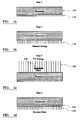
- Figures 1a to 1i illustrate a number of steps of a conventional solid state electronic device fabrication method which will be described by way of background to the present invention.
- a layer of positive photoresist material 110 for example Shipley SPR955CM, is deposited on a substrate 114, which can be Si or GaAs.
- the substrate is then exposed to thermal energy 116 and heated at a temperature of approximately 120°C for approximately 90 seconds in order to stabilise the solvent content in the resist film 110.
- thermal energy 116 is then exposed to thermal energy 116 and heated at a temperature of approximately 120°C for approximately 90 seconds in order to stabilise the solvent content in the resist film 110.
- a mask 118 is positioned over an area at which a feature is to be created and the workpiece is exposed to ultraviolet radiation 120 so as to transfer the mask pattern into the photoresist.
- a typical exposure level is 50mJ/cm 2 .
- a reverse side of the substrate 114 is then heated 122 using a hot plate providing a temperature of approximately 115°C for approximately 240 seconds so as to activate a cross-linking agent in the photoresist.
- An upper surface of the photoresist layer 110 is then exposed to developer solution 124 all over its surface so as to remove the exposed areas of photoresist. This step creates via 126, and the photoresist layer has reentrant or negatively sloped sidewalls 128, 129.
- a layer of metal 130 is then deposited using evaporation so as to create the desired metal track feature 132 on the substrate 114.
- the resist sidewall profile is acceptable in that it allows the photoresist layer to be lifted-off from the substrate in a final lift-off stage to leave the feature 132.
- rotation of the evaporator during the metal deposition stage tends to deposit metal 133 also on the sidewalls 128,129 of the photoresist.
- This sidewall deposited metal often forms an attachment with the metal track 132.
- metal frill type defects 134 are left on the track.
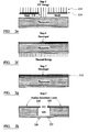
- FIGS. 2a to 2j illustrate steps in a solid state electronic device fabrication method of the present invention. A number of the method steps are the same as or similar to those of the conventional method described above and so will not be described again in great detail.
- Figure 2a shows a wafer substrate 114 on which a feature is to be fabricated and onto which a covering layer of positive photoresist 110 has been spun.
- Shipley SPR955 is an example of a suitable photoresist material.
- a softbake step corresponding to Figure 1b is not the next step. Instead, a MIF (Metal Ion Free) developer solution 210, is used to develop the upper surface of the photoresist layer.
- TMAH ammonium hydroxide is a suitable MIF developer.
- MIB (Metal Ion Bearing) developer solution can be used, such as sodium hydroxide.
- the substrate is then exposed to thermal energy (Fig 2c) in a softbake step using a hotplate to heat the wafer to a temperature of 120°C for approximately 90 seconds so as to create a thin inhibition layer 212 at the upper surface of the photoresist.
- the inhibition layer is typically approximately 1-3 ⁇ m thick. The temperature used in, and duration of, this step determines the thickness or depth of the inhibition layer.
- An imaging exposure step is then performed (Fig 2e) using ultraviolet radiation 214 and a mask 216 to define an aperture 218 corresponding to an area to be exposed on the inhibition layer which will eventually provide an aperture through which a feature will be formed.
- the sizing energy E s is increased compared to prior art methods so as to take into account the effect of the inhibition layer.
- the sizing energy is the energy dose required to achieve the mask critical dimension ("CD", i.e. desired size of the feature).
- CD mask critical dimension
- a typical sizing energy dose would be 300mJ/cm 2 for 600ms.
- Figure 2f illustrates a post exposure bake step analogous to Figure 1d.
- a hotplate is used to heat the wafer at a temperature of approximately 130°C for approximately 90 seconds so as to improve resist contrast and reduce standing waves. Increasing the post exposure bake temperature reduces the resist sensitivity and thereby reduces the critical dimension.
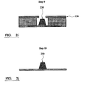
- a developer 218 is then used in a developing step (Fig 2g) to create via 220 and an aperture 222 in the inhibition layer corresponding to the area exposed by mask 216 previously.
- the inhibition layer has parts overhanging the via.
- the surface inhibition layer slows the dissolution rate of the developer. Once the inhibition layer has been breached the dissolution of the resist increases, resulting in the overhanging side wall profile.
- the lateral dimension of the inhibition layer aperture is less than the lateral dimension of the aperture in the photoresist material and so the overhangs 224,225 generate corresponding 'shadow' regions 226,227 on the exposed upper surface of substrate 114.
- the resist side walls are close to vertical with respect to the plane of the substrate and this is controlled by the post exposure bake temperature and time which improves the resist contrast performance.
- Metal is deposited so as to create the desired feature 230 on the substrate.
- the end portions of the inhibition layer over hang the sidewalls of the photoresist layer and so help to prevent metal from being deposited on the side walls.
- the overhang profile prevents metal migrating around the lip of the profile thereby eliminating sidewall deposition and reducing metal defects on the feature after the photoresist layer is lifted-off.
Landscapes
- Physics & Mathematics (AREA)
- General Physics & Mathematics (AREA)
- Photosensitive Polymer And Photoresist Processing (AREA)
- Electrodes Of Semiconductors (AREA)
- Internal Circuitry In Semiconductor Integrated Circuit Devices (AREA)
Applications Claiming Priority (2)
| Application Number | Priority Date | Filing Date | Title |
|---|---|---|---|
| GBGB0213695.0A GB0213695D0 (en) | 2002-06-14 | 2002-06-14 | Fabrication method |
| GB0213695 | 2002-06-14 |
Publications (2)
| Publication Number | Publication Date |
|---|---|
| EP1372191A2 true EP1372191A2 (de) | 2003-12-17 |
| EP1372191A3 EP1372191A3 (de) | 2004-04-07 |
Family
ID=9938587
Family Applications (1)
| Application Number | Title | Priority Date | Filing Date |
|---|---|---|---|
| EP03253753A Withdrawn EP1372191A3 (de) | 2002-06-14 | 2003-06-12 | Verfahren zur Abscheidung einer Struktur auf einem Substrat |
Country Status (3)
| Country | Link |
|---|---|
| US (1) | US20040037999A1 (de) |
| EP (1) | EP1372191A3 (de) |
| GB (2) | GB0213695D0 (de) |
Cited By (1)
| Publication number | Priority date | Publication date | Assignee | Title |
|---|---|---|---|---|
| WO2008028851A1 (en) * | 2006-09-04 | 2008-03-13 | Koninklijke Philips Electronics N.V. | Control of carbon nanostructure growth in an interconnect structure |
Families Citing this family (2)
| Publication number | Priority date | Publication date | Assignee | Title |
|---|---|---|---|---|
| KR101563237B1 (ko) * | 2007-06-01 | 2015-10-26 | 가부시키가이샤 한도오따이 에네루기 켄큐쇼 | 제조장치 및 발광장치 제작방법 |
| US20250093778A1 (en) * | 2023-09-18 | 2025-03-20 | Tokyo Electron Limited | Method for area selective deposition on extreme ultra-violet (euv) photoresists |
Family Cites Families (17)
| Publication number | Priority date | Publication date | Assignee | Title |
|---|---|---|---|---|
| JPS5811512B2 (ja) * | 1979-07-25 | 1983-03-03 | 超エル・エス・アイ技術研究組合 | パタ−ン形成方法 |
| NL8004573A (nl) * | 1979-09-19 | 1981-03-23 | Gen Electric | Werkwijze voor het vervaardigen van samengestelde voorwerpen. |
| JPS5778141A (en) * | 1980-10-31 | 1982-05-15 | Fujitsu Ltd | Forming method for conductor pattern |
| JPS57199222A (en) * | 1981-06-02 | 1982-12-07 | Nippon Telegr & Teleph Corp <Ntt> | Control of cross-section of lift-off resist stencil |
| US4687541A (en) * | 1986-09-22 | 1987-08-18 | Rockwell International Corporation | Dual deposition single level lift-off process |
| JPH01163095A (ja) * | 1987-09-07 | 1989-06-27 | Toshiba Corp | Icカード収納ケースの製造方法 |
| JPH03119720A (ja) * | 1989-10-03 | 1991-05-22 | Nippon Telegr & Teleph Corp <Ntt> | リフトオフ加工用ホトレジスト、リフトオフ加工用ホトレジストのパターン形成方法及びリフトオフ方法 |
| JPH03235322A (ja) * | 1990-02-13 | 1991-10-21 | Nec Corp | レジストパターン形成方法 |
| JPH0629239A (ja) * | 1992-02-27 | 1994-02-04 | Eastman Kodak Co | リフト−オフプロセスを利用した半導体素子におけるセルフアライン拡散バリアの製造方法及び拡散バリアを有する半導体素子 |
| DE4401590A1 (de) * | 1994-01-20 | 1995-07-27 | Siemens Ag | Verfahren zur Herstellung strukturierter Metallisierungen |
| JPH0992605A (ja) * | 1995-09-27 | 1997-04-04 | Matsushita Electron Corp | レジストパターンの形成方法及びこの方法を用いた半導体装置の製造方法 |
| US5705432A (en) * | 1995-12-01 | 1998-01-06 | Hughes Aircraft Company | Process for providing clean lift-off of sputtered thin film layers |
| JPH1197328A (ja) * | 1997-09-17 | 1999-04-09 | Toshiba Corp | レジストパターンの形成方法 |
| US6372414B1 (en) * | 1999-03-12 | 2002-04-16 | Clariant Finance (Bvi) Limited | Lift-off process for patterning fine metal lines |
| CA2337087C (en) * | 2000-03-08 | 2006-06-06 | Canon Kabushiki Kaisha | Magnetic toner, process for production thereof, and image forming method, apparatus and process cartridge using the toner |
| JP2002025935A (ja) * | 2000-07-11 | 2002-01-25 | Advantest Corp | 導体部材形成方法、パターン形成方法 |
| US7060637B2 (en) * | 2003-05-12 | 2006-06-13 | Micron Technology, Inc. | Methods of forming intermediate semiconductor device structures using spin-on, photopatternable, interlayer dielectric materials |
-
2002
- 2002-06-14 GB GBGB0213695.0A patent/GB0213695D0/en not_active Ceased
-
2003
- 2003-06-12 GB GB0313560A patent/GB2392009A/en not_active Withdrawn
- 2003-06-12 EP EP03253753A patent/EP1372191A3/de not_active Withdrawn
- 2003-06-13 US US10/461,527 patent/US20040037999A1/en not_active Abandoned
Cited By (2)
| Publication number | Priority date | Publication date | Assignee | Title |
|---|---|---|---|---|
| WO2008028851A1 (en) * | 2006-09-04 | 2008-03-13 | Koninklijke Philips Electronics N.V. | Control of carbon nanostructure growth in an interconnect structure |
| US8399772B2 (en) | 2006-09-04 | 2013-03-19 | Nxp B.V. | Control of carbon nanostructure growth in an interconnect structure |
Also Published As
| Publication number | Publication date |
|---|---|
| US20040037999A1 (en) | 2004-02-26 |
| EP1372191A3 (de) | 2004-04-07 |
| GB0213695D0 (en) | 2002-07-24 |
| GB0313560D0 (en) | 2003-07-16 |
| GB2392009A (en) | 2004-02-18 |
Similar Documents
| Publication | Publication Date | Title |
|---|---|---|
| CA1072389A (en) | Methods for forming thick self-supporting masks | |
| EP0341843A2 (de) | Verfahren zur Herstellung eines Leitermusters | |
| US8546048B2 (en) | Forming sloped resist, via, and metal conductor structures using banded reticle structures | |
| JPH0147008B2 (de) | ||
| EP0348962A2 (de) | Feinstruktur-Herstellungsverfahren | |
| US20080008967A1 (en) | Utilization of electric field with isotropic development in photolithography | |
| EP1372191A2 (de) | Verfahren zur Abscheidung einer Struktur auf einem Substrat | |
| JP2000164594A (ja) | 配線パターンの形成方法 | |
| JP2002151381A (ja) | パターン形成方法 | |
| JPH06267843A (ja) | パターン形成方法 | |
| TW200300962A (en) | Improved lithography process for transparent substrates | |
| JP3330214B2 (ja) | 多層レジストパターンの形成方法,及び半導体装置の製造方法 | |
| JP2716957B2 (ja) | 導電性微細パターンの形成方法 | |
| JP2723260B2 (ja) | 微細パターン形成方法 | |
| JPH03138922A (ja) | 微細パターン形成方法 | |
| JPH08220771A (ja) | パターン形成方法 | |
| JPH1154460A (ja) | 電導性構造を製造する方法 | |
| JP3398603B2 (ja) | レジストパターンの形成方法及び半導体装置の製造方法 | |
| JPH07130751A (ja) | アルミ系金属膜のパターニング方法 | |
| JPS5857908B2 (ja) | 薄膜構造体の形成方法 | |
| JPH04291733A (ja) | GaAsデバイス及びT字型ゲート電極の作成方法 | |
| JP2002025935A (ja) | 導体部材形成方法、パターン形成方法 | |
| JP2009198587A (ja) | レジストパターン形成方法、及びそれを利用した金属パターン形成方法 | |
| JP2005136430A (ja) | パターン形成方法 | |
| JPH08191044A (ja) | レジストパターン形成方法 |
Legal Events
| Date | Code | Title | Description |
|---|---|---|---|
| PUAI | Public reference made under article 153(3) epc to a published international application that has entered the european phase |
Free format text: ORIGINAL CODE: 0009012 |
|
| AK | Designated contracting states |
Kind code of ref document: A2 Designated state(s): AT BE BG CH CY CZ DE DK EE ES FI FR GB GR HU IE IT LI LU MC NL PT RO SE SI SK TR |
|
| AX | Request for extension of the european patent |
Extension state: AL LT LV MK |
|
| PUAL | Search report despatched |
Free format text: ORIGINAL CODE: 0009013 |
|
| RIC1 | Information provided on ipc code assigned before grant |
Ipc: 7G 03F 7/38 B Ipc: 7H 01L 21/308 B Ipc: 7H 01L 21/027 A |
|
| AK | Designated contracting states |
Kind code of ref document: A3 Designated state(s): AT BE BG CH CY CZ DE DK EE ES FI FR GB GR HU IE IT LI LU MC NL PT RO SE SI SK TR |
|
| AX | Request for extension of the european patent |
Extension state: AL LT LV MK |
|
| AKX | Designation fees paid | ||
| REG | Reference to a national code |
Ref country code: DE Ref legal event code: 8566 |
|
| STAA | Information on the status of an ep patent application or granted ep patent |
Free format text: STATUS: THE APPLICATION IS DEEMED TO BE WITHDRAWN |
|
| 18D | Application deemed to be withdrawn |
Effective date: 20041008 |