EP1376461A2 - Carte memoire - Google Patents
Carte memoire Download PDFInfo
- Publication number
- EP1376461A2 EP1376461A2 EP03019599A EP03019599A EP1376461A2 EP 1376461 A2 EP1376461 A2 EP 1376461A2 EP 03019599 A EP03019599 A EP 03019599A EP 03019599 A EP03019599 A EP 03019599A EP 1376461 A2 EP1376461 A2 EP 1376461A2
- Authority
- EP
- European Patent Office
- Prior art keywords
- write
- memory card
- main body
- nonwrite
- setting element
- Prior art date
- Legal status (The legal status is an assumption and is not a legal conclusion. Google has not performed a legal analysis and makes no representation as to the accuracy of the status listed.)
- Ceased
Links
Images


Classifications
-
- G—PHYSICS
- G06—COMPUTING OR CALCULATING; COUNTING
- G06K—GRAPHICAL DATA READING; PRESENTATION OF DATA; RECORD CARRIERS; HANDLING RECORD CARRIERS
- G06K19/00—Record carriers for use with machines and with at least a part designed to carry digital markings
- G06K19/06—Record carriers for use with machines and with at least a part designed to carry digital markings characterised by the kind of the digital marking, e.g. shape, nature, code
- G06K19/067—Record carriers with conductive marks, printed circuits or semiconductor circuit elements, e.g. credit or identity cards also with resonating or responding marks without active components
- G06K19/07—Record carriers with conductive marks, printed circuits or semiconductor circuit elements, e.g. credit or identity cards also with resonating or responding marks without active components with integrated circuit chips
- G06K19/077—Constructional details, e.g. mounting of circuits in the carrier
- G06K19/07743—External electrical contacts
-
- G—PHYSICS
- G06—COMPUTING OR CALCULATING; COUNTING
- G06F—ELECTRIC DIGITAL DATA PROCESSING
- G06F1/00—Details not covered by groups G06F3/00 - G06F13/00 and G06F21/00
- G06F1/16—Constructional details or arrangements
-
- G—PHYSICS
- G06—COMPUTING OR CALCULATING; COUNTING
- G06K—GRAPHICAL DATA READING; PRESENTATION OF DATA; RECORD CARRIERS; HANDLING RECORD CARRIERS
- G06K19/00—Record carriers for use with machines and with at least a part designed to carry digital markings
- G06K19/06—Record carriers for use with machines and with at least a part designed to carry digital markings characterised by the kind of the digital marking, e.g. shape, nature, code
- G06K19/067—Record carriers with conductive marks, printed circuits or semiconductor circuit elements, e.g. credit or identity cards also with resonating or responding marks without active components
- G06K19/07—Record carriers with conductive marks, printed circuits or semiconductor circuit elements, e.g. credit or identity cards also with resonating or responding marks without active components with integrated circuit chips
- G06K19/073—Special arrangements for circuits, e.g. for protecting identification code in memory
-
- G—PHYSICS
- G06—COMPUTING OR CALCULATING; COUNTING
- G06K—GRAPHICAL DATA READING; PRESENTATION OF DATA; RECORD CARRIERS; HANDLING RECORD CARRIERS
- G06K19/00—Record carriers for use with machines and with at least a part designed to carry digital markings
- G06K19/06—Record carriers for use with machines and with at least a part designed to carry digital markings characterised by the kind of the digital marking, e.g. shape, nature, code
- G06K19/067—Record carriers with conductive marks, printed circuits or semiconductor circuit elements, e.g. credit or identity cards also with resonating or responding marks without active components
- G06K19/07—Record carriers with conductive marks, printed circuits or semiconductor circuit elements, e.g. credit or identity cards also with resonating or responding marks without active components with integrated circuit chips
- G06K19/077—Constructional details, e.g. mounting of circuits in the carrier
- G06K19/0772—Physical layout of the record carrier
- G06K19/07732—Physical layout of the record carrier the record carrier having a housing or construction similar to well-known portable memory devices, such as SD cards, USB or memory sticks
-
- Y—GENERAL TAGGING OF NEW TECHNOLOGICAL DEVELOPMENTS; GENERAL TAGGING OF CROSS-SECTIONAL TECHNOLOGIES SPANNING OVER SEVERAL SECTIONS OF THE IPC; TECHNICAL SUBJECTS COVERED BY FORMER USPC CROSS-REFERENCE ART COLLECTIONS [XRACs] AND DIGESTS
- Y10—TECHNICAL SUBJECTS COVERED BY FORMER USPC
- Y10S—TECHNICAL SUBJECTS COVERED BY FORMER USPC CROSS-REFERENCE ART COLLECTIONS [XRACs] AND DIGESTS
- Y10S439/00—Electrical connectors
- Y10S439/945—Adapter for pcb or cartridge
-
- Y—GENERAL TAGGING OF NEW TECHNOLOGICAL DEVELOPMENTS; GENERAL TAGGING OF CROSS-SECTIONAL TECHNOLOGIES SPANNING OVER SEVERAL SECTIONS OF THE IPC; TECHNICAL SUBJECTS COVERED BY FORMER USPC CROSS-REFERENCE ART COLLECTIONS [XRACs] AND DIGESTS
- Y10—TECHNICAL SUBJECTS COVERED BY FORMER USPC
- Y10S—TECHNICAL SUBJECTS COVERED BY FORMER USPC CROSS-REFERENCE ART COLLECTIONS [XRACs] AND DIGESTS
- Y10S439/00—Electrical connectors
- Y10S439/946—Memory card cartridge
Definitions
- the present invention relates to a memory card incorporating a write/nonwrite setting means for preventing erroneous erasure or erroneous rewriting of a stored content.
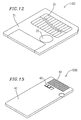
- FIG 13 is a perspective view showing a conventional memory card 1200 incorporating a write/nonwrite setting means which is realized by a switch 43 .
- reference numeral 41 denotes a main body of the memory card
- reference numeral 42 denotes a terminal which is integrally formed with the main body 41 of the memory card
- reference numeral 43 denotes a switch.
- the conventional memory card 1100 which incorporates a write/nonwrite setting means realized by the reflective sheet 33 , does not have a mechanical structure for the write/nonwrite setting means.
- the reflective sheet 33 is effective in achieving a more compact and thinner main body 31 of the memory card.
- manipulation of the write/nonwrite setting means is inconvenient because the write/nonwrite state of the memory card is set by the application and the peeling off of the reflective sheet 33 .
- the write/nonwrite state of the memory card is set by the switching of the switch 43.
- manipulation for setting the write/nonwrite state of the memory card is simple.
- there is a limit to a decrease in the size and thickness of the main body 41 of the memory card because the main body 41 of the memory card incorporates a switch.
- a memory card includes: a main body of the memory card in which a notched section is formed; a semiconductor memory in which data can be at least written; a terminal provided in the main body of the memory card for electrically connecting the semiconductor memory to an external device; and a write/nonwrite setting element for setting the write/nonwrite state of the data in the semiconductor memory, the write/nonwrite setting element being slidably fitted in the notched section, wherein the main body of the memory card includes an upper main body and a lower main body; at least one of the upper main body and the lower main body has an elastic guide formed within the notched section; the write/nonwrite setting element is slidably fitted in the elastic guide and is sandwiched between the upper main body and the lower main body; the write/nonwrite setting element is positioned such that a portion of the write/nonwrite setting element covers a portion of the notched section; the write/nonwrite setting element slides along the elastic guide so as to set the write/nonwrite state of the data in the
- the engagement portion may include a protrusion which is formed so as to engagedly stop the write/nonwrite setting element; and the write/nonwrite setting element may ride over the protrusion so as to be engagedly stopped at one of the opposite ends of the elastic guide, thereby selecting a position of the notched section which is covered with the write/nonwrite setting element.
- the engagement portion may include a first engagement portion which is formed by a protrusion or a cavity; the write/nonwrite setting element may include a second engagement portion which is formed by a cavity or a protrusion; and the second engagement portion may be engagedly stopped by the first engagement portion, whereby the write/nonwrite setting element may select a position of the notched section which is covered with the write/nonwrite setting element.
- One of the upper main body and the lower main body may have a slit which is formed in the elastic guide; and the write/nonwrite setting element may fit in the slit.
- the write/nonwrite setting element may include: a manipulation portion which covers the notched section so as to achieve setting of the write/nonwrite state and which is used as a manually-operated shift knob; an anti-disengagement portion which is fitted in the slit; and a slide contact portion which connects the manipulation portion with the anti-disengagement portion and which slidably contacts the elastic guide.
- the other of the upper main body and the lower main body may have a reentrant groove at a position such as to face the slit; and the write/nonwrite setting element may fit in the slit and the reentrant groove.
- One of the upper main body and the lower main body may have a labeling region on which a label is attached so as to cover the slit.
- At least one of the upper main body and the lower main body may have a reentrant groove which is formed so as to fit with the write/nonwrite setting element.
- the memory card may further include a switch for electrically switching the write/nonwrite state of the data, the switch being provided inside the main body of the memory card, wherein: the switch may have an activation portion which is provided so as to extend from the switch toward the write/nonwrite setting element; and the activation portion may electrically switch the write/nonwrite state of the data in response to a sliding movement of the write/nonwrite setting element.
- the memory card may further include a contact point for electrically switching the write/nonwrite state of the data, the contact point being provided inside the main body of the memory card, wherein the write/nonwrite setting element may have a contact piece provided at a position corresponding to the contact point.
- the memory card may further include a print substrate on which the semiconductor memory is mounted, wherein the contact point may be formed on the print substrate.
- the elastic guide maybe formed such that the elastic force of the elastic guide is affected in a direction from the contact piece to the contact point.
- the upper main body and the lower main body may form a slide hole within the notched section;
- the elastic guide may include a groove formed within the slide hole in at least one of the upper main body and the lower main body;
- the write/nonwrite setting element may have a fitting portion which is inserted into the slide hole and is fitted in the groove;
- the fitting portion may include a maximum width section which has a width greater than a width of the slide hole such that the fitting portion can be inserted into the slide hole by means of elastic deformation of the upper main body and the lower main body; and the engagement portion may be formed in the groove.
- a tip section of the fitting portion may have a width smaller than that of the slide hole; the fitting portion may have an inclined face extending from the tip section to the maximum width section; and the write/nonwrite setting element may be inserted in the slide hole while the inclined face expands the slide hole until the fitting portion is fitted into the groove, whereby the write/nonwrite setting element may be attached to the main body of the memory card.
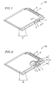
- Figure 1 is a perspective view showing a lower surface side of an assembled memory card 100 according to embodiment 1 of the present invention.
- Figure 2 is a perspective view showing the memory card 100 in which a lower main body is partially cut away.
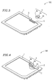
- Figure 3 is a perspective view showing an upper surface side of the partially-exploded memory card 100.
- Figure 4 is a perspective view showing the memory card 100 in which an upper main body is partially cut away.
- Figure 5 is a cross-sectional view showing the memory card 100 taken along line A-A in Figure 1 .
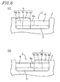
- Figures 6(a) and 6(b) illustrate manipulation of a write/nonwrite setting element of the memory card 100 .
- Figures 7(a) and 7(b) illustrates detection of the setting of the write/nonwrite setting element in the memory card 100.
- an elastic guide 6 and a slit 5 are formed in the upper main body 1 of the memory card within the notched section 3 , and a groove 7 is formed in the lower main body 2 at a position which faces the slit 5 .
- the write/nonwrite setting element 4 is slidably fitted in the slit 5 , the groove 7 , and the elastic guide 6 , and is sandwiched by the upper and lower main bodies 1 and 2 of the memory card.
- the write/nonwrite setting element 4 is positioned so that a portion of the setting element 4 meets with the notched section 3 formed in the upper main body 1 of the memory card and covers a portion of the notched section 3 . Sliding movement of the setting element 4 selects a position at which the notched section 3 is covered.
- the write/nonwrite setting element 4 covers a portion of the notched section 3 so as to set the write/nonwrite state of the memory card.
- the write/nonwrite setting element 4 includes: a manipulation portion 4a used as a shift knob which is manually operated so as to set the write/nonwrite state of the memory card; an anti-disengagement portion 4b which is fitted in the slit 5 and the groove 7 ; and a slide contact portion 4c which connects the manipulation portion 4a with the anti-disengagement portion 4b and which slidably contacts the elastic guide 6 .
- the write/nonwrite setting element 4 fits in the upper main body 1 of the memory card, in which the slit 5 is formed, and is covered with the lower main body 2 of the memory card, in which the groove 7 is formed, such that the anti-disengagement portion 4b fits in the slit 5 and the groove 7 , and the slide contact portion 4c is slidably held between the elastic guide 6 and the lower main body 2 of the memory card.
- the elastic guide 6 provided in the upper main body 1 of the memory card has an engagement portion in a substantially central area thereof, which is formed by a protrusion 6a .
- the slide contact portion 4c of the write/nonwrite setting element 4 is provided so as to ride over the protrusion 6a so as to be engagedly stopped at the opposite sides of the elastic guide 6 , thereby selecting a position where the write/nonwrite setting element 4 covers the notched section 3 . That is, between the elastic guide 6 formed in the upper main body 1 of the memory card and the write/nonwrite setting element 4 , an engagement portion for stopping sliding movement of the write/nonwrite setting element 4 along the elastic guide 6 is provided.
- a terminal 9 for establishing an electrical connection with a device is integrally formed in a slit portion 8 of the lower main body 2 of the memory card.
- the memory card Inside the main body, the memory card includes a substrate 11 which has a semiconductor memory 10 mounted thereon having a rewritable content. The content stored in the semiconductor memory 10 is read out or rewritten through the terminal 9 by an electrically-connected device (not shown).
- the memory card has the write/nonwrite setting means (further described later) for preventing erroneous erasure or erroneous overwriting of a stored content.
- Reference numeral 12 denotes a labeling region, which is formed in a surface of the upper main body 1 of the memory card so as to have a recessed shape. As shown in Figure 5 , in the labeling region 12, a label 12a on which predetermined presentation items about the memory card are printed is attached. In this example, the anti-disengagement portion 4b of the write/nonwrite setting element 4 is formed so as not to extend beyond the end edge of the slit 5 . With such a structure, the label 12a is prevented from being peeled off .
- the write/nonwrite setting element 4 is sandwiched, together with the substrate 11 having the semiconductor memory 10 mounted thereon, by the upper main body 1 and the lower main body 2 of the memory card, whereby the write/nonwrite setting element 4 is held in the main body assembly 51 of the memory card.
- the write/nonwrite setting element 4 is held at a predetermined position between the upper main body 1 and the lower main body 2 of the memory card such that the setting element 4 can be guided by the slit 5 , the elastic guide 6 , and the groove 7 .
- the circumferences of the upper main body 1 and the lower main body 2 of the memory card are welded or adhered to each other except for the notched section 3 .
- the write/nonwrite setting element 4 is provided so as to be held between the upper main body 1 and the lower main body 2 of the memory card, so that the manipulation portion 4a thereof covers a portion of the notched section 3 .
- substantially a right or left half of the notched section 3 is covered.
- the left half is covered, and the covered portion has a generally integral shape with the external shape of the upper main body 1 of the memory card.
- the uncovered, remaining right half of the notched section 3 forms a flat rectangular recess in the main body of the memory card.
- reference numeral 22 denotes a device in which a memory card of this embodiment is insertively connected.
- Reference numeral 21 denotes a detection switch provided in the device 22 .
- the detection switch 21 includes a detection section 23 and a contact-point element 24.
- the write/nonwrite setting element 4 covers the left half of the notched section 3 , as shown in Figure 6(a), and it is assumed that the memory card is writable when the write/nonwrite setting element 4 is placed at the left side of the notched section 3 .
- the detection section 23 of the detection switch 21 is raised so that the contact-point element 24 is closed.
- the device 22 detects that the contact-point element 24 is closed, thereby recognizing that the memory card is writable.
- the memory card is nonwritable when the write/nonwrite setting element 4 is placed at the right side of the notched section 3 .
- the detection section 23 of the detection switch 21 is not raised so that the contact-point element 24 is open.
- the device 22 detects that the contact-point element 24 is open, thereby recognizing that the memory card is nonwritable.
- the basic structure of the memory card of embodiment 2 is the same as that of the memory card of embodiment 1.
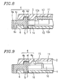
- a switch 13 is mounted on a substrate 11 which is provided inside the memory card, and the switch 13 has an activation portion 13a which extends toward the write/nonwrite setting element 4.
- the write/nonwrite setting element 4 has an operation portion 4e, which is placed so as to engage with the activation portion 13a of the switch 13.
- a space bis provided between the upper main body 1 and the lower main body 2 of the memory card, in which the operation portion 4e and the activation portion 13a are slid or moved.
- Figure 9 shows a cross-section of a memory card incorporating a contact section according to embodiment 3 of the present invention.
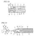
- Figure 10 shows a cross-section of a portion of a memory card according to embodiment 4 of the present invention, in which a write/nonwrite setting element 4 is provided.
- the basic structure of the memory card of embodiment 4 is the same as that of the memory card of embodiment 1.
- the upper main body 1 of the memory card has a reentrant groove 17 in place of the slit 5 of Figure 1 .
- the anti-disengagement portion 4b of the write/nonwrite setting element 4 fits in the reentrant groove 17 and the reentrant groove 7 formed in the lower main body 2 of the memory card.
- Figure 11 shows a cross-section of a portion of a memory card according to embodiment 5 of the present invention, in which a write/nonwrite setting element is provided.
- the write/nonwrite setting element 4 has a fitting portion 4h which fits in the grooves 19 and 20 when the setting element 4 is inserted into the slide hole 18 formed by the upper and lower main bodies 1 and 2 of the memory card.
- Width D2 of a maximum width section 4j of the fitting portion 4h is greater than width D1 of the slide hole 18.
- Width D3 of a tip section 4k of the fitting portion 4h is smaller than width D1 of the slide hole 18 .
- the fitting portion 4h has an inclined face 4m extending from the tip section 4k to the maximum width section 4j.
- the write/nonwrite setting element 4 is forcedly inserted into the slide hole 18 along the direction indicated by arrow A1, so as to fit in the grooves 19 and 20.
- the inclined face 4m expands the slide hole 18 formed by the upper and lower main bodies 1 and 2 of the memory card.
- the write/nonwrite setting element 4 is further inserted, while the upper and lower main bodies 1 and 2 are elastically deformed, until the fitting portion 4h fits in the grooves 19 and 20.
- the write/nonwrite setting element 4 After the write/nonwrite setting element 4 has been fitted in the memory card, the write/nonwrite setting element 4 is positioned by means of the engagement portion 21 formed in the grooves 19 and 20 in a similar manner described in conjunction with the memory cards of the previous embodiments.
- a write/nonwrite setting element is slidably fitted in a notched section provided at a side portion of a main body of a memory card.
- Setting of the write/nonwrite state of the memory card is achieved by selecting a portion of the notched section which is covered with the write/nonwrite setting element by means of a sliding movement of the write/nonwrite setting element.
- the memory card does not have any protrusion over its side face, and the thickness of the memory card is maintained so as to be thin.
Landscapes
- Engineering & Computer Science (AREA)
- Computer Hardware Design (AREA)
- Theoretical Computer Science (AREA)
- Physics & Mathematics (AREA)
- General Physics & Mathematics (AREA)
- Microelectronics & Electronic Packaging (AREA)
- General Engineering & Computer Science (AREA)
- Computer Security & Cryptography (AREA)
- Human Computer Interaction (AREA)
- Credit Cards Or The Like (AREA)
- Storage Device Security (AREA)
- Coupling Device And Connection With Printed Circuit (AREA)
- Details Of Connecting Devices For Male And Female Coupling (AREA)
Applications Claiming Priority (3)
| Application Number | Priority Date | Filing Date | Title |
|---|---|---|---|
| JP23673499 | 1999-08-24 | ||
| JP23673499 | 1999-08-24 | ||
| EP00953547A EP1207493B1 (fr) | 1999-08-24 | 2000-08-21 | Carte memoire |
Related Parent Applications (1)
| Application Number | Title | Priority Date | Filing Date |
|---|---|---|---|
| EP00953547A Division EP1207493B1 (fr) | 1999-08-24 | 2000-08-21 | Carte memoire |
Publications (2)
| Publication Number | Publication Date |
|---|---|
| EP1376461A2 true EP1376461A2 (fr) | 2004-01-02 |
| EP1376461A3 EP1376461A3 (fr) | 2004-02-25 |
Family
ID=17005005
Family Applications (3)
| Application Number | Title | Priority Date | Filing Date |
|---|---|---|---|
| EP03019599A Ceased EP1376461A3 (fr) | 1999-08-24 | 2000-08-21 | Carte memoire |
| EP03019600A Expired - Lifetime EP1411464B1 (fr) | 1999-08-24 | 2000-08-21 | Carte à mémoire |
| EP00953547A Expired - Lifetime EP1207493B1 (fr) | 1999-08-24 | 2000-08-21 | Carte memoire |
Family Applications After (2)
| Application Number | Title | Priority Date | Filing Date |
|---|---|---|---|
| EP03019600A Expired - Lifetime EP1411464B1 (fr) | 1999-08-24 | 2000-08-21 | Carte à mémoire |
| EP00953547A Expired - Lifetime EP1207493B1 (fr) | 1999-08-24 | 2000-08-21 | Carte memoire |
Country Status (7)
| Country | Link |
|---|---|
| US (4) | US6580615B1 (fr) |
| EP (3) | EP1376461A3 (fr) |
| KR (2) | KR100591872B1 (fr) |
| CN (2) | CN1275196C (fr) |
| DE (2) | DE60005976T2 (fr) |
| TW (1) | TW480448B (fr) |
| WO (1) | WO2001015072A1 (fr) |
Families Citing this family (74)
| Publication number | Priority date | Publication date | Assignee | Title |
|---|---|---|---|---|
| KR100473308B1 (ko) | 1995-01-31 | 2005-03-14 | 가부시끼가이샤 히다치 세이사꾸쇼 | 불휘발성 메모리 장치 |
| US20040157612A1 (en) * | 1997-04-25 | 2004-08-12 | Minerva Industries, Inc. | Mobile communication and stethoscope system |
| US7321783B2 (en) * | 1997-04-25 | 2008-01-22 | Minerva Industries, Inc. | Mobile entertainment and communication device |
| JP3173438B2 (ja) * | 1997-06-04 | 2001-06-04 | ソニー株式会社 | メモリカード及び装着装置 |
| US6802453B1 (en) * | 1997-06-04 | 2004-10-12 | Sony Corporation | External storage apparatus and control apparatus thereof, and data transmission reception apparatus |
| US6634561B1 (en) * | 1999-06-24 | 2003-10-21 | Sandisk Corporation | Memory card electrical contact structure |
| US7872871B2 (en) * | 2000-01-06 | 2011-01-18 | Super Talent Electronics, Inc. | Molding methods to manufacture single-chip chip-on-board USB device |
| US7264992B2 (en) * | 2004-08-06 | 2007-09-04 | Paul Hsueh | Removable flash integrated memory module card and method of manufacture |
| US7830666B2 (en) | 2000-01-06 | 2010-11-09 | Super Talent Electronics, Inc. | Manufacturing process for single-chip MMC/SD flash memory device with molded asymmetric circuit board |
| US8141240B2 (en) | 1999-08-04 | 2012-03-27 | Super Talent Electronics, Inc. | Manufacturing method for micro-SD flash memory card |
| EP1376461A3 (fr) * | 1999-08-24 | 2004-02-25 | Matsushita Electric Industrial Co., Ltd. | Carte memoire |
| US7535088B2 (en) * | 2000-01-06 | 2009-05-19 | Super Talent Electronics, Inc. | Secure-digital (SD) flash card with slanted asymmetric circuit board |
| US20080286990A1 (en) * | 2003-12-02 | 2008-11-20 | Super Talent Electronics, Inc. | Direct Package Mold Process For Single Chip SD Flash Cards |
| JP4082913B2 (ja) * | 2002-02-07 | 2008-04-30 | 株式会社ルネサステクノロジ | メモリシステム |
| US7092256B1 (en) | 2002-04-26 | 2006-08-15 | Sandisk Corporation | Retractable card adapter |
| JP2003346109A (ja) * | 2002-05-22 | 2003-12-05 | Toshiba Corp | Icカード及び半導体集積回路装置パッケージ |
| JP4238580B2 (ja) * | 2002-11-15 | 2009-03-18 | ソニー株式会社 | データ記憶装置、データ記録システム |
| DE20302251U1 (de) * | 2003-02-12 | 2003-04-17 | D & C Technology Co., Ltd., Hsin Tien, Taipeh | Klemmenleiste für eine Speicherkarte |
| US7094633B2 (en) * | 2003-06-23 | 2006-08-22 | Sandisk Corporation | Method for efficiently producing removable peripheral cards |
| TWD100978S1 (zh) | 2003-10-13 | 2004-10-21 | 希旺科技股份有限公司 | 電子記憶卡(一) |
| US8102657B2 (en) | 2003-12-02 | 2012-01-24 | Super Talent Electronics, Inc. | Single shot molding method for COB USB/EUSB devices with contact pad ribs |
| US8998620B2 (en) * | 2003-12-02 | 2015-04-07 | Super Talent Technology, Corp. | Molding method for COB-EUSB devices and metal housing package |
| US7152801B2 (en) * | 2004-04-16 | 2006-12-26 | Sandisk Corporation | Memory cards having two standard sets of contacts |
| US7487265B2 (en) * | 2004-04-16 | 2009-02-03 | Sandisk Corporation | Memory card with two standard sets of contacts and a hinged contact covering mechanism |
| US7032827B2 (en) * | 2004-06-18 | 2006-04-25 | Super Talent Electronics, Inc. | Combination SD/MMC flash memory card with thirteen contact pads |
| US20050281010A1 (en) * | 2004-06-18 | 2005-12-22 | Super Talent Electronics, Inc. | Contact pad arrangement for integrated SD/MMC system |
| US20080195817A1 (en) * | 2004-07-08 | 2008-08-14 | Super Talent Electronics, Inc. | SD Flash Memory Card Manufacturing Using Rigid-Flex PCB |
| US7804163B2 (en) * | 2004-08-06 | 2010-09-28 | Supertalent Electronics, Inc. | Seamless secured digital card manufacturing methods with male guide and female switch |
| BRPI0510494B8 (pt) | 2004-07-12 | 2022-06-28 | Kk Toshiba Toshiba Corporation | Dispositivo de armazenagem e aparelho hospedeiro |
| US7795714B2 (en) * | 2004-08-06 | 2010-09-14 | Supertalent Electronics, Inc. | Two step molding process secured digital card manufacturing method and apparatus |
| JP2006236261A (ja) * | 2005-02-28 | 2006-09-07 | Renesas Technology Corp | メモリカード用アダプタおよびメモリカード |
| CN100391321C (zh) * | 2005-03-04 | 2008-05-28 | 威刚科技股份有限公司 | 滑套式的可携带快闪存储装置 |
| CN100392674C (zh) * | 2005-03-04 | 2008-06-04 | 威刚科技股份有限公司 | 存储卡模块 |
| US20060231634A1 (en) * | 2005-04-15 | 2006-10-19 | Power Digital Card Co., Ltd. | Memory card structure |
| USD552099S1 (en) * | 2005-05-24 | 2007-10-02 | Renesas Technology Corporation | Memory card |
| US7710736B2 (en) | 2005-08-02 | 2010-05-04 | Sandisk Corporation | Memory card with latching mechanism for hinged cover |
| US7193161B1 (en) * | 2006-02-15 | 2007-03-20 | Sandisk Corporation | SiP module with a single sided lid |
| US8089776B2 (en) * | 2006-06-19 | 2012-01-03 | Sony Ericsson Mobile Communications Ab | Side switch for a contact exposed on an edge of a circuit board and method |
| US7367817B1 (en) * | 2006-11-09 | 2008-05-06 | Chin-Chun Liu | Housing of an electrical card |
| US8254134B2 (en) | 2007-05-03 | 2012-08-28 | Super Talent Electronics, Inc. | Molded memory card with write protection switch assembly |
| US8102658B2 (en) * | 2007-07-05 | 2012-01-24 | Super Talent Electronics, Inc. | Micro-SD to secure digital adaptor card and manufacturing method |
| JP5065821B2 (ja) * | 2007-09-13 | 2012-11-07 | 任天堂株式会社 | 装置掛止用フックおよび付属装置 |
| US9084935B2 (en) * | 2007-09-13 | 2015-07-21 | Nintendo Co., Ltd. | Attachment device for an electronic apparatus |
| US7485005B1 (en) * | 2007-11-09 | 2009-02-03 | Jess-Link Products Co., Ltd. | Adapter card structure |
| USD588597S1 (en) * | 2007-12-17 | 2009-03-17 | Panasonic Corporation | IC memory card |
| USD588133S1 (en) * | 2007-12-17 | 2009-03-10 | Panasonic Corporation | IC memory card |
| USD588134S1 (en) * | 2008-01-11 | 2009-03-10 | Panasonic Corporation | IC memory card |
| US8085501B2 (en) | 2008-01-29 | 2011-12-27 | Imation Corp. | Reader including an interposer that prevents coupling with write-protected data cartridges |
| USD588599S1 (en) * | 2008-04-01 | 2009-03-17 | Panasonic Corporation | IC memory card |
| USD588598S1 (en) * | 2008-04-01 | 2009-03-17 | Panasonic Corporation | IC memory card |
| USD588135S1 (en) * | 2008-04-01 | 2009-03-10 | Panasonic Corporation | IC memory card |
| KR20100001259A (ko) * | 2008-06-26 | 2010-01-06 | 삼성전자주식회사 | 메모리 카드 및 그의 제조방법 |
| US7630203B1 (en) * | 2008-09-17 | 2009-12-08 | Ardi Technology Corporation | IC card |
| USD632298S1 (en) * | 2008-10-23 | 2011-02-08 | Depaula Andrew C | Electronic memory device |
| KR101024201B1 (ko) * | 2009-07-09 | 2011-03-23 | 비아이 이엠티 주식회사 | 메모리카드 스위치의 자동조립장치 |
| USD638431S1 (en) * | 2009-10-20 | 2011-05-24 | Sandisk Corporation | MicroSD memory card with a semi-transparent color surface |
| USD628202S1 (en) * | 2009-10-20 | 2010-11-30 | Sandisk Corporation | MicroSD memory card with different color surfaces |
| US8690283B2 (en) | 2009-10-20 | 2014-04-08 | Sandisk Il Ltd. | Method and system for printing graphical content onto a plurality of memory devices and for providing a visually distinguishable memory device |
| US8561910B2 (en) | 2009-10-22 | 2013-10-22 | Intellipaper, Llc | Memory programming methods and memory programming devices |
| US8523071B2 (en) | 2009-10-22 | 2013-09-03 | Intellipaper, Llc | Electronic assemblies and methods of forming electronic assemblies |
| US8469271B2 (en) | 2009-10-22 | 2013-06-25 | Intellipaper, Llc | Electronic storage devices, programming methods, and device manufacturing methods |
| US8469280B2 (en) | 2009-10-22 | 2013-06-25 | Intellipaper, Llc | Programming devices and programming methods |
| JP2011146086A (ja) * | 2010-01-13 | 2011-07-28 | Buffalo Inc | カートリッジシステム |
| USD643431S1 (en) * | 2010-05-17 | 2011-08-16 | Panasonic Corporation | Memory card |
| USD643432S1 (en) * | 2010-05-17 | 2011-08-16 | Panasonic Corporation | Memory card |
| CA141195S (en) * | 2011-05-17 | 2012-02-03 | Sony Computer Entertainment Inc | Digital memory card |
| USD667830S1 (en) * | 2011-11-29 | 2012-09-25 | Samsung Electronics Co., Ltd. | SD memory card |
| US9041129B2 (en) | 2012-02-24 | 2015-05-26 | National Applied Research Laboratories | Semiconductor memory storage array device and method for fabricating the same |
| USD700183S1 (en) * | 2012-08-30 | 2014-02-25 | Nifty Drives Ltd | Computer accessory |
| USD704192S1 (en) * | 2012-08-30 | 2014-05-06 | Nifty Drives Ltd | Computer accessory |
| US9071018B2 (en) | 2013-11-11 | 2015-06-30 | Sang Moon Suh | Removable media with latch |
| US20150254545A1 (en) * | 2014-03-10 | 2015-09-10 | Kabushiki Kaisha Toshiba | Memory card |
| USD726189S1 (en) * | 2014-04-03 | 2015-04-07 | Transcend Information, Inc. | Secure digital card |
| USD786878S1 (en) | 2015-12-04 | 2017-05-16 | Capital One Services, Llc | Payment card chip |
Family Cites Families (34)
| Publication number | Priority date | Publication date | Assignee | Title |
|---|---|---|---|---|
| US402385A (en) * | 1889-04-30 | Broom making machine | ||
| US4397513A (en) * | 1981-04-08 | 1983-08-09 | Amp Incorporated | Cartridge holder and connector system |
| JPS62124685A (ja) * | 1985-11-25 | 1987-06-05 | Toshiba Corp | デイスクカセツト |
| JPS62142125U (fr) * | 1986-03-03 | 1987-09-08 | ||
| JPS6345658A (ja) | 1986-04-01 | 1988-02-26 | Seiko Epson Corp | 書込禁止/解除設定機構 |
| JPS6440395A (en) * | 1987-08-05 | 1989-02-10 | Fanuc Ltd | Ic card |
| JPH01279481A (ja) | 1988-04-30 | 1989-11-09 | Sharp Corp | 記録媒体カード及び記録媒体カード処理装置 |
| JPH02208884A (ja) * | 1989-02-07 | 1990-08-20 | Canon Inc | 記録媒体収納カートリッジ |
| US5016123A (en) * | 1989-10-05 | 1991-05-14 | Eastman Kodak Company | Apparatus for magnetically determining the status of a cartridge in a magnetic recorder |
| JP2576697B2 (ja) | 1991-01-30 | 1997-01-29 | 富士通株式会社 | スライドスイッチつまみ |
| AU658916B2 (en) * | 1991-09-17 | 1995-05-04 | Sony Corporation | Disc cartridge having mistaken recording inhibiting mechanism |
| US5350945A (en) * | 1991-12-18 | 1994-09-27 | Casio Computer Co., Ltd. | Coin-shaped integrated circuit memory device |
| JPH05217361A (ja) * | 1992-02-05 | 1993-08-27 | Hitachi Maxell Ltd | メモリカード |
| JPH06337819A (ja) | 1993-05-31 | 1994-12-06 | Fuji Film Micro Device Kk | メモリカード |
| US5539600A (en) * | 1994-10-07 | 1996-07-23 | Verbatim Corporation | Write protection for memory diskettes |
| JP3660382B2 (ja) * | 1995-02-03 | 2005-06-15 | 株式会社東芝 | 情報記憶装置およびそれに用いるコネクタ部 |
| JPH08216570A (ja) | 1995-02-09 | 1996-08-27 | Hitachi Chem Co Ltd | Icカード |
| US6786417B1 (en) * | 1997-06-04 | 2004-09-07 | Sony Corporation | Memory card with write protection switch |
| JPH10340575A (ja) * | 1997-06-04 | 1998-12-22 | Sony Corp | 外部記憶装置及びその制御装置、データ送受信装置 |
| JP3353751B2 (ja) * | 1999-08-06 | 2002-12-03 | 松下電器産業株式会社 | メモリカード |
| EP1376461A3 (fr) * | 1999-08-24 | 2004-02-25 | Matsushita Electric Industrial Co., Ltd. | Carte memoire |
| JP3581063B2 (ja) * | 1999-11-05 | 2004-10-27 | 山一電機株式会社 | カードコネクタのスイッチ構造 |
| JP3635625B2 (ja) * | 1999-11-05 | 2005-04-06 | 山一電機株式会社 | カードコネクタのスイッチ構造 |
| JP3377477B2 (ja) * | 1999-11-08 | 2003-02-17 | 山一電機株式会社 | カードコネクタ |
| JP3333481B2 (ja) * | 1999-11-16 | 2002-10-15 | 山一電機株式会社 | カードコネクタのカード認識スイッチ |
| JP3370963B2 (ja) * | 1999-12-09 | 2003-01-27 | 山一電機株式会社 | カードコネクタのライトプロテクトスイッチ |
| JP3338415B2 (ja) * | 1999-12-28 | 2002-10-28 | 山一電機株式会社 | カードコネクタ |
| JP3396457B2 (ja) * | 2000-02-08 | 2003-04-14 | 山一電機株式会社 | カードコネクタ |
| US6247947B1 (en) * | 2000-02-18 | 2001-06-19 | Thomas & Betts International, Inc. | Memory card connector |
| JP3821648B2 (ja) * | 2001-01-15 | 2006-09-13 | アルプス電気株式会社 | カード用コネクタ装置 |
| JP4297633B2 (ja) * | 2001-07-12 | 2009-07-15 | アルプス電気株式会社 | カード用コネクタ装置 |
| JP2003086296A (ja) * | 2001-09-12 | 2003-03-20 | Mitsumi Electric Co Ltd | メモリカード用コネクタ |
| US6739515B1 (en) * | 2002-05-09 | 2004-05-25 | Sandisk Corporation | Low-cost write protect tab for a non-volatile memory device |
| US6932652B1 (en) * | 2004-05-10 | 2005-08-23 | Kingconn Technology Co., Ltd. | Memory card connector |
-
2000
- 2000-08-21 EP EP03019599A patent/EP1376461A3/fr not_active Ceased
- 2000-08-21 EP EP03019600A patent/EP1411464B1/fr not_active Expired - Lifetime
- 2000-08-21 US US10/049,584 patent/US6580615B1/en not_active Expired - Lifetime
- 2000-08-21 DE DE60005976T patent/DE60005976T2/de not_active Expired - Lifetime
- 2000-08-21 WO PCT/JP2000/005601 patent/WO2001015072A1/fr not_active Ceased
- 2000-08-21 EP EP00953547A patent/EP1207493B1/fr not_active Expired - Lifetime
- 2000-08-21 KR KR1020027002287A patent/KR100591872B1/ko not_active Expired - Lifetime
- 2000-08-21 KR KR1020067003222A patent/KR100606161B1/ko not_active Expired - Lifetime
- 2000-08-21 CN CNB031471617A patent/CN1275196C/zh not_active Expired - Lifetime
- 2000-08-21 CN CNB008119333A patent/CN1275195C/zh not_active Expired - Lifetime
- 2000-08-21 DE DE60034712T patent/DE60034712T2/de not_active Expired - Lifetime
- 2000-08-24 TW TW089117025A patent/TW480448B/zh not_active IP Right Cessation
-
2003
- 2003-05-16 US US10/439,627 patent/US6947289B2/en not_active Expired - Lifetime
- 2003-05-16 US US10/439,648 patent/US6922343B2/en not_active Expired - Lifetime
-
2005
- 2005-07-15 US US11/182,959 patent/US7324347B2/en not_active Expired - Lifetime
Also Published As
| Publication number | Publication date |
|---|---|
| US20030198028A1 (en) | 2003-10-23 |
| CN1399768A (zh) | 2003-02-26 |
| WO2001015072B1 (fr) | 2001-05-03 |
| US6922343B2 (en) | 2005-07-26 |
| US6947289B2 (en) | 2005-09-20 |
| DE60005976D1 (de) | 2003-11-20 |
| WO2001015072A1 (fr) | 2001-03-01 |
| EP1207493B1 (fr) | 2003-10-15 |
| KR20020022108A (ko) | 2002-03-23 |
| DE60034712D1 (de) | 2007-06-14 |
| TW480448B (en) | 2002-03-21 |
| US20050254219A1 (en) | 2005-11-17 |
| KR100591872B1 (ko) | 2006-06-22 |
| CN1275195C (zh) | 2006-09-13 |
| EP1411464B1 (fr) | 2007-05-02 |
| EP1411464A1 (fr) | 2004-04-21 |
| EP1207493A1 (fr) | 2002-05-22 |
| DE60034712T2 (de) | 2007-09-06 |
| DE60005976T2 (de) | 2004-08-12 |
| KR100606161B1 (ko) | 2006-08-01 |
| EP1376461A3 (fr) | 2004-02-25 |
| EP1207493A4 (fr) | 2003-03-12 |
| US6580615B1 (en) | 2003-06-17 |
| CN1275196C (zh) | 2006-09-13 |
| US7324347B2 (en) | 2008-01-29 |
| KR20060032221A (ko) | 2006-04-14 |
| US20030193785A1 (en) | 2003-10-16 |
| CN1523536A (zh) | 2004-08-25 |
Similar Documents
| Publication | Publication Date | Title |
|---|---|---|
| EP1207493B1 (fr) | Carte memoire | |
| JP3353751B2 (ja) | メモリカード | |
| US4843226A (en) | Card-shaped information storage medium | |
| KR910005215Y1 (ko) | 기록 매체 수용 카세트 | |
| JP3395767B2 (ja) | メモリカード | |
| JP3724479B2 (ja) | メモリカード | |
| JP3395788B1 (ja) | メモリカード | |
| JP4040419B2 (ja) | メモリカードへのデータの書込可否設定検出装置 | |
| JP3395787B1 (ja) | メモリカード | |
| JP2005322255A (ja) | メモリカードへのデータの書込可否設定検出装置、検出方法及びメモリーカード装着装置 | |
| JP2003157416A (ja) | メモリカード | |
| US6060670A (en) | Slide switch | |
| JP3894101B2 (ja) | メモリカード、メモリカードの装着装置及び装着システム | |
| JPH0323624Y2 (fr) | ||
| JPH10154428A (ja) | スイッチ取付構造 | |
| JPH0667800A (ja) | 情報入出力装置及び座標入力用ペンキャップ及び電子機器 | |
| JPS62284799A (ja) | Icカ−ド及びそのカ−ドの接続用コネクタ | |
| JPS63108625A (ja) | 防水スイツチ装置 | |
| JPH10315674A (ja) | 綴じ具 | |
| JPS6263883U (fr) | ||
| JPS6182619A (ja) | リ−フスイツチ | |
| JPH065070U (ja) | 押しボタン装置 |
Legal Events
| Date | Code | Title | Description |
|---|---|---|---|
| PUAI | Public reference made under article 153(3) epc to a published international application that has entered the european phase |
Free format text: ORIGINAL CODE: 0009012 |
|
| 17P | Request for examination filed |
Effective date: 20030916 |
|
| AC | Divisional application: reference to earlier application |
Ref document number: 1207493 Country of ref document: EP Kind code of ref document: P |
|
| AK | Designated contracting states |
Kind code of ref document: A2 Designated state(s): DE FR GB |
|
| PUAL | Search report despatched |
Free format text: ORIGINAL CODE: 0009013 |
|
| AK | Designated contracting states |
Kind code of ref document: A3 Designated state(s): DE FR GB |
|
| 17Q | First examination report despatched |
Effective date: 20040910 |
|
| AKX | Designation fees paid |
Designated state(s): DE FR GB |
|
| STAA | Information on the status of an ep patent application or granted ep patent |
Free format text: STATUS: THE APPLICATION HAS BEEN REFUSED |
|
| 18R | Application refused |
Effective date: 20060210 |