EP1385265A2 - Filtre piézoélectrique, duplexeur, résonateur piézoélectrique composite, dispositif de communication et procédé de réglage du filtre piézoélectrique - Google Patents
Filtre piézoélectrique, duplexeur, résonateur piézoélectrique composite, dispositif de communication et procédé de réglage du filtre piézoélectrique Download PDFInfo
- Publication number
- EP1385265A2 EP1385265A2 EP20030016796 EP03016796A EP1385265A2 EP 1385265 A2 EP1385265 A2 EP 1385265A2 EP 20030016796 EP20030016796 EP 20030016796 EP 03016796 A EP03016796 A EP 03016796A EP 1385265 A2 EP1385265 A2 EP 1385265A2
- Authority
- EP
- European Patent Office
- Prior art keywords
- piezoelectric
- etching
- upper electrode
- substrate
- frequency
- Prior art date
- Legal status (The legal status is an assumption and is not a legal conclusion. Google has not performed a legal analysis and makes no representation as to the accuracy of the status listed.)
- Withdrawn
Links
Images







Classifications
-
- H—ELECTRICITY
- H03—ELECTRONIC CIRCUITRY
- H03H—IMPEDANCE NETWORKS, e.g. RESONANT CIRCUITS; RESONATORS
- H03H3/00—Apparatus or processes specially adapted for the manufacture of impedance networks, resonating circuits, resonators
- H03H3/007—Apparatus or processes specially adapted for the manufacture of impedance networks, resonating circuits, resonators for the manufacture of electromechanical resonators or networks
- H03H3/02—Apparatus or processes specially adapted for the manufacture of impedance networks, resonating circuits, resonators for the manufacture of electromechanical resonators or networks for the manufacture of piezoelectric or electrostrictive resonators or networks
- H03H3/04—Apparatus or processes specially adapted for the manufacture of impedance networks, resonating circuits, resonators for the manufacture of electromechanical resonators or networks for the manufacture of piezoelectric or electrostrictive resonators or networks for obtaining desired frequency or temperature coefficient
-
- H—ELECTRICITY
- H03—ELECTRONIC CIRCUITRY
- H03H—IMPEDANCE NETWORKS, e.g. RESONANT CIRCUITS; RESONATORS
- H03H9/00—Networks comprising electromechanical or electro-acoustic elements; Electromechanical resonators
- H03H9/46—Filters
- H03H9/54—Filters comprising resonators of piezoelectric or electrostrictive material
- H03H9/56—Monolithic crystal filters
- H03H9/564—Monolithic crystal filters implemented with thin-film techniques
-
- H—ELECTRICITY
- H03—ELECTRONIC CIRCUITRY
- H03H—IMPEDANCE NETWORKS, e.g. RESONANT CIRCUITS; RESONATORS
- H03H3/00—Apparatus or processes specially adapted for the manufacture of impedance networks, resonating circuits, resonators
- H03H3/007—Apparatus or processes specially adapted for the manufacture of impedance networks, resonating circuits, resonators for the manufacture of electromechanical resonators or networks
- H03H3/02—Apparatus or processes specially adapted for the manufacture of impedance networks, resonating circuits, resonators for the manufacture of electromechanical resonators or networks for the manufacture of piezoelectric or electrostrictive resonators or networks
- H03H3/04—Apparatus or processes specially adapted for the manufacture of impedance networks, resonating circuits, resonators for the manufacture of electromechanical resonators or networks for the manufacture of piezoelectric or electrostrictive resonators or networks for obtaining desired frequency or temperature coefficient
- H03H2003/0414—Resonance frequency
- H03H2003/0421—Modification of the thickness of an element
- H03H2003/0428—Modification of the thickness of an element of an electrode
-
- H—ELECTRICITY
- H03—ELECTRONIC CIRCUITRY
- H03H—IMPEDANCE NETWORKS, e.g. RESONANT CIRCUITS; RESONATORS
- H03H3/00—Apparatus or processes specially adapted for the manufacture of impedance networks, resonating circuits, resonators
- H03H3/007—Apparatus or processes specially adapted for the manufacture of impedance networks, resonating circuits, resonators for the manufacture of electromechanical resonators or networks
- H03H3/02—Apparatus or processes specially adapted for the manufacture of impedance networks, resonating circuits, resonators for the manufacture of electromechanical resonators or networks for the manufacture of piezoelectric or electrostrictive resonators or networks
- H03H3/04—Apparatus or processes specially adapted for the manufacture of impedance networks, resonating circuits, resonators for the manufacture of electromechanical resonators or networks for the manufacture of piezoelectric or electrostrictive resonators or networks for obtaining desired frequency or temperature coefficient
- H03H2003/0414—Resonance frequency
- H03H2003/0471—Resonance frequency of a plurality of resonators at different frequencies
Definitions
- the present invention relates to a piezoelectric filter, a duplexer including the piezoelectric filter, a composite piezoelectric resonator, a communication device and a method for adjusting the frequency of a piezoelectric filter.
- piezoelectric filter examples include a plurality of energy-trap type, e.g. thickness longitudinal vibration type, piezoelectric resonators as vibration portions.
- a frequency band for filtering operation is determined by individually adjusting the thickness of each vibration portion.
- the methods include (1) a method in which a film is added to the electrode of each vibration portion by evaporation, sputtering or other process while portions other than the required electrode are covered with a resist through the use of photolithography in order that the film thickness is selectively increased, (2) a method in which etching is performed to decrease the film thicknesses of the electrode and the like while the course of an ion beam is adjusted (refer to Patent literature 1) and (3) a method in which the frequency is adjusted by forming a plurality of fine holes in an electrode through the use of a laser (refer to Patent literature 2).
- Patent literature 1 is Japanese Unexamined Patent Application Publication No. 2001-196882 and Patent literature 2 is Japanese Unexamined Patent Application Publication No. 10-154916.
- the film thickness precision in the film formation with a general film formation apparatus is on the order of a low ⁇ 1%.
- the variations in targeted frequency are on the order of ⁇ 1%.
- the difference between the respective resonant frequencies of a series resonator and a parallel resonator constituting a ladder filter varies on the order of ⁇ 1% relative to a desired setting in the same wafer for manufacturing a filter.
- the frequency can simply be adjusted on an element basis. Consequently, the adjustment can be performed while the frequency characteristic is measured on an element basis, so that highly accurate adjustment can be performed. However, many adjustment steps are required for the adjustment, and thereby, the operation efficiency is significantly reduced.
- preferred embodiments of the present invention provide a piezoelectric filter and other electronic components in which the accuracy of frequency adjustment is increased and an improvement in efficiency of the adjustment operation is achieved.
- a first piezoelectric filter includes a plurality of piezoelectric resonators including a substrate and a vibration portion provided on the substrate, the vibration portion having a structure in which the top and bottom surfaces of a thin film portion including at least one piezoelectric thin film are sandwiched between at least a pair of an upper electrode and a lower electrode facing each other, wherein the upper electrode of a predetermined piezoelectric resonator is made of a material having susceptibility to etching that is different from that of the upper electrodes of the other piezoelectric resonators.
- a reduction in thickness of the vibration portion of the piezoelectric resonator is achieved by performing a treatment in which upper electrodes of the plurality of piezoelectric resonators are etched, and in addition, since the susceptibility to etching of the upper electrode of the predetermined piezoelectric resonator is different from that of the upper electrodes of the other piezoelectric resonators, when individual vibration portions of the plurality of piezoelectric resonators are simultaneously etched, the degrees of reduction in thickness are different from each other. Therefore, the frequency of a specific resonator can be selectively adjusted. Furthermore, the desired frequency adjustment with respect to each vibration portion can be performed by one operation during the etching. In particular, when the substrate is configured to include an opening on the back, the frequency of the total piezoelectric filter can also be adjusted by cutting away the vibration portion from the back in order to reduce the thickness or by adding a film to the back of the vibration portion.
- a second piezoelectric filter includes a plurality of piezoelectric resonators including a substrate and a vibration portion provided on the substrate, the vibration portion having a structure in which the top and bottom surfaces of a thin film portion including at least one piezoelectric thin film are sandwiched between at least a pair of an upper electrode and a lower electrode facing each other, wherein an additional film is provided on the upper electrode of a predetermined piezoelectric resonator, and the additional film has susceptibility to etching that is different from that of the materials for the upper electrodes of the other piezoelectric resonators.
- the upper electrodes of the plurality of piezoelectric resonators are preferably made of the same material.
- a reduction in thickness of the vibration portion of the piezoelectric resonator is achieved by performing a treatment in which upper electrodes of the plurality of piezoelectric resonators are etched, and in addition, since the additional film is provided on the upper electrode of the predetermined piezoelectric resonator, and the additional film has susceptibility to etching that is different from that of the materials for the upper electrodes of the other piezoelectric resonators, when individual vibration portions of the plurality of piezoelectric resonators are simultaneously etched, the degrees of reduction in thickness are different from each other. Therefore, the frequency of a specific resonator can be selectively adjusted.
- the desired frequency adjustment with respect to each vibration portion can be performed by one operation during the etching.
- the frequency of the total piezoelectric filter can also be adjusted by cutting away the vibration portion from the back in order to reduce the thickness or by adding a film to the back of the vibration portion.
- a third piezoelectric filter includes a plurality of piezoelectric resonators including a substrate and a vibration portion provided on the substrate, the vibration portion having a structure in which the top and bottom surfaces of a thin film portion including at least one piezoelectric thin film are sandwiched between at least a pair of an upper electrode and a lower electrode facing each other, wherein the vibration portions of the plurality of piezoelectric resonators are covered with a protective film, and an additional electrode is provided on the upper electrode of a predetermined piezoelectric resonator with the protective film therebetween.
- a reduction in thickness of the vibration portion of the piezoelectric resonator is achieved by performing a treatment in which upper electrodes of the plurality of piezoelectric resonators are etched, and in addition, since the vibration portions of the plurality of piezoelectric resonators are covered with a protective film, and the additional electrode is provided on the upper electrode of the predetermined piezoelectric resonator with the protective film being disposed therebetween, when individual vibration portions of the plurality of piezoelectric resonators are simultaneously etched, the degrees of reduction in thickness are different from each other. Therefore, the frequency of a specific resonator can be selectively adjusted.
- the desired frequency adjustment with respect to each vibration portion can be performed by one operation during the etching.
- the frequency of the total piezoelectric filter can also be adjusted by cutting away the vibration portion from the back in order to reduce the thickness or by adding a film to the back of the vibration portion.
- the above-described piezoelectric thin film primarily includes ZnO or AlN.
- the substrate has an opening or a concave portion, and the vibration portion is provided on the above-described opening or concave portion.
- a fourth piezoelectric filter includes a plurality of piezoelectric resonators including a piezoelectric substrate and a vibration portion having a structure in which the piezoelectric substrate is sandwiched between at least a pair of an upper electrode and a lower electrode facing each other, wherein the upper electrode of a predetermined piezoelectric resonator is made of a material having susceptibility to etching that is different from that of the upper electrodes of the other piezoelectric resonators.
- a reduction in thickness of the vibration portion of the piezoelectric resonator is achieved by performing a treatment in which upper electrodes of the plurality of piezoelectric resonators are etched, and in addition, since the susceptibility to etching of the upper electrode of the predetermined piezoelectric resonator is different from that of the upper electrodes of the other piezoelectric resonators, when individual vibration portions of the plurality of piezoelectric resonators are simultaneously etched, the degrees of reduction in thickness are different from each other. Therefore, the frequency of a specific resonator can be selectively adjusted. Furthermore, the desired frequency adjustment with respect to each resonator can be performed by one operation during the etching of the upper electrodes.
- a fifth piezoelectric filter includes a plurality of piezoelectric resonators including a piezoelectric substrate and a vibration portion having a structure in which the piezoelectric substrate is sandwiched between at least a pair of an upper electrode and a lower electrode facing each other, wherein an additional film is provided on the upper electrode of a predetermined piezoelectric resonator, and the additional film has susceptibility to etching that is different from that of the material for the upper electrode.
- a reduction in thickness of the vibration portion of the piezoelectric resonator is achieved by performing a treatment in which upper electrodes of the plurality of piezoelectric resonators are etched, and in addition, since the additional film is provided on the upper electrode of the predetermined piezoelectric resonator, and the additional film has susceptibility to etching different from that of the material for the upper electrode, when individual vibration portions of the plurality of piezoelectric resonators are simultaneously etched, the degrees of reduction in thickness are different from each other. Therefore, the frequency of a specific resonator can be selectively adjusted. Furthermore, the desired frequency adjustment with respect to each resonator can be performed by one operation during the etching of the upper electrodes.
- the vibration portions of the plurality of piezoelectric resonators are covered with a protective film, and an additional electrode is provided on the upper electrode of a predetermined piezoelectric resonator with the protective film being disposed therebetween.
- a reduction in thickness of the vibration portion of the piezoelectric resonator is achieved by performing a treatment in which upper electrodes of the plurality of piezoelectric resonators are etched, and in addition, since the vibration portions of the plurality of piezoelectric resonators are covered with the protective film, and the additional electrode is provided on the upper electrode of the predetermined piezoelectric resonator with the above-described protective film therebetween, when individual vibration portions of the plurality of piezoelectric resonators are simultaneously etched, the degrees of reduction in thickness are different from each other. Therefore, the frequency of a specific resonator can be selectively adjusted. Furthermore, the desired frequency adjustment with respect to each piezoelectric resonator can be performed by one operation during the etching.
- the lower electrode of at least one of the plurality of piezoelectric resonators is made of a material having susceptibility to etching that is different from that of the lower electrodes of the other piezoelectric resonators.
- the frequency adjustment can be performed by the etching of not only the upper electrodes, but also the lower electrodes in a manner similar to that in the upper electrodes, and etching can be performed with respect to the lower electrodes simultaneously with the upper electrodes.
- the materials of the surfaces to be etched are adjusted to have different susceptibility to etching, and therefore, it is possible to adjust the frequency of a specific resonator or a specific group of resonators by etching of the upper electrodes, and to adjust the frequencies of the other resonators or the other groups of resonators by etching of the lower electrodes, so that the frequency adjustment can be selectively performed on a vibration portion basis.
- an additional film is provided on the lower electrode of at least one of the plurality of piezoelectric resonators, and the additional film has susceptibility to etching that is different from that of the materials for the lower electrodes of the other piezoelectric resonators.
- the frequency adjustment can be performed by the etching of not only the upper electrodes, but also the lower electrodes in a manner similar to that in the upper electrodes.
- the fourth or fifth piezoelectric filter preferably, at least a portion of the plurality of the vibration portions share a lower electrode.
- the frequencies of some specific resonators as well as the other resonators can be adjusted by one operation.
- the piezoelectric resonators may be arranged in a ladder configuration.
- a duplexer includes any one of the first to fifth piezoelectric filters of preferred embodiments of the present invention.
- a first composite piezoelectric resonator is provided with a plurality of piezoelectric resonators including a substrate and a vibration portion provided on the substrate, the vibration portion having a structure in which the top and bottom surfaces of a thin film portion including at least one piezoelectric thin film are sandwiched between at least a pair of an upper electrode and a lower electrode facing each other, wherein the upper electrode of a predetermined piezoelectric resonator is made of a material having susceptibility to etching that is different from that of the upper electrodes of the other piezoelectric resonators.
- a reduction in thickness of the vibration portion of the piezoelectric resonator is achieved by performing a treatment in which upper electrodes of the plurality of piezoelectric resonators are etched, and in addition, since the susceptibility to etching of the upper electrode of the predetermined piezoelectric resonator is different from that of the upper electrodes of the other piezoelectric resonators, when individual vibration portions of the plurality of piezoelectric resonators are simultaneously etched, the degrees of reduction in thickness are different from each other. Therefore, the frequency of a specific resonator can be selectively adjusted.
- the desired frequency adjustment with respect to each vibration portion can be performed by one operation during the etching.
- the frequency of the total composite piezoelectric resonator can also be adjusted by cutting away the vibration portion from the back in order to reduce the thickness or by adding a film to the back of the vibration portion.
- a second composite piezoelectric resonator is provided with a plurality of piezoelectric resonators including a substrate and a vibration portion provided on the substrate, the vibration portion having a structure in which the top and bottom surfaces of a thin film portion including at least one piezoelectric thin film are sandwiched between at least a pair of an upper electrode and a lower electrode facing each other, wherein the upper electrodes of the plurality of piezoelectric resonators are made of the same material, an additional film is provided on the upper electrode of a predetermined piezoelectric resonator, and the additional film has susceptibility to etching different from that of the material for the upper electrode.
- a reduction in thickness of the vibration portion of the piezoelectric resonator is achieved by performing a treatment in which upper electrodes of the plurality of piezoelectric resonators are etched, and in addition, since the additional film is provided on the upper electrode of the predetermined piezoelectric resonator, and the additional film has susceptibility to etching different from that of the material for the upper electrode, when individual vibration portions of the plurality of piezoelectric resonators are simultaneously etched, the degrees of reduction in thickness are different from each other. Therefore, the frequency of a specific resonator can be selectively adjusted.
- the desired frequency adjustment with respect to each vibration portion can be performed by one operation during the etching.
- the frequency of the total composite piezoelectric resonator can also be adjusted by cutting away the vibration portion from the back in order to reduce the thickness or by adding a film to the back of the vibration portion.
- a third composite piezoelectric resonator includes a plurality of piezoelectric resonators including a substrate and a vibration portion provided on the substrate, the vibration portion having a structure in which the top and bottom surfaces of a thin film portion including at least one piezoelectric thin film are sandwiched between at least a pair of an upper electrode and a lower electrode facing each other, wherein the vibration portions of the plurality of piezoelectric resonators are covered with a protective film, and an additional electrode is provided on the upper electrode of a predetermined piezoelectric resonator with the above-described protective film being disposed therebetween.
- a reduction in thickness of the vibration portion of the piezoelectric resonator is achieved by performing a treatment in which upper electrodes of the plurality of piezoelectric resonators are etched, and in addition, since the vibration portions of the plurality of piezoelectric resonators are covered with a protective film, and the additional electrode is provided on the upper electrode of the predetermined piezoelectric resonator with the protective film therebetween, when individual vibration portions of the plurality of piezoelectric resonators are simultaneously etched, the degrees of reduction in thickness are different from each other. Therefore, the frequency of a specific resonator can be selectively adjusted.
- the desired frequency adjustment with respect to each vibration portion can be performed by one operation during the etching.
- the frequency of the total composite piezoelectric resonator can also be adjusted by cutting away the vibration portion from the back in order to reduce the thickness or by adding a film to the back of the vibration portion.
- the above-described piezoelectric thin film primarily includes ZnO or AlN.
- the substrate has an opening or a concave portion, and the vibration portion is provided on the above-described opening or concave portion.
- the piezoelectric filter is provided with a plurality of piezoelectric resonators including a substrate and a vibration portion provided on the substrate, the vibration portion has a structure in which the top and bottom surfaces of a thin film portion including at least one piezoelectric thin film are sandwiched between at least a pair of an upper electrode and a lower electrode facing each other, and the upper electrode of a predetermined piezoelectric resonator is made of a material having susceptibility to etching that is different from that of the upper electrodes of the other piezoelectric resonators.
- the first method includes the step of adjusting the frequency of the above-described predetermined piezoelectric resonator by etching of the upper electrode of the predetermined piezoelectric resonator.
- the reduction in thickness of the vibration portions of the plurality of piezoelectric resonators is achieved by performing a treatment in which upper electrodes of the plurality of piezoelectric resonators are etched, and in addition, since the susceptibility to etching of the upper electrode of the predetermined piezoelectric resonator is different from that of the upper electrodes of the other piezoelectric resonators, when individual vibration portions of the plurality of piezoelectric resonators are simultaneously etched, the degrees of reduction in thickness are different from each other. Therefore, the frequency of a specific resonator can be selectively adjusted. Furthermore, the desired frequency adjustment with respect to each piezoelectric resonator can be performed by one operation during the etching.
- the piezoelectric filter is provided with a plurality of piezoelectric resonators including a substrate and a vibration portion provided on the substrate, the vibration portion has a structure in which the top and bottom surfaces of a thin film portion including at least one piezoelectric thin film are sandwiched between at least a pair of an upper electrode and a lower electrode facing each other, an additional film is provided on the upper electrode of a predetermined piezoelectric resonator, and the additional film has susceptibility to etching different from that of the material for the upper electrode.
- the second method includes the step of adjusting the frequency of the predetermined piezoelectric resonator by etching of the additional film.
- the reduction in thickness of the vibration portions of the plurality of piezoelectric resonators is achieved by performing a treatment in which upper electrodes of the plurality of piezoelectric resonators are etched, and in addition, since the additional film is provided on the upper electrode of the predetermined piezoelectric resonator, and the additional film has susceptibility to etching that is different from that of the materials for the upper electrode, when individual vibration portions of the plurality of piezoelectric resonators are simultaneously etched, the degrees of reduction in thickness are different from each other. Therefore, the frequency of a specific resonator can be selectively adjusted. Furthermore, the desired frequency adjustment with respect to each piezoelectric resonator can be performed by one operation during the etching.
- the piezoelectric filter includes a plurality of piezoelectric resonators including a substrate and a vibration portion provided on the substrate, the vibration portion has a structure in which the top and bottom surfaces of a thin film portion including at least one piezoelectric thin film are sandwiched between at least a pair of an upper electrode and a lower electrode facing each other, the vibration portions of the plurality of piezoelectric resonators are covered with a protective film, and an additional electrode is provided on the upper electrode of a predetermined piezoelectric resonator with the protective film being disposed therebetween.
- the third method includes the step of adjusting the frequency of the predetermined piezoelectric resonator by etching of the additional electrode.
- the reduction in thickness of the vibration portions of the plurality of piezoelectric resonators is achieved by performing a treatment in which upper electrodes of the plurality of piezoelectric resonators are etched, and in addition, since the vibration portions of the plurality of piezoelectric resonators are covered with a protective film, and the additional electrode is provided on the upper electrode of the predetermined piezoelectric resonator with the protective film therebetween, when individual vibration portions of the plurality of piezoelectric resonators are simultaneously etched, the degrees of reduction in thickness are different from each other. Therefore, the frequency of a specific resonator can be selectively adjusted. Furthermore, the desired frequency adjustment with respect to each piezoelectric resonator can be performed by one operation during the etching.
- any one of the first to third methods for adjusting the frequency of a piezoelectric filter according to preferred embodiments of the present invention further includes the step of adjusting the frequency of the plurality of piezoelectric resonator by addition of a film to a vibration portion, or by etching of the vibration portion, through an opening, while the substrate has the opening and the vibration portion is provided on the opening.
- the frequency adjustment of the total piezoelectric filter can also be performed by cutting away the vibration portion of the plurality of piezoelectric resonators from the back through the opening in order to reduce the thickness or by adding a film to the vibration portions of the plurality of piezoelectric resonators from the back through the opening.
- Two frequency adjustments may be simultaneously performed, or be sequentially performed. At that time, these are performed in no particular order.
- the piezoelectric filter includes a plurality of piezoelectric resonators including a piezoelectric substrate and a vibration portion having a structure in which the piezoelectric substrate is sandwiched between at least a pair of an upper electrode and a lower electrode facing each other, the upper electrode of a predetermined piezoelectric resonator is made of a material having susceptibility to etching that is different from that of the upper electrodes of the other piezoelectric resonators.
- the fourth method includes the step of adjusting the frequency of the predetermined piezoelectric resonator by etching of the upper electrode of the predetermined piezoelectric resonator.
- the reduction in thickness of the vibration portions of the plurality of piezoelectric resonators is achieved by performing a treatment in which upper electrodes of the plurality of piezoelectric resonators are etched, and in addition, since the susceptibility to etching of the upper electrode of the predetermined piezoelectric resonator is different from that of the upper electrodes of the other piezoelectric resonators, when individual vibration portions of the plurality of piezoelectric resonators are simultaneously etched, the degrees of reduction in thickness are different from each other. Therefore, the frequency of a specific resonator can be selectively adjusted. Furthermore, the desired frequency adjustment with respect to each piezoelectric resonator can be performed by one operation during the etching of the upper electrodes.
- the piezoelectric filter is provided with a plurality of piezoelectric resonators including a piezoelectric substrate and a vibration portion having a structure in which the piezoelectric substrate is sandwiched between at least a pair of an upper electrode and a lower electrode facing each other, an additional film is provided on the upper electrode of a predetermined piezoelectric resonator, and the additional film has susceptibility to etching that is different from that of the material for the upper electrode.
- the fifth method includes the step of adjusting the frequency of the predetermined piezoelectric resonator by etching of the above-described additional film.
- the reduction in thickness of the vibration portions of the plurality of piezoelectric resonators is achieved by performing a treatment in which upper electrodes of the plurality of piezoelectric resonators are etched, and in addition, since the additional film is provided on the upper electrode of the predetermined piezoelectric resonator, and the additional film has susceptibility to etching that is different from that of the material for the upper electrode, when individual vibration portions of the plurality of piezoelectric resonators are simultaneously etched, the degrees of reduction in thickness are different from each other. Therefore, the frequency of a specific resonator can be selectively adjusted. Furthermore, the desired frequency adjustment with respect to each of the plurality of piezoelectric resonators can be performed by one operation during the etching of the upper electrodes.
- the fourth or fifth method for adjusting the frequency of a piezoelectric filter further includes the step of adjusting the frequency of the vibration portions by etching of a lower electrode of at least one of the plurality of piezoelectric resonators, while the lower electrode is made of a material having susceptibility to etching that is different from that of the lower electrodes of the other piezoelectric resonators.
- the frequency adjustment can be performed by the etching of not only the upper electrodes, but also the lower electrodes in a manner similar to that in the upper electrodes.
- the materials of the surfaces to be etched are adjusted to have different susceptibility to etching, and therefore, it is possible to adjust the frequency of a specific resonator or a specific group of resonators by etching of the upper electrodes, and to adjust the frequencies of the other resonators or the other groups of resonators by etching of the lower electrodes, so that the frequency can be selectively adjusted on a vibration portion of the piezoelectric resonator basis.
- the fourth or fifth method for adjusting the frequency of a piezoelectric filter further includes the step of adjusting the frequency of the predetermined piezoelectric resonator by etching of an additional film provided on a lower electrode of at least one of the plurality of piezoelectric resonators, after the frequency of the above-described upper electrode is adjusted, while the additional film has susceptibility to etching different from that of the materials for the lower electrodes of the other piezoelectric resonators.
- the fourth or fifth method for adjusting the frequency of a piezoelectric filter further includes the step of adjusting the frequency of the predetermined piezoelectric resonator by etching of a lower electrode after the frequency of the upper electrode is adjusted, while the lower electrode is shared among at least a portion of the plurality of piezoelectric resonators.
- the frequencies of some specific resonators as well as the other resonators can be adjusted by one operation.
- the piezoelectric filter of preferred embodiments of the present invention when individual vibration portions of the plurality of piezoelectric resonators are simultaneously etched, the degrees of reduction in thickness are different from each other. Therefore, the frequency of a specific resonator can be selectively adjusted. Furthermore, the desired frequency adjustment with respect to each vibration portion can be performed by one operation during the etching. In particular, when the substrate is configured to include an opening on the back, the frequency of the total piezoelectric filter can also be adjusted by cutting away the vibration portion from the back in order to reduce the thickness or by adding a film to the back of the vibration portion.
- the etching retardant film is formed on the upper electrode of one of the series piezoelectric resonator and the parallel piezoelectric resonator, while the etching retardant film has susceptibility to etching lower than that of the upper electrode material under the same condition. That is, the degree of change in frequency due to etching of the series piezoelectric resonator is differentiated from that of the parallel piezoelectric resonator.
- the difference in resonant frequency between the series piezoelectric resonator and the parallel piezoelectric resonator is adjusted by etching of the upper electrode without using a mask and the like, and therefore, the pass band width of the piezoelectric filter can be adjusted to a desired value.
- the total piezoelectric filter can be adjusted by etching of the thin film provided to block the opening or by addition of the adjusting film to the thin film, each performed from the opening side.
- the upper electrode of the series piezoelectric resonator and the upper electrode of the parallel piezoelectric resonator are formed from materials having different susceptibility to etching under the same condition. That is, the degree of change in frequency due to etching of the series piezoelectric resonator is differentiated from that of the parallel piezoelectric resonator. In this manner, the difference in resonant frequency between the series piezoelectric resonator and the parallel piezoelectric resonator is adjusted by etching of the upper electrode without using a mask and the like, and therefore, the pass band width of the piezoelectric filter can be adjusted to a desired value.
- the total piezoelectric filter can be adjusted by etching of the thin film provided to block the opening or by addition of the adjusting film to the thin film, each performed from the opening side.
- the vibration portions of both the series piezoelectric resonator and the parallel piezoelectric resonator are covered with the protective film, and furthermore, the additional electrode having a different etching rate from that of the protective film under the same condition is provided on one of the upper electrodes of the series piezoelectric resonator and the parallel piezoelectric resonator with the protective film being disposed therebetween. That is, the degree of change in frequency due to etching of the series piezoelectric resonator is differentiated from that of the parallel piezoelectric resonator.
- the difference in resonant frequency between the series piezoelectric resonator and the parallel piezoelectric resonator is adjusted by etching of the upper electrode without using a mask and the like, and therefore, the pass band width of the piezoelectric filter can be adjusted to a desired value.
- the total piezoelectric filter can be adjusted by etching of the thin film provided to block the opening or by addition of the adjusting film to the thin film, each performed from the opening side.
- the piezoelectric resonator having a configuration in which the piezoelectric substrate is sandwiched between the upper electrodes and the lower electrodes facing each other, and therefore, a plurality of vibration portions are included, materials for the outermost surfaces of both the upper and lower electrodes are adjusted to be the materials having different susceptibility to etching such that the thickness of the vibration portions can be adjusted. Consequently, the frequency of a specific vibration portion or a specific group of vibration portions can be adjusted by etching of the upper electrode, and the frequency of the other vibration portions or the other specific groups of vibration portions can be adjusted by etching of the lower electrode. In this case, when a lower electrode is shared, the frequencies of a specific vibration portion and the vibration portions other than the specific vibration portion can be adjusted by one operation through the frequency adjustment of the lower electrode.
- Fig. 1 to Fig. 6 show a preferred embodiment according to the present invention.
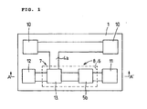
- Fig. 1 is a plan view of an L type ladder filter.
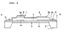
- Fig. 2 is a sectional view of a section taken along a line A-A' shown in Fig. 1.
- Fig. 3 is a circuit diagram of the L type ladder filter shown in Fig. 1.
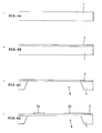
- Figs. 4A to 4D and Figs. 5A to 5D are sectional views of a key portion, showing manufacturing steps of the L type ladder filter shown in Fig. 1.
- Fig. 6 is a vertical, sectional view showing a state after a predetermined vibration portion surface is etched.
- a piezoelectric filter configured as an L type ladder filter is shown in Fig. 1 to Fig. 3.
- Reference numeral 1 denotes a silicon substrate that is susceptible to anisotropic etching
- reference numeral 2 denotes a thin film made of silicon oxide (SiO 2 ).
- reference numeral 3 denotes a piezoelectric thin film composed of a thin film layer primarily containing zinc oxide (ZnO)
- reference numerals 4a and 4b denote lower electrodes made of aluminum (Al) or other suitable material
- reference numerals 5a and 5b denote upper electrodes also made of aluminum (Al) or other suitable material.
- the substrate 1 is preferably made of a silicon wafer. This substrate 1 is provided with an opening 6 to become a vertically penetrating through hole. This opening 6 ensures a vibration space of a parallel piezoelectric resonator 7 and a series piezoelectric resonator 8 having vibration portions including a piezoelectric thin film 3, lower electrodes 4a and 4b and upper electrodes 5a and 5b.
- the thin film 2 is provided in the state of covering all over the opening 6.
- the thin film 2 is a diaphragm 9 as a support portion for supporting the parallel piezoelectric resonator 7 and the series piezoelectric resonator 8.
- the lower electrodes 4a and 4b are individually provided on the diaphragm 9.
- the lower electrode 4a is connected to a GND electrode 10.
- the lower electrode 4b is connected to an output electrode 11.
- the piezoelectric thin film 3 constituting at least one layer primarily including zinc oxide (ZnO) is provided as a thin film portion on the lower electrodes 4a and 4b.
- the upper electrode 5a is provided in order that the piezoelectric thin film 3 is vertically sandwiched between the upper electrode 5a and the lower electrode 4a in the region of the diaphragm 9 while a portion of the upper electrode 5a faces the lower electrode 4a in the vertical direction.
- the upper electrode 5b is provided in order that the piezoelectric thin film 3 is vertically sandwiched between the upper electrode 5b and the lower electrode 4b in the region of the diaphragm 9 while a portion of the upper electrode 5b faces the lower electrode 4b in the vertical direction.
- These upper electrodes 5a and 5b are formed in the same manner as the thin film layer, and the thicknesses of the electrodes 5a and 5b are differentiated from each other, as described below. Both the upper electrodes 5a and 5b are connected to an input electrode 12.
- the lower electrode 4a and the upper electrode 5a vertically overlap one another to take the shape of an approximate rectangle when viewed from the overlapping direction.
- the lower electrode 4b and the upper electrode 5b vertically overlap one another to take the shape of an approximate rectangle when viewed from the overlapping direction.
- the parallel piezoelectric resonator 7 is configured to have a vibration portion including the lower electrode 4a, the upper electrode 5a and a portion of the piezoelectric thin film 3 vertically sandwiched therebetween.
- the series piezoelectric resonator 8 is configured to have a vibration portion including the lower electrode 4b, the upper electrode 5b and a portion of the piezoelectric thin film 3 vertically sandwiched therebetween.
- the vibration mode of the vibration portion may be the thickness shear vibration.
- the upper electrode 5a and the upper electrode 5b are integrally provided as one electrode film, as described below.
- the upper electrode 5b is etched to have a thickness that is smaller than that of the upper electrode 5a.
- the reason for processing to have such a reduced thickness is that in particular, the upper electrode 5b is selectively etched in order to adjust the setting of the resonant frequency. Consequently, an etching retardant film 13 made of alumina (Al 2 O 3 ) or other suitable material is provided as a surface portion layer on the surface of the upper electrode 5a as an electrode layer.
- Alumina is less susceptible to etching compared with Al which is the material for upper electrodes 5a and 5b under the same condition.
- the resonant frequency of the piezoelectric resonator is determined based on the thickness of the vibration portion including the thin film 2, the piezoelectric thin film 3, the lower electrodes 4a and 4b, the upper electrodes 5a and 5b and the etching retardant film 13.
- the pass band width is determined based on the difference in the resonant frequency between the series piezoelectric resonator and the parallel piezoelectric resonator.
- etching for adjusting the frequencies of the parallel piezoelectric resonator 7 and the series piezoelectric resonator 8 is performed from above the parallel piezoelectric resonator 7 and the series piezoelectric resonator 8 in the condition in which the etching retardant film 13 made of alumina (Al 2 O 3 ) or other suitable material is provided as the surface portion layer on the surface of the upper electrode 5a, as in the present preferred embodiment, while alumina has susceptibility to etching lower than that of Al which is the material used for upper electrodes 5a and 5b, the etching retardant film 13 having low susceptibility to etching is hardly etched.
- alumina Al 2 O 3
- the upper electrode 5b is etched, and thereby, the thickness of the upper electrode 5b becomes smaller than that of the upper electrode 5a. That is, the thickness of the vibration portion of the series piezoelectric resonator 8 is made smaller than that of the vibration portion of the parallel piezoelectric resonator 7. As a result, the difference in resonant frequency between the series piezoelectric resonator and the parallel piezoelectric resonator is varied, and the pass band width can be adjusted to a desired value.
- the etching retardant film 13 made of a material having susceptibility to etching that is lower than that of the upper electrodes 5a and 5b, under the same condition, is provided on the surface of the upper electrode 5a, the etching proceeding rate in the parallel piezoelectric resonator 7 is differentiated from that in the series piezoelectric resonator 8, and thereby, the difference in resonant frequency between the series piezoelectric resonator and the parallel piezoelectric resonator is adjusted, and the pass band width is adjusted to a desired value.
- the etching for adjusting the frequencies of the parallel piezoelectric resonator 7 and the series piezoelectric resonator 8 is performed from above the parallel piezoelectric resonator 7 and the series piezoelectric resonator 8, so that the difference between the thicknesses of the vibration portions of the parallel piezoelectric resonator 7 and the series piezoelectric resonator 8 is adjusted, and thereby, the pass band width is adjusted to a desired value.
- an adjusting film 14 is additionally provided on the bottom side of the thin film 2, so that the frequency of the total piezoelectric filter is adjusted.
- the frequency of the total piezoelectric filter is varied depending on the thickness of the adjusting film 14 added, and the frequency of the total piezoelectric filter is lowered with an increase in thickness of the adjusting film 14.
- the thin film 2 is etched from the bottom side, and the adjustment is performed by reducing the thickness of the thin film 2.
- FIG. 4A the substrate 1 in the state of silicon wafer is prepared.
- the thin film 2 made of silicon oxide (SiO 2 ) is formed on one surface (put another way, the top surface) of the substrate 1.
- This thin film 2 is formed onto the surface of the substrate 1 by a sputtering method, a CVD method or other suitable process.
- a hollow-shaped opening 6 is formed from the other surface (put another way, the bottom surface) of the substrate 1 up to the thin film 2.
- the opening 6 is provided by anisotropic etching, reactive etching, processing with a laser or other suitable process, as necessary.
- the outline of the opening 6 viewed from the surface side of the substrate 1 is indicated by a broken line.
- an electrode film is formed all over the thin film 2 from aluminum (Al) or other suitable material as a material by vacuum evaporation, sputtering or other suitable process, while necessary regions on the surface of the thin film 2 are protected by a patterned resist film, although not shown in the drawing. Subsequently, the resist film is peeled off, and therefore, each of the lower electrodes 4a and 4b is formed. Au, Pt, Nb, W, Cu, Ag or other suitable material may be used for the lower electrodes 4a and 4b instead of Al.
- a piezoelectric thin film 3 primarily including zinc oxide (ZnO) is formed by vacuum evaporation, sputtering or other suitable process while masking is performed with a metal mask or the like, although not shown in the drawing.
- an upper electrode pattern is formed with a resist film not shown in the drawing, and an aluminum (Al) film is formed over the entire surface. Subsequently, the resist film is peeled off, so that an upper electrode portion 5 for forming the upper electrodes 5a and 5b is formed.
- the upper electrode 5a and 5b may be separately formed in order that the upper electrodes 5a and 5b have the predetermined required thicknesses, as shown in Fig. 24. In this case, the upper electrode 5a and the upper electrode 5b are electrically connected at x where no influence is exerted on the vibration.
- the etching retardant film 13 as an additional film made of alumina (Al 2 O 3 ) is formed on the top surface of the upper electrode 5a by vacuum evaporation, sputtering or other process while masking is performed with a metal mask or the like, although not shown in the drawing.
- films of a pad portion of the input electrode 12 connected to the upper electrode 5a, a pad portion of the output electrode 11 connected to the lower electrode 4b and a pad portion of the GND electrode 10 are formed.
- the GND electrode 10, the output electrode 11 and the input electrode 12 may be simultaneously formed during film formation of the electrodes.
- a piezoelectric filter in the condition antecedent to the frequency adjustment is produced through the steps up to this point.
- this piezoelectric filter With respect to the series piezoelectric resonator 8, processing for reducing the thickness thereof is performed, and thereby, the resonant frequency of the series piezoelectric resonator 8 is adjusted to become close to the desired frequency.
- a measurement apparatus e.g. a high-frequency network analyzer, may be used for this adjustment.
- a frequency signal from the high-frequency network analyzer is input between the input electrode 12 and the GND electrode 10, and thereby, a signal is output between the output electrode 11 and the GND electrode 10 in response to the input signal.
- the center frequency and the pass band width of a filter including the parallel piezoelectric resonator 7 and the series piezoelectric resonator 8 are measured with the high-frequency network analyzer.
- the amount of deviation from the desired value of the pass band width required of the piezoelectric filter is determined based on this measurement result.
- the ion milling time t 1 required for adjusting the frequency to achieve a desired pass band width can be calculated based on the relationship between the ion milling time in terms of etching in an argon (Ar) atmosphere and the amount of decrease in the pass band width of a good piezoelectric filter, the relationship being experimentally determined in advance.
- the evaporation time t 2 required for achieving the desired center frequency can be calculated based on the amount of deviation from- the desired value of the center frequency and the relationship between the evaporation time for forming the adjusting film 14 made of silver (Ag) or other suitable material and the amount of decrease in the center frequency, the relationship being experimentally determined in advance.
- Numerical values of the ion milling rates in this argon atmosphere are specifically shown below. The ion milling rates are about 2.0 (nm/min) with respect to aluminum, about 10.0 (nm/min) with respect to gold and about 0.2 (nm/min) with respect to alumina (Al 2 O 3 ).
- the above-described piezoelectric filter is introduced into an ion milling apparatus, and the surface is etched in the argon atmosphere just for a time t 1 based on the above-described calculation result.
- the upper electrodes 5a and 5b since the upper electrode 5b is more susceptible to etching compared with the upper electrode 5a provided with the etching retardant film 13, reduction in thickness of the upper electrode 5b is accelerated by this etching. Consequently, the resonant frequency of the series piezoelectric resonator 8 is adjusted to shift to the higher side.
- the difference in resonant frequency between the series piezoelectric resonator and the parallel piezoelectric resonator can be thereby adjusted, and the pass band width can be adjusted to a desired value.
- the resulting piezoelectric filter is introduced into an evaporation apparatus, silver (Ag) is evaporated onto the bottom surface of the diaphragm 9 just for a time t 2 to form the adjusting film 14, and thereby, the frequency of the total piezoelectric filter is adjusted. In this manner, both the pass band width and the center frequency of the piezoelectric filter are adjusted at desired values.
- An insulating film made of SiO 2 or other suitable material may be used in place of silver (Ag).
- the L type ladder filter having an adjusted frequency can be produced, as shown in Fig. 1.
- the resonant frequencies of the series piezoelectric resonator and the parallel piezoelectric resonator constituting this piezoelectric filter can be simultaneously adjusted.
- a mask or the like is required for a vibration portion not targeted for the adjustment.
- simplification of the adjustment steps can be achieved.
- the frequencies of a plurality of filter elements provided on the substrate can be adjusted by one operation.
- the etching retardant film is formed on the upper electrode of one of the series piezoelectric resonator and the parallel piezoelectric resonator, while the etching retardant film has susceptibility to etching that is lower than that of the upper electrode material under the same condition.
- the degree of change in frequency due to etching of the series piezoelectric resonator is thereby differentiated from that of the parallel piezoelectric resonator.
- the difference in resonant frequency between the series piezoelectric resonator and the parallel piezoelectric resonator is adjusted by etching of the upper electrode without using a mask and the like, and therefore, the pass band width of the piezoelectric filter can be adjusted to a desired value.
- the total piezoelectric filter can be adjusted by etching of the thin film provided to block the opening or by addition of the adjusting film to the thin film, each performed from the opening side.
- the frequency of the total filter may be adjusted as a first step, and thereafter, the frequency of each of the resonators in the series side and the parallel side may be adjusted.
- the thicknesses of the piezoelectric thin film 3 and the lower electrodes 4a and 4b are equalized, and thereafter, the thicknesses of the upper electrodes 5a and 5b are differentiated from each other, so that the resonant frequencies of the parallel piezoelectric resonator 7 and the series piezoelectric resonator 8 are differentiated from each other.
- the resonant frequencies of the parallel piezoelectric resonator 7 and the series piezoelectric resonator 8 can be adjusted simply by adjusting the thicknesses of the upper electrodes 5a and 5b.
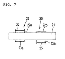
- Fig. 7 is a vertical, sectional view of the piezoelectric filter.
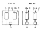
- Figs. 8A and 8B are a plan view and a bottom view, respectively, of the piezoelectric filter shown in Fig. 7.
- Fig. 9 is a circuit diagram of the piezoelectric filter shown in Fig. 7.
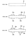
- Figs. 10A to 10C are sectional views of the key portion, illustrating manufacturing steps of the ladder filter shown in Fig. 7.
- reference numeral 21 denotes a piezoelectric substrate including a thin-plate shaped piezoelectric material preferably formed from lithium tantalate (LiTaO 3 ), reference numerals 22a and 22b denote upper electrodes made of metal films provided at the respective predetermined positions on the top surface of the substrate 21, reference numerals 23a and 23b denote lower electrodes made of metal films provided at the respective predetermined positions on the bottom surface of the substrate 21, reference numeral 24 denotes an etching retardant film as an additional film further provided on the surface of the upper electrode 22a, and reference numeral 25 denotes an etching retardant film as an additional film further provided on the surface of the lower electrode 23b.
- lithium niobate (LiNbO 3 ) quartz or other suitable material may be used for the substrate 21.
- Both the top and bottom surfaces of the substrate 21 are mirror-finished.
- a pair of upper electrodes 22a and 22b are films provided at two respective predetermined positions on the top surface of this substrate 21.
- Each of the upper electrodes 22a and 22b preferably is configured in the shape of an approximate rectangle in the plan view.
- Both the upper electrodes 22a and 22b are preferably made of aluminum (Al).
- Both the upper electrodes 22a and 22b may be formed from a high conductivity material, e.g. gold (Au), in place of aluminum.
- An etching retardant film 24 made of alumina (Al 2 O 3 ) or other suitable material is provided on the surface of one upper electrode 22a.
- Alumina has susceptibility to etching lower than that of aluminum under the same condition.
- the surface portion of the other upper electrode 22b remains in its state as formed from aluminum.
- the lower electrodes 23a and 23b are films provided on the bottom surface of the substrate 21 at the positions facing the upper electrodes 22a and 22b respectively.
- the lower electrodes 23a and 23b have the shapes of approximate rectangles, in the plan view, in accordance with the respective shapes of the upper electrodes 22a and 22b.
- Both the lower electrodes 23a and 23b are preferably made of aluminum.
- Both the lower electrodes 23a and 23b may be formed from a high conductivity material, e.g. gold (Au), in place of aluminum.
- An etching retardant film 25 made of alumina (Al 2 O 3 ) or other suitable material is provided on the surface of one lower electrode 23b.
- Alumina has a susceptibility to etching that is lower than that of aluminum under the same condition.
- the surface portion of the other lower electrode 23a remains in its state as formed from aluminum.
- a lead electrode 26 connected to both the upper electrodes 22a and 22b is provided as an input electrode on the top surface of the substrate 21.
- a lead electrode 27 connected to the lower electrode 23a is provided as a GND electrode on the bottom surface of the substrate 21.
- a lead electrode 28 connected to the lower electrode 23b is provided as an output electrode on the bottom surface of the substrate 21.
- the parallel piezoelectric resonator 29 is configured to have a vibration portion including the lower electrode 23a, the upper electrode 22a and a portion of the substrate 21 vertically sandwiched therebetween.
- the series piezoelectric resonator 30 is configured to have a vibration portion including the lower electrode 23b, the upper electrode 22b and a portion of the substrate 21 vertically sandwiched therebetween. In this manner, an L type ladder piezoelectric filter shown in Fig. 9 is configured.
- the substrate 21 preferably made lithium tantalate (LiTaO 3 ) in the shape of a thin plate with both surfaces mirror-finished is prepared.
- electrode films are formed all over the substrate 21 from aluminum (Al) or other suitable material as a material by vacuum evaporation, sputtering or other suitable process, while necessary regions on both surfaces of the substrate 21 are individually protected by patterned resist films, although not shown in the drawing. Subsequently, the resist films are peeled off, and therefore, each of the upper electrodes 22a and 22b and the lower electrodes 23a and 23b is formed.
- etching retardant films 24 and 25 made of alumina (Al 2 O 3 ) are formed in accordance with the portions on which the upper electrode 22a and the lower electrode 23b are provided, by vacuum evaporation, sputtering or other suitable process while masking is performed with a metal mask or the like, although not shown in the drawing.
- Lead electrodes 26, 27 and 28 and the like are formed on the substrate 21.
- the lead electrodes 26, 27 and 28 may be integrally formed with the upper electrodes 22a and 22b and the lower electrodes 23a and 23b.
- a piezoelectric filter in the condition antecedent to the frequency adjustment is produced through the steps up to this point.
- this piezoelectric filter With respect to each of the parallel piezoelectric resonator 29 and the series piezoelectric resonator 30, processing for reducing the thickness thereof is individually performed, and thereby, the resonant frequency of each of the resonators 29 and 30 is adjusted at the desired frequency.
- a measurement apparatus e.g. a high-frequency network analyzer, is used for this adjustment.
- a frequency signal from the high-frequency network analyzer is input between the lead electrode 26 and the lead electrode 27, and thereby, the vibration portion located therebetween is excited.
- the resonant frequency of the parallel piezoelectric resonator 29 is measured based on the reflection characteristic at that time.
- a signal is input between the lead electrode 26 and the lead electrode 28, and the resonant frequency of the series piezoelectric resonator 30 is measured based on the reflection characteristic thereof.
- the amount of deviation from the desired frequency of each of the parallel piezoelectric resonator 29 and the series piezoelectric resonator 30 can be determined based on the measurement results.
- the ion milling time required for adjustment to achieve a desired resonant frequency can be thereby determined based on the relationship between the ion milling time in terms of etching in an argon (Ar) atmosphere and the amount of deviation of the frequency, the relationship being experimentally determined in advance.
- the ion milling time required for adjusting the parallel piezoelectric resonator 29 at a desired resonant frequency is determined to be t 1
- the ion milling time required for adjusting the series piezoelectric resonator 30 at a desired resonant frequency is determined to be t 2 .
- Ion milling of the entire top surface is performed just for a time t 2 , and thereby, the upper electrode 22b is etched to an extent larger than that of the upper electrode 22a, so that the series piezoelectric resonator 30 is adjusted at the desired frequency.
- the resonant frequency of the parallel piezoelectric resonator 29 is hardly varied because the surface portion of the upper electrode 22a of the parallel piezoelectric resonator 29 is covered with the etching retardant film 24.
- ion milling of the entire bottom surface is performed just for a time t 1 , and thereby, the lower electrode 23a is etched, so that the parallel piezoelectric resonator 29 is adjusted at the desired frequency.
- the resonant frequency of the series piezoelectric resonator 30 is hardly varied because the surface portion of the lower electrode 23b of the series piezoelectric resonator 30 is covered with the etching retardant film 25.
- each of the series piezoelectric resonator 30 and the parallel piezoelectric resonator 29 constituting the piezoelectric filter can be individually subjected to the frequency adjustment. Since the frequency adjustment can be separately performed with respect to the top surface and the bottom surface, the series piezoelectric resonator 30 and the parallel piezoelectric resonator 29 can be simultaneously adjusted by respective, arbitrary amounts. Since, the adjustment can be performed in a wafer state, filter elements on the wafer can be subjected to the frequency adjustment by one operation.
- the etching retardant film 24 is provided on the upper electrode 22a of the parallel piezoelectric resonator 29, and thereby, the etching rate of the upper electrode 22a is differentiated from that of the upper electrode 22b of the series piezoelectric resonator 30, although not limited to this.
- the electrode material for the upper electrode 22a of the parallel piezoelectric resonator 29 may have an etching rate different from that of the electrode material for the upper electrode 22b of the series piezoelectric resonator 30.
- the etching retardant film 25 is provided on the lower electrode 23b of the series piezoelectric resonator 30, and thereby, the etching rate of the lower electrode 23b is differentiated from that of the lower electrode 23a of the parallel piezoelectric resonator 29, although it is not limited to this.
- the electrode material for the lower electrode 23b of the series piezoelectric resonator 30 may have an etching rate different from that of the electrode material for the lower electrode 23a of the parallel piezoelectric resonator 29.
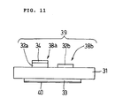
- Fig. 11 is a vertical, sectional view of the piezoelectric filter.
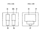
- Figs. 12A and 12B are a plan view and a bottom view, respectively, of the piezoelectric filter shown in Fig. 11.
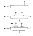
- Figs. 13A to 13C are sectional views of the key portion, illustrating manufacturing steps of the piezoelectric filter shown in Fig. 11.
- FIG. 11 A piezoelectric filter constituting a double-mode filter is shown in Fig. 11.
- reference numeral 31 denotes a piezoelectric substrate preferably made of a thin-plate shaped piezoelectric material formed from lithium tantalate (LiTaO 3 )
- reference numerals 32a and 32b denote upper electrodes made of metal films provided at the respective predetermined positions on the top surface of the substrate 31
- reference numerals 33 denotes a lower electrode made of a metal film formed at the predetermined position on the bottom surface of the substrate 31
- reference numeral 34 denotes an etching retardant film further provided on the surface of the upper electrode 32a.
- lithium niobate (LiNbO 3 ) quartz or other suitable material may be used for the substrate 31.
- Both the top and bottom surfaces of the substrate 31 are preferably mirror-finished.
- a pair of upper electrodes 32a and 32b are films provided at two respective predetermined positions on the top surface of this substrate 31.
- Each of the upper electrodes 32a and 32b preferably has the configuration of an approximate rectangle in the plan view.
- Both the upper electrodes 32a and 32b are preferably made of aluminum (Al).
- Both the upper electrodes 32a and 32b may be formed from a high conductivity material, e.g. gold (Au), in place of aluminum.
- An etching retardant film 34 made of alumina (Al 2 O 3 ) or other suitable material is provided as an additional film on the surface of one upper electrode 32a.
- Alumina has susceptibility to etching lower than that of aluminum under the same condition.
- the surface portion of the other upper electrode 32b remains in its state as formed from aluminum.
- a film of lower electrode 33 having the shape of an approximate rectangle, in the plan view, is provided on the bottom surface of the substrate 31 at the position facing both the upper electrodes 32a and 32b.
- the lower electrode 33 is preferably made of aluminum.
- the lower electrode 33 may be formed from a high conductivity material, e.g. gold (Au), in place of aluminum.
- the lower electrode 33 is provided with an adjusting film 40 by lamination, while the adjusting film 40 has been subjected to the frequency adjustment, as described below.
- a lead electrode 35 connected to the upper electrode 32a is provided as an input electrode on the top surface of the substrate 31.
- a lead electrode 36 connected to the upper electrode 32b is provided as an output electrode on the top surface of the substrate 31.
- a lead electrode 37 connected to the lower electrode 33 is provided as a GND electrode on the bottom surface of the substrate 31.
- the vibration portion 38a of the piezoelectric resonator includes the lower electrode 33, the upper electrode 32a and a portion of the substrate 31 vertically sandwiched therebetween.
- the vibration portion 38b of the piezoelectric resonator includes the lower electrode 33, the upper electrode 32b and a portion of the substrate 31 vertically sandwiched therebetween.
- the piezoelectric filter 39 is configured by the interaction of the vibration portions 38a and 38b of the piezoelectric resonators.
- the substrate 31 preferably made of lithium tantalate (LiTaO 3 ) in the shape of a thin plate with both surfaces mirror-finished is prepared.
- electrode films are formed all over the substrate 31 from aluminum (Al) or other suitable material as a material by vacuum evaporation, sputtering or other suitable process, while necessary regions on both surfaces of the substrate 31 are individually protected by patterned resist films, although not shown in the drawing. Subsequently, the resist films are peeled off, and therefore, each of the upper electrodes 32a and 32b and the lower electrode 33 is formed.
- an etching retardant film 34 made of alumina (Al 2 O 3 ) is formed in accordance with the portion on which the upper electrode 32a is provided, by vacuum evaporation, sputtering or other suitable process while masking is performed with a metal mask or the like, although not shown in the drawing.
- Lead electrodes 35, 36 and 37 and the like are films provided on the substrate 31.
- a piezoelectric filter 39 in the condition antecedent to the frequency adjustment is produced through the steps up to this point.
- the piezoelectric filter 39 in the condition antecedent to the frequency adjustment is placed in an etching apparatus.
- This etching apparatus is provided with a measurement apparatus for measuring the pass band and the center frequency of the piezoelectric filter.
- the pass band width and the center frequency of the piezoelectric filter 39 are measured while a high-frequency probe is in contact with the lead electrode 35 as an input terminal, the lead electrode 36 as an output terminal and the lead electrode 37 as a GND terminal.
- An etching treatment to reduce the film thickness of the vibration portions 38a and 38b of the piezoelectric resonator is performed with the etching apparatus based on the measurement results, so that the frequencies are adjusted.
- the ion milling of the upper electrodes 32a and 32b on the top surface of the substrate 31 is performed while the pass band width is measured.
- the upper electrode 32b is more susceptible to the milling compared with the upper electrode 32a provided with the etching retardant film 34, the resonant frequencies in the oblique symmetric mode and the symmetric mode deviate from each other. Consequently, the pass band width is decreased.
- the processing is performed until the desired pass band width is achieved.
- an adjusting film 40 is formed by an evaporation treatment of, e.g. silver onto the lower electrode 33 on the bottom surface of the substrate 31.
- the center frequency of the piezoelectric filter 39 is shifted to the lower frequency side due to an effect of the addition of mass through this evaporation.
- the evaporation treatment is performed until the desired center frequency is achieved.
- the double-mode filter having this structure is adjusted at a desired resonant frequency.
- the pass band width can be adjusted by etching of the upper electrode on the top surface of the substrate 31, and the center frequency can be adjusted by addition of a film to the lower electrode on the bottom surface of the substrate 31. Since the filter characteristic can be adjusted while the vibration portion is directly subjected to the measurement, the adjustment can be performed with high accuracy.
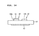
- Fig. 14 is a vertical, sectional view of the piezoelectric filter.
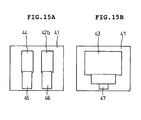
- Figs. 15A and 15B are a plan view and a bottom view, respectively, of the piezoelectric filter shown in Fig. 14.
- Figs. 16A to 16C are sectional views of the key portion, illustrating manufacturing steps of the piezoelectric filter shown in Fig. 14.
- Fig. 14 shows a ladder piezoelectric filter including one series resonator and one parallel resonator.
- reference numeral 41 denotes a piezoelectric substrate preferably made of a thin-plate shaped piezoelectric material formed from lithium tantalate (LiTaO 3 )
- reference numerals 42a and 42b denote upper electrodes made of metal films provided at the respective predetermined positions on the top surface of the substrate 41
- reference numerals 43 denotes a lower electrode made of a metal film formed at the predetermined position on the bottom surface of the substrate 41
- reference numeral 44 denotes an easy-to-etch film further provided on the surface of the upper electrode 42a.
- lithium niobate (LiNbO 3 ) quartz or other suitable material may be used for the substrate 41.
- Both the top and bottom surfaces of the substrate 41 are preferably mirror-finished.
- a pair of upper electrodes 42a and 42b are films provided at two respective predetermined positions on the top surface of this substrate 41. Each of the upper electrodes 42a and 42b is in the shape of an approximate rectangle in the plan view. Both the upper electrodes 42a and 42b are preferably made of aluminum (Al).
- An easy-to-etch film 44 made of gold (Au) or other suitable material is provided as an additional film on the surface of one upper electrode 42a. Gold has susceptibility to etching higher than that of aluminum under the same condition, and therefore, etching proceeds at a high rate.
- the surface portion of the other upper electrode 42b remains in its state as formed from aluminum.
- the lower electrode 43 is preferably made of aluminum.
- the lower electrode 43 may be formed from a high conductivity material, e.g. gold (Au), in place of aluminum.
- Au gold
- the lower electrode 43 has been subjected to etching in order to adjust the frequency, as described below.
- a lead electrode 45 connected to the upper electrode 42a is provided as a GND electrode on the top surface of the substrate 41.
- a lead electrode 46 connected to the upper electrode 42b is provided as an output electrode on the top surface of the substrate 41.
- a lead electrode 47 connected to the lower electrode 43 is provided as an input electrode on the bottom surface of the substrate 41.
- the piezoelectric resonator 48 is configured to have a vibration portion including the lower electrode 43, the upper electrode 42a and a portion of the substrate 41 vertically sandwiched therebetween.
- the piezoelectric resonator 49 is configured to have a vibration portion including the lower electrode 43, the upper electrode 42b and a portion of the substrate 41 vertically sandwiched therebetween.
- the substrate 41 preferably made of lithium tantalate (LiTaO 3 ) in the shape of a thin plate with both surfaces mirror-finished is prepared.
- electrode films are formed all over the substrate 41 from aluminum (Al) or other suitable material as a material by vacuum evaporation, sputtering or other suitable process, while necessary regions on both surfaces of the substrate 41 are individually protected by patterned resist films, although not shown in the drawing. Subsequently, the resist films are peeled off, and therefore, each of the upper electrodes 42a and 42b and the lower electrode 43 is formed.
- an easy-to-etch film 44 made of gold (Au) is formed in accordance with the portion on which the upper electrode 42a is provided, by vacuum evaporation, sputtering or other suitable process while masking is performed with a metal mask or the like, although not shown in the drawing.
- Films of lead electrodes 45, 46 and 47 and the like are formed on the substrate 41.
- a piezoelectric filter in the condition antecedent to the frequency adjustment is produced through the steps up to this point.
- the frequency adjustment of this piezoelectric filter will be described.
- processing for reducing the thickness thereof is individually performed, and thereby, the resonant frequency of each of the piezoelectric resonators 48 and 49 is adjusted at the desired frequency.
- a measurement apparatus e.g. a high-frequency network analyzer
- a frequency signal from the high-frequency network analyzer is input between the lead electrode 45 and the lead electrode 47, and thereby, the vibration portion located therebetween is excited, so that the resonant frequency of the piezoelectric resonator 48 is measured.
- a frequency signal from the high-frequency network analyzer is input between the lead electrode 46 and the lead electrode 47, and thereby, the vibration portion located therebetween is excited, so that the resonant frequency of the piezoelectric resonator 49 is measured.
- the amount of deviation from the desired frequency of each of the piezoelectric resonators 48 and 49 can be determined based on the measurement results.
- the ion milling time required for adjustment to achieve a desired resonant frequency can be thereby determined based on the relationship between the ion milling time in terms of etching in an argon (Ar) atmosphere and the amount of deviation of the frequency, the relationship being experimentally determined in advance. It is assumed that the ion milling time required for adjusting the piezoelectric resonator 48 at a desired resonant frequency is determined to be t 1 , and the ion milling time required for adjusting the piezoelectric resonator 49 at a desired resonant frequency is determined to be t 2 .
- Ion milling of the entire top surface is performed just for a time t 1 , and thereby, the easy-to-etch film 44 provided on the upper electrode 42a is etched to a greater extent than that of the upper electrode 42b, so that the resonant frequency of the piezoelectric resonator 48 is shifted to the higher side, and is adjusted at the desired frequency.
- the resonant frequency of this piezoelectric resonator 48 is shifted more than the resonant frequency of the piezoelectric resonator 49. In this manner, the pass band width can be adjusted to a desired value.
- ion milling of the entire bottom surface is performed just for a time t 2 , and thereby, the lower electrode 43 is etched. Consequently, the center frequency of the piezoelectric filter can be adjusted.
- a duplexer according to a preferred embodiment of the present invention will be described.
- a duplexer 50 shown in Fig. 17 is provided with an antenna terminal 51, a receiving-side terminal 52 and a transmitting-side terminal 53.
- piezoelectric filters according to other preferred embodiments of the present invention are provided between the receiving-side terminal 52 and the antenna terminal 51, and between the transmitting-side terminal 53 and the antenna terminal 51, while the piezoelectric filters simply permit passing of signals within a desired frequency band.
- FIG. 18 is a simplified block diagram of the communication device.
- the main body of this communication device 54 is provided with a receiving circuit 55, a transmitting circuit 56 and an antenna 57, as shown in Fig. 18. Signals are transmitted between the antenna 57 and the transmitting circuit 56 and between the antenna 57 and the receiving circuit 55 via the duplexer 50 described above in the fifth preferred embodiment.
- This duplexer 50 includes the piezoelectric filter according to a preferred embodiment of the present invention as a circuit element, and thereby, the operating characteristics of this communication device are stabilized.
- Fig. 19 is a vertical, sectional view of a piezoelectric filter.
- Figs. 20A and 20B are a plan view and a bottom view, respectively, of the piezoelectric filter shown in Fig. 19.
- films of a pair of upper electrodes 62a and 62b are provided on the top surface side of a piezoelectric substrate 61 which is preferably made of a thin-plate shaped piezoelectric material.
- a film defining a lower electrode 63 is provided on the bottom surface side of the substrate 61 to face each of the upper electrodes 62a and 62b.
- a lead electrode 64 connected to the upper electrode 62a is provided as a GND electrode on the top surface of the substrate 61.
- a lead electrode 65 connected to the upper electrode 62b is provided as an output electrode on the top surface of the substrate 61.
- a lead electrode 66 connected to the lower electrode 63 is provided as an input electrode on the bottom surface of the substrate 61.
- the parallel piezoelectric resonator 67 is provided to have a vibration portion including the upper electrode 62a, the lower electrode 63 and a portion of the substrate 61 sandwiched between both electrodes 62a and 63.
- the series piezoelectric resonator 68 is provided to have a vibration portion including the upper electrode 62b, the lower electrode 63 and a portion of the substrate 61 sandwiched between both the electrodes 62b and 63.
- the upper electrode 62a is a film preferably formed from gold (Au).
- the upper electrode 62a and the lower electrode 63 are films preferably formed from aluminum (Al). Consequently, the upper electrode 62a is more susceptible to etching compared with the upper electrode 62b under the same condition.
- a frequency signal from the high-frequency network analyzer is input between the input electrode 66 and the electrode 65, and thereby, the vibration portion located therebetween is excited, so that the resonant frequency of the series piezoelectric resonator 68 is measured.
- the amount of deviation from the desired frequency of each of the parallel piezoelectric resonator 67 and the series piezoelectric resonator 68 can be determined based on the measurement results.
- the ion milling time required for adjustment to achieve a desired resonant frequency can be thereby determined based on the relationship between the ion milling time in terms of etching in an argon (Ar) atmosphere and the amount of deviation of the frequency, the relationship being experimentally determined in advance.
- the ion milling time required for adjusting the parallel piezoelectric resonator 67 to a desired resonant frequency is determined to be t 1
- the ion milling time required for adjusting the series piezoelectric resonator 68 to a desired resonant frequency is determined to be t 2 .
- Ion milling of the entire top surface is performed just for a time t 1 , and thereby, the upper electrode 62a is etched to an extent larger than that of the upper electrode 62b, so that the resonant frequency of the piezoelectric resonator 67 is shifted to the higher side, and is adjusted at the desired frequency.
- the upper electrode 62a of the piezoelectric resonator 67 is more susceptible to etching compared with the upper electrode 62b, the resonant frequency of this piezoelectric resonator 67 is shifted larger than the resonant frequency of the piezoelectric resonator 68.
- the pass band width of the piezoelectric filter can be adjusted to a desired value.
- ion milling of the entire bottom surface is performed just for a time t 2 , and thereby, the lower electrode 63 is etched. Consequently, the center frequency of the piezoelectric filter can be adjusted.
- the present invention is not limited to that described above in each of the various preferred embodiments.
- the present invention may include, for example, the following modifications and applications.
- Two upper electrodes made of metal films arranged at respective predetermined positions are provided on the top surface of a piezoelectric substrate preferably made of a thin-plate shaped piezoelectric material formed from lithium tantalate (LiTaO 3 ).
- a lower electrode facing each of the upper electrodes with the piezoelectric substrate therebetween in the thickness direction is provided on the bottom surface of this piezoelectric substrate.
- a piezoelectric resonator is configured to include a vibration portion including each of the upper electrode and lower electrode facing each other and a portion of the piezoelectric substrate sandwiched between those electrodes.
- a protective film made of aluminum (Al) or other suitable material is arranged to cover at least the entire upper electrodes of the vibration portions of both the piezoelectric resonators and a portion of the top surface of the piezoelectric substrate between the two vibration portions. Furthermore, a film of additional electrode made of gold (Au) or other suitable material is laminated on the protective film surface of one upper electrode.
- the protective film has electrical conductivity, and there is electrical continuity between the additional electrode and the upper electrode via the protective film.
- the protective film and the additional electrode have different etching rates under the same condition.
- the protective film and the additional electrode are films formed to have predetermined thicknesses. For example, lithium niobate (LiNbO 3 ), quartz or other suitable material may be used for the piezoelectric substrate.
- the frequency of the vibration portion can be adjusted in a manner similar to that in the above-described preferred embodiments of each piezoelectric filter.
Landscapes
- Engineering & Computer Science (AREA)
- Manufacturing & Machinery (AREA)
- Chemical & Material Sciences (AREA)
- Crystallography & Structural Chemistry (AREA)
- Physics & Mathematics (AREA)
- Acoustics & Sound (AREA)
- Piezo-Electric Or Mechanical Vibrators, Or Delay Or Filter Circuits (AREA)
Applications Claiming Priority (4)
| Application Number | Priority Date | Filing Date | Title |
|---|---|---|---|
| JP2002213773 | 2002-07-23 | ||
| JP2002213773 | 2002-07-23 | ||
| JP2003175235 | 2003-06-19 | ||
| JP2003175235A JP4039322B2 (ja) | 2002-07-23 | 2003-06-19 | 圧電フィルタ、デュプレクサ、複合圧電共振器および通信装置、並びに、圧電フィルタの周波数調整方法 |
Publications (2)
| Publication Number | Publication Date |
|---|---|
| EP1385265A2 true EP1385265A2 (fr) | 2004-01-28 |
| EP1385265A3 EP1385265A3 (fr) | 2005-05-11 |
Family
ID=30002382
Family Applications (1)
| Application Number | Title | Priority Date | Filing Date |
|---|---|---|---|
| EP20030016796 Withdrawn EP1385265A3 (fr) | 2002-07-23 | 2003-07-23 | Filtre piézoélectrique, duplexeur, résonateur piézoélectrique composite, dispositif de communication et procédé de réglage du filtre piézoélectrique |
Country Status (3)
| Country | Link |
|---|---|
| US (1) | US7019604B2 (fr) |
| EP (1) | EP1385265A3 (fr) |
| JP (1) | JP4039322B2 (fr) |
Cited By (1)
| Publication number | Priority date | Publication date | Assignee | Title |
|---|---|---|---|---|
| WO2007000929A1 (fr) * | 2005-06-29 | 2007-01-04 | Matsushita Electric Industrial Co., Ltd. | Resonateur et filtre piezoelectriques, resonateur et dispositif de communication l'utilisant |
Families Citing this family (74)
| Publication number | Priority date | Publication date | Assignee | Title |
|---|---|---|---|---|
| US7275292B2 (en) | 2003-03-07 | 2007-10-02 | Avago Technologies Wireless Ip (Singapore) Pte. Ltd. | Method for fabricating an acoustical resonator on a substrate |
| US7332985B2 (en) * | 2003-10-30 | 2008-02-19 | Avago Technologies Wireless Ip (Singapore) Pte Ltd. | Cavity-less film bulk acoustic resonator (FBAR) devices |
| EP1528677B1 (fr) | 2003-10-30 | 2006-05-10 | Agilent Technologies, Inc. | Transformateur à couplage acoustique de couches minces avec deux éléments piézoélectriques à axe-c inversé |
| US6946928B2 (en) * | 2003-10-30 | 2005-09-20 | Agilent Technologies, Inc. | Thin-film acoustically-coupled transformer |
| US7362198B2 (en) * | 2003-10-30 | 2008-04-22 | Avago Technologies Wireless Ip (Singapore) Pte. Ltd | Pass bandwidth control in decoupled stacked bulk acoustic resonator devices |
| US7019605B2 (en) * | 2003-10-30 | 2006-03-28 | Larson Iii John D | Stacked bulk acoustic resonator band-pass filter with controllable pass bandwidth |
| US7531943B2 (en) * | 2004-03-31 | 2009-05-12 | Panasonic Corporation | Acoustic resonator and filter |
| JP4373949B2 (ja) * | 2004-04-20 | 2009-11-25 | 株式会社東芝 | 薄膜圧電共振器及びその製造方法 |
| US20060006965A1 (en) * | 2004-07-06 | 2006-01-12 | Matsushita Electric Industrial Co., Ltd. | RF filter and method for fabricating the same |
| US7615833B2 (en) | 2004-07-13 | 2009-11-10 | Avago Technologies Wireless Ip (Singapore) Pte. Ltd. | Film bulk acoustic resonator package and method of fabricating same |
| US7388454B2 (en) * | 2004-10-01 | 2008-06-17 | Avago Technologies Wireless Ip Pte Ltd | Acoustic resonator performance enhancement using alternating frame structure |
| US8981876B2 (en) * | 2004-11-15 | 2015-03-17 | Avago Technologies General Ip (Singapore) Pte. Ltd. | Piezoelectric resonator structures and electrical filters having frame elements |
| US7202560B2 (en) | 2004-12-15 | 2007-04-10 | Avago Technologies Wireless Ip (Singapore) Pte. Ltd. | Wafer bonding of micro-electro mechanical systems to active circuitry |
| US7791434B2 (en) * | 2004-12-22 | 2010-09-07 | Avago Technologies Wireless Ip (Singapore) Pte. Ltd. | Acoustic resonator performance enhancement using selective metal etch and having a trench in the piezoelectric |
| US7427819B2 (en) * | 2005-03-04 | 2008-09-23 | Avago Wireless Ip Pte Ltd | Film-bulk acoustic wave resonator with motion plate and method |
| US7369013B2 (en) * | 2005-04-06 | 2008-05-06 | Avago Technologies Wireless Ip Pte Ltd | Acoustic resonator performance enhancement using filled recessed region |
| US7436269B2 (en) | 2005-04-18 | 2008-10-14 | Avago Technologies Wireless Ip (Singapore) Pte. Ltd. | Acoustically coupled resonators and method of making the same |
| US7868522B2 (en) | 2005-09-09 | 2011-01-11 | Avago Technologies Wireless Ip (Singapore) Pte. Ltd. | Adjusted frequency temperature coefficient resonator |
| US7391286B2 (en) * | 2005-10-06 | 2008-06-24 | Avago Wireless Ip Pte Ltd | Impedance matching and parasitic capacitor resonance of FBAR resonators and coupled filters |
| US7675390B2 (en) * | 2005-10-18 | 2010-03-09 | Avago Technologies Wireless Ip (Singapore) Pte. Ltd. | Acoustic galvanic isolator incorporating single decoupled stacked bulk acoustic resonator |
| US7525398B2 (en) * | 2005-10-18 | 2009-04-28 | Avago Technologies General Ip (Singapore) Pte. Ltd. | Acoustically communicating data signals across an electrical isolation barrier |
| US7737807B2 (en) | 2005-10-18 | 2010-06-15 | Avago Technologies Wireless Ip (Singapore) Pte. Ltd. | Acoustic galvanic isolator incorporating series-connected decoupled stacked bulk acoustic resonators |
| US7423503B2 (en) * | 2005-10-18 | 2008-09-09 | Avago Technologies Wireless Ip (Singapore) Pte. Ltd. | Acoustic galvanic isolator incorporating film acoustically-coupled transformer |
| US7425787B2 (en) | 2005-10-18 | 2008-09-16 | Avago Technologies Wireless Ip (Singapore) Pte. Ltd. | Acoustic galvanic isolator incorporating single insulated decoupled stacked bulk acoustic resonator with acoustically-resonant electrical insulator |
| US7463499B2 (en) * | 2005-10-31 | 2008-12-09 | Avago Technologies General Ip (Singapore) Pte Ltd. | AC-DC power converter |
| US7561009B2 (en) * | 2005-11-30 | 2009-07-14 | Avago Technologies General Ip (Singapore) Pte. Ltd. | Film bulk acoustic resonator (FBAR) devices with temperature compensation |
| JP4791181B2 (ja) * | 2005-12-28 | 2011-10-12 | 京セラ株式会社 | 薄膜バルク音響波共振子、それを備えるフィルタおよび通信装置ならびに薄膜バルク音響波共振子の製造方法 |
| US7612636B2 (en) * | 2006-01-30 | 2009-11-03 | Avago Technologies Wireless Ip (Singapore) Pte. Ltd. | Impedance transforming bulk acoustic wave baluns |
| US7746677B2 (en) * | 2006-03-09 | 2010-06-29 | Avago Technologies Wireless Ip (Singapore) Pte. Ltd. | AC-DC converter circuit and power supply |
| US20070210724A1 (en) * | 2006-03-09 | 2007-09-13 | Mark Unkrich | Power adapter and DC-DC converter having acoustic transformer |
| US7479685B2 (en) * | 2006-03-10 | 2009-01-20 | Avago Technologies General Ip (Singapore) Pte. Ltd. | Electronic device on substrate with cavity and mitigated parasitic leakage path |
| US7629865B2 (en) | 2006-05-31 | 2009-12-08 | Avago Technologies Wireless Ip (Singapore) Pte. Ltd. | Piezoelectric resonator structures and electrical filters |
| US7508286B2 (en) * | 2006-09-28 | 2009-03-24 | Avago Technologies Wireless Ip (Singapore) Pte. Ltd. | HBAR oscillator and method of manufacture |
| JP4968900B2 (ja) * | 2006-10-17 | 2012-07-04 | 太陽誘電株式会社 | ラダー型フィルタの製造方法 |
| JP4838093B2 (ja) * | 2006-10-25 | 2011-12-14 | 太陽誘電株式会社 | 圧電薄膜共振器およびフィルタ |
| US20080202239A1 (en) * | 2007-02-28 | 2008-08-28 | Fazzio R Shane | Piezoelectric acceleration sensor |
| US7851333B2 (en) * | 2007-03-15 | 2010-12-14 | Infineon Technologies Ag | Apparatus comprising a device and method for producing it |
| US7791435B2 (en) * | 2007-09-28 | 2010-09-07 | Avago Technologies Wireless Ip (Singapore) Pte. Ltd. | Single stack coupled resonators having differential output |
| JP5054491B2 (ja) | 2007-11-21 | 2012-10-24 | パナソニック株式会社 | 圧電振動子およびその製造方法 |
| US7855618B2 (en) * | 2008-04-30 | 2010-12-21 | Avago Technologies Wireless Ip (Singapore) Pte. Ltd. | Bulk acoustic resonator electrical impedance transformers |
| US7732977B2 (en) * | 2008-04-30 | 2010-06-08 | Avago Technologies Wireless Ip (Singapore) | Transceiver circuit for film bulk acoustic resonator (FBAR) transducers |
| US8291559B2 (en) * | 2009-02-24 | 2012-10-23 | Epcos Ag | Process for adapting resonance frequency of a BAW resonator |
| US8248185B2 (en) * | 2009-06-24 | 2012-08-21 | Avago Technologies Wireless Ip (Singapore) Pte. Ltd. | Acoustic resonator structure comprising a bridge |
| US8902023B2 (en) * | 2009-06-24 | 2014-12-02 | Avago Technologies General Ip (Singapore) Pte. Ltd. | Acoustic resonator structure having an electrode with a cantilevered portion |
| JP2011041136A (ja) * | 2009-08-17 | 2011-02-24 | Taiyo Yuden Co Ltd | 弾性波デバイスおよびその製造方法 |
| US8193877B2 (en) * | 2009-11-30 | 2012-06-05 | Avago Technologies Wireless Ip (Singapore) Pte. Ltd. | Duplexer with negative phase shifting circuit |
| US9243316B2 (en) | 2010-01-22 | 2016-01-26 | Avago Technologies General Ip (Singapore) Pte. Ltd. | Method of fabricating piezoelectric material with selected c-axis orientation |
| US8796904B2 (en) | 2011-10-31 | 2014-08-05 | Avago Technologies General Ip (Singapore) Pte. Ltd. | Bulk acoustic resonator comprising piezoelectric layer and inverse piezoelectric layer |
| US8357981B2 (en) | 2010-05-28 | 2013-01-22 | Avago Technologies Wireless Ip (Singapore) Pte. Ltd. | Transducer devices having different frequencies based on layer thicknesses and method of fabricating the same |
| US8962443B2 (en) | 2011-01-31 | 2015-02-24 | Avago Technologies General Ip (Singapore) Pte. Ltd. | Semiconductor device having an airbridge and method of fabricating the same |
| US9136818B2 (en) | 2011-02-28 | 2015-09-15 | Avago Technologies General Ip (Singapore) Pte. Ltd. | Stacked acoustic resonator comprising a bridge |
| US9203374B2 (en) | 2011-02-28 | 2015-12-01 | Avago Technologies General Ip (Singapore) Pte. Ltd. | Film bulk acoustic resonator comprising a bridge |
| US9148117B2 (en) | 2011-02-28 | 2015-09-29 | Avago Technologies General Ip (Singapore) Pte. Ltd. | Coupled resonator filter comprising a bridge and frame elements |
| US9083302B2 (en) | 2011-02-28 | 2015-07-14 | Avago Technologies General Ip (Singapore) Pte. Ltd. | Stacked bulk acoustic resonator comprising a bridge and an acoustic reflector along a perimeter of the resonator |
| US9425764B2 (en) | 2012-10-25 | 2016-08-23 | Avago Technologies General Ip (Singapore) Pte. Ltd. | Accoustic resonator having composite electrodes with integrated lateral features |
| US9154112B2 (en) | 2011-02-28 | 2015-10-06 | Avago Technologies General Ip (Singapore) Pte. Ltd. | Coupled resonator filter comprising a bridge |
| US9048812B2 (en) | 2011-02-28 | 2015-06-02 | Avago Technologies General Ip (Singapore) Pte. Ltd. | Bulk acoustic wave resonator comprising bridge formed within piezoelectric layer |
| US8575820B2 (en) | 2011-03-29 | 2013-11-05 | Avago Technologies General Ip (Singapore) Pte. Ltd. | Stacked bulk acoustic resonator |
| US9444426B2 (en) | 2012-10-25 | 2016-09-13 | Avago Technologies General Ip (Singapore) Pte. Ltd. | Accoustic resonator having integrated lateral feature and temperature compensation feature |
| US8350445B1 (en) | 2011-06-16 | 2013-01-08 | Avago Technologies Wireless Ip (Singapore) Pte. Ltd. | Bulk acoustic resonator comprising non-piezoelectric layer and bridge |
| US8922302B2 (en) | 2011-08-24 | 2014-12-30 | Avago Technologies General Ip (Singapore) Pte. Ltd. | Acoustic resonator formed on a pedestal |
| KR101959204B1 (ko) * | 2013-01-09 | 2019-07-04 | 삼성전자주식회사 | 무선 주파수 필터 및 무선 주파수 필터의 제조방법 |
| WO2015108124A1 (fr) | 2014-01-17 | 2015-07-23 | 株式会社村田製作所 | Dispositif mems |
| WO2015108125A1 (fr) | 2014-01-17 | 2015-07-23 | 株式会社村田製作所 | Vibrateur piézoélectrique et dispositif à vibrations piézoélectrique |
| KR102588798B1 (ko) * | 2016-02-17 | 2023-10-13 | 삼성전기주식회사 | 음향파 필터 장치 및 그 제조방법 |
| JP6742601B2 (ja) | 2016-06-01 | 2020-08-19 | 株式会社村田製作所 | 共振子及び共振装置 |
| JP6805630B2 (ja) * | 2016-08-24 | 2020-12-23 | セイコーエプソン株式会社 | 超音波デバイス、超音波モジュール、及び超音波測定装置 |
| US10594298B2 (en) * | 2017-06-19 | 2020-03-17 | Rfhic Corporation | Bulk acoustic wave filter |
| WO2020095586A1 (fr) * | 2018-11-05 | 2020-05-14 | 京セラ株式会社 | Dispositif à ondes élastiques, duplexeur, et dispositif de communication |
| CN111010133B (zh) * | 2019-09-03 | 2024-09-17 | 天津大学 | 体声波谐振器及其制造方法、滤波器和电子设备 |
| CN110995189A (zh) * | 2019-10-28 | 2020-04-10 | 武汉大学 | 格型结构滤波器及其制备方法 |
| JP7485479B2 (ja) * | 2020-03-17 | 2024-05-16 | 太陽誘電株式会社 | フィルタ |
| US12255602B2 (en) | 2021-07-27 | 2025-03-18 | Taiyo Yuden Co., Ltd. | Filter and multiplexer |
| CN114824707B (zh) * | 2022-04-28 | 2023-09-26 | 西南科技大学 | 一种5g毫米波可重构波导滤波器及其通带调节方法 |
Citations (1)
| Publication number | Priority date | Publication date | Assignee | Title |
|---|---|---|---|---|
| US6307447B1 (en) | 1999-11-01 | 2001-10-23 | Agere Systems Guardian Corp. | Tuning mechanical resonators for electrical filter |
Family Cites Families (11)
| Publication number | Priority date | Publication date | Assignee | Title |
|---|---|---|---|---|
| JPH10154916A (ja) | 1996-11-20 | 1998-06-09 | Ngk Spark Plug Co Ltd | エネルギー閉じ込め型圧電振動子の共振周波数調整方法 |
| JP2001196882A (ja) | 1999-10-27 | 2001-07-19 | Toyo Commun Equip Co Ltd | 周波数調整装置および方法 |
| US6339276B1 (en) | 1999-11-01 | 2002-01-15 | Agere Systems Guardian Corp. | Incremental tuning process for electrical resonators based on mechanical motion |
| JP3823647B2 (ja) | 1999-12-15 | 2006-09-20 | セイコーエプソン株式会社 | 圧電振動子と圧電振動片の周波数調整方法及び周波数調整用の加工装置 |
| US6377137B1 (en) | 2000-09-11 | 2002-04-23 | Agilent Technologies, Inc. | Acoustic resonator filter with reduced electromagnetic influence due to die substrate thickness |
| US6407649B1 (en) * | 2001-01-05 | 2002-06-18 | Nokia Corporation | Monolithic FBAR duplexer and method of making the same |
| JP4701504B2 (ja) | 2001-01-22 | 2011-06-15 | エプソントヨコム株式会社 | 三重モード圧電フィルタの製造方法 |
| US6566979B2 (en) | 2001-03-05 | 2003-05-20 | Agilent Technologies, Inc. | Method of providing differential frequency adjusts in a thin film bulk acoustic resonator (FBAR) filter and apparatus embodying the method |
| US6617249B2 (en) | 2001-03-05 | 2003-09-09 | Agilent Technologies, Inc. | Method for making thin film bulk acoustic resonators (FBARS) with different frequencies on a single substrate and apparatus embodying the method |
| US6483229B2 (en) * | 2001-03-05 | 2002-11-19 | Agilent Technologies, Inc. | Method of providing differential frequency adjusts in a thin film bulk acoustic resonator (FBAR) filter and apparatus embodying the method |
| US6469597B2 (en) | 2001-03-05 | 2002-10-22 | Agilent Technologies, Inc. | Method of mass loading of thin film bulk acoustic resonators (FBAR) for creating resonators of different frequencies and apparatus embodying the method |
-
2003
- 2003-06-19 JP JP2003175235A patent/JP4039322B2/ja not_active Expired - Lifetime
- 2003-07-18 US US10/623,856 patent/US7019604B2/en not_active Expired - Lifetime
- 2003-07-23 EP EP20030016796 patent/EP1385265A3/fr not_active Withdrawn
Patent Citations (1)
| Publication number | Priority date | Publication date | Assignee | Title |
|---|---|---|---|---|
| US6307447B1 (en) | 1999-11-01 | 2001-10-23 | Agere Systems Guardian Corp. | Tuning mechanical resonators for electrical filter |
Cited By (2)
| Publication number | Priority date | Publication date | Assignee | Title |
|---|---|---|---|---|
| WO2007000929A1 (fr) * | 2005-06-29 | 2007-01-04 | Matsushita Electric Industrial Co., Ltd. | Resonateur et filtre piezoelectriques, resonateur et dispositif de communication l'utilisant |
| US7675389B2 (en) | 2005-06-29 | 2010-03-09 | Panasonic Corporation | Piezoelectric resonator, piezoelectric filter, and duplexer and communication device using the same |
Also Published As
| Publication number | Publication date |
|---|---|
| JP2004112757A (ja) | 2004-04-08 |
| US7019604B2 (en) | 2006-03-28 |
| JP4039322B2 (ja) | 2008-01-30 |
| EP1385265A3 (fr) | 2005-05-11 |
| US20040017269A1 (en) | 2004-01-29 |
Similar Documents
| Publication | Publication Date | Title |
|---|---|---|
| US7019604B2 (en) | Piezoelectric filter, duplexer, composite piezoelectric resonator, communication device and method for adjusting frequency of piezoelectric filter | |
| EP1056202B1 (fr) | Procédé pour la fabrication d'un dispositif à ondes acoustiques de surface | |
| KR100698985B1 (ko) | 필터 및 필터의 제조 방법 | |
| EP1804376B1 (fr) | Filtre piezoelectrique | |
| US7240410B2 (en) | Method for manufacturing a piezoelectric resonator | |
| EP1542362B1 (fr) | Oscillateur piezo-electrique a couche mince, dispositif piezo-electrique a couche mince, et procede de fabrication correspondant | |
| JP3969224B2 (ja) | 圧電共振子及びそれを用いた圧電フィルタ・デュプレクサ・通信装置 | |
| US7170215B2 (en) | Electronic component and method for manufacturing the same | |
| US7230365B2 (en) | Surface acoustic wave apparatus and manufacturing method therefor | |
| EP0936734A1 (fr) | Dispositif de traitement d'ondes acoustiques de surface et son procede de fabrication | |
| EP1406386A2 (fr) | Résonateur piézoélectrique, filtre piézoélectrique et appareil de communication | |
| JP3353742B2 (ja) | 表面波共振子、表面波装置、通信機装置 | |
| WO2007094368A1 (fr) | dispositif à onde acoustique de surface, filtre à onde acoustique de surface employant ledit dispositif et duplexeur d'antenne, et appareil électronique employant ledit filtre | |
| KR20050021309A (ko) | 압전 박막 공진자 및 그 제조 방법 | |
| US11108375B2 (en) | Acoustic wave device, method of fabricating the same, filter, and multiplexer | |
| US7026743B2 (en) | Surface acoustic wave device having high dielectric strength and process for manufacturing the same | |
| JP2003229743A (ja) | 圧電フィルタ、通信装置および圧電フィルタの製造方法 | |
| US7205700B2 (en) | Method of producing surface acoustic wave device and the surface acoustic wave device | |
| US7320164B2 (en) | Method of manufacturing an electronic component | |
| JPH02295211A (ja) | エネルギー閉じ込め型弾性表面波素子 | |
| US20020053856A1 (en) | Surface acoustic wave device and piezoelectric substrate used therefor | |
| JP2006238211A (ja) | 弾性表面波素子及びその製造方法 | |
| CN119232109B (zh) | 滤波器芯片、滤波器芯片制备方法及滤波器装置 | |
| JPH1056354A (ja) | 弾性表面波フィルタおよびその製造方法 | |
| JPH07326942A (ja) | 弾性表面波装置 |
Legal Events
| Date | Code | Title | Description |
|---|---|---|---|
| PUAI | Public reference made under article 153(3) epc to a published international application that has entered the european phase |
Free format text: ORIGINAL CODE: 0009012 |
|
| 17P | Request for examination filed |
Effective date: 20030723 |
|
| AK | Designated contracting states |
Kind code of ref document: A2 Designated state(s): AT BE BG CH CY CZ DE DK EE ES FI FR GB GR HU IE IT LI LU MC NL PT RO SE SI SK TR |
|
| AX | Request for extension of the european patent |
Extension state: AL LT LV MK |
|
| PUAL | Search report despatched |
Free format text: ORIGINAL CODE: 0009013 |
|
| AK | Designated contracting states |
Kind code of ref document: A3 Designated state(s): AT BE BG CH CY CZ DE DK EE ES FI FR GB GR HU IE IT LI LU MC NL PT RO SE SI SK TR |
|
| AX | Request for extension of the european patent |
Extension state: AL LT LV MK |
|
| RIC1 | Information provided on ipc code assigned before grant |
Ipc: 7H 03H 9/56 B Ipc: 7H 03H 3/04 A |
|
| AKX | Designation fees paid |
Designated state(s): AT BE BG CH CY CZ DE DK EE ES FI FR GB GR HU IE IT LI LU MC NL PT RO SE SI SK TR |
|
| 17Q | First examination report despatched |
Effective date: 20070213 |
|
| RAP1 | Party data changed (applicant data changed or rights of an application transferred) |
Owner name: MURATA MANUFACTURING CO., LTD. |
|
| GRAP | Despatch of communication of intention to grant a patent |
Free format text: ORIGINAL CODE: EPIDOSNIGR1 |
|
| INTG | Intention to grant announced |
Effective date: 20171002 |
|
| STAA | Information on the status of an ep patent application or granted ep patent |
Free format text: STATUS: THE APPLICATION IS DEEMED TO BE WITHDRAWN |
|
| 18D | Application deemed to be withdrawn |
Effective date: 20180213 |
|
| RIC1 | Information provided on ipc code assigned before grant |
Ipc: H03H 9/56 20060101ALI20050324BHEP Ipc: H03H 3/04 20060101AFI20031112BHEP |