EP1389897A1 - Carte de circuits imprimes - Google Patents
Carte de circuits imprimes Download PDFInfo
- Publication number
- EP1389897A1 EP1389897A1 EP02718637A EP02718637A EP1389897A1 EP 1389897 A1 EP1389897 A1 EP 1389897A1 EP 02718637 A EP02718637 A EP 02718637A EP 02718637 A EP02718637 A EP 02718637A EP 1389897 A1 EP1389897 A1 EP 1389897A1
- Authority
- EP
- European Patent Office
- Prior art keywords
- layer
- conductor
- print circuit
- circuit board
- bump
- Prior art date
- Legal status (The legal status is an assumption and is not a legal conclusion. Google has not performed a legal analysis and makes no representation as to the accuracy of the status listed.)
- Withdrawn
Links
Images



Classifications
-
- H—ELECTRICITY
- H10—SEMICONDUCTOR DEVICES; ELECTRIC SOLID-STATE DEVICES NOT OTHERWISE PROVIDED FOR
- H10W—GENERIC PACKAGES, INTERCONNECTIONS, CONNECTORS OR OTHER CONSTRUCTIONAL DETAILS OF DEVICES COVERED BY CLASS H10
- H10W90/00—Package configurations
-
- H—ELECTRICITY
- H05—ELECTRIC TECHNIQUES NOT OTHERWISE PROVIDED FOR
- H05K—PRINTED CIRCUITS; CASINGS OR CONSTRUCTIONAL DETAILS OF ELECTRIC APPARATUS; MANUFACTURE OF ASSEMBLAGES OF ELECTRICAL COMPONENTS
- H05K3/00—Apparatus or processes for manufacturing printed circuits
- H05K3/40—Forming printed elements for providing electric connections to or between printed circuits
- H05K3/4038—Through-connections; Vertical interconnect access [VIA] connections
- H05K3/4046—Through-connections; Vertical interconnect access [VIA] connections using auxiliary conductive elements, e.g. metallic spheres, eyelets, pieces of wire
-
- H—ELECTRICITY
- H10—SEMICONDUCTOR DEVICES; ELECTRIC SOLID-STATE DEVICES NOT OTHERWISE PROVIDED FOR
- H10W—GENERIC PACKAGES, INTERCONNECTIONS, CONNECTORS OR OTHER CONSTRUCTIONAL DETAILS OF DEVICES COVERED BY CLASS H10
- H10W70/00—Package substrates; Interposers; Redistribution layers [RDL]
- H10W70/01—Manufacture or treatment
- H10W70/05—Manufacture or treatment of insulating or insulated package substrates, or of interposers, or of redistribution layers
- H10W70/095—Manufacture or treatment of insulating or insulated package substrates, or of interposers, or of redistribution layers of vias therein
-
- H—ELECTRICITY
- H10—SEMICONDUCTOR DEVICES; ELECTRIC SOLID-STATE DEVICES NOT OTHERWISE PROVIDED FOR
- H10W—GENERIC PACKAGES, INTERCONNECTIONS, CONNECTORS OR OTHER CONSTRUCTIONAL DETAILS OF DEVICES COVERED BY CLASS H10
- H10W70/00—Package substrates; Interposers; Redistribution layers [RDL]
- H10W70/60—Insulating or insulated package substrates; Interposers; Redistribution layers
- H10W70/62—Insulating or insulated package substrates; Interposers; Redistribution layers characterised by their interconnections
- H10W70/63—Vias, e.g. via plugs
- H10W70/635—Through-vias
-
- H—ELECTRICITY
- H10—SEMICONDUCTOR DEVICES; ELECTRIC SOLID-STATE DEVICES NOT OTHERWISE PROVIDED FOR
- H10W—GENERIC PACKAGES, INTERCONNECTIONS, CONNECTORS OR OTHER CONSTRUCTIONAL DETAILS OF DEVICES COVERED BY CLASS H10
- H10W90/00—Package configurations
- H10W90/701—Package configurations characterised by the relative positions of pads or connectors relative to package parts
-
- H—ELECTRICITY
- H05—ELECTRIC TECHNIQUES NOT OTHERWISE PROVIDED FOR
- H05K—PRINTED CIRCUITS; CASINGS OR CONSTRUCTIONAL DETAILS OF ELECTRIC APPARATUS; MANUFACTURE OF ASSEMBLAGES OF ELECTRICAL COMPONENTS
- H05K2201/00—Indexing scheme relating to printed circuits covered by H05K1/00
- H05K2201/10—Details of components or other objects attached to or integrated in a printed circuit board
- H05K2201/10227—Other objects, e.g. metallic pieces
- H05K2201/10416—Metallic blocks or heatsinks completely inserted in a PCB
-
- H—ELECTRICITY
- H05—ELECTRIC TECHNIQUES NOT OTHERWISE PROVIDED FOR
- H05K—PRINTED CIRCUITS; CASINGS OR CONSTRUCTIONAL DETAILS OF ELECTRIC APPARATUS; MANUFACTURE OF ASSEMBLAGES OF ELECTRICAL COMPONENTS
- H05K2203/00—Indexing scheme relating to apparatus or processes for manufacturing printed circuits covered by H05K3/00
- H05K2203/03—Metal processing
- H05K2203/033—Punching metal foil, e.g. solder foil
-
- H—ELECTRICITY
- H05—ELECTRIC TECHNIQUES NOT OTHERWISE PROVIDED FOR
- H05K—PRINTED CIRCUITS; CASINGS OR CONSTRUCTIONAL DETAILS OF ELECTRIC APPARATUS; MANUFACTURE OF ASSEMBLAGES OF ELECTRICAL COMPONENTS
- H05K3/00—Apparatus or processes for manufacturing printed circuits
- H05K3/0011—Working of insulating substrates or insulating layers
- H05K3/0044—Mechanical working of the substrate, e.g. drilling or punching
- H05K3/005—Punching of holes
-
- H—ELECTRICITY
- H05—ELECTRIC TECHNIQUES NOT OTHERWISE PROVIDED FOR
- H05K—PRINTED CIRCUITS; CASINGS OR CONSTRUCTIONAL DETAILS OF ELECTRIC APPARATUS; MANUFACTURE OF ASSEMBLAGES OF ELECTRICAL COMPONENTS
- H05K3/00—Apparatus or processes for manufacturing printed circuits
- H05K3/46—Manufacturing multilayer circuits
- H05K3/4611—Manufacturing multilayer circuits by laminating two or more circuit boards
- H05K3/4614—Manufacturing multilayer circuits by laminating two or more circuit boards the electrical connections between the circuit boards being made during lamination
-
- H—ELECTRICITY
- H05—ELECTRIC TECHNIQUES NOT OTHERWISE PROVIDED FOR
- H05K—PRINTED CIRCUITS; CASINGS OR CONSTRUCTIONAL DETAILS OF ELECTRIC APPARATUS; MANUFACTURE OF ASSEMBLAGES OF ELECTRICAL COMPONENTS
- H05K3/00—Apparatus or processes for manufacturing printed circuits
- H05K3/46—Manufacturing multilayer circuits
- H05K3/4611—Manufacturing multilayer circuits by laminating two or more circuit boards
- H05K3/4614—Manufacturing multilayer circuits by laminating two or more circuit boards the electrical connections between the circuit boards being made during lamination
- H05K3/4617—Manufacturing multilayer circuits by laminating two or more circuit boards the electrical connections between the circuit boards being made during lamination characterized by laminating only or mainly similar single-sided circuit boards
-
- H—ELECTRICITY
- H10—SEMICONDUCTOR DEVICES; ELECTRIC SOLID-STATE DEVICES NOT OTHERWISE PROVIDED FOR
- H10W—GENERIC PACKAGES, INTERCONNECTIONS, CONNECTORS OR OTHER CONSTRUCTIONAL DETAILS OF DEVICES COVERED BY CLASS H10
- H10W70/00—Package substrates; Interposers; Redistribution layers [RDL]
- H10W70/60—Insulating or insulated package substrates; Interposers; Redistribution layers
-
- H—ELECTRICITY
- H10—SEMICONDUCTOR DEVICES; ELECTRIC SOLID-STATE DEVICES NOT OTHERWISE PROVIDED FOR
- H10W—GENERIC PACKAGES, INTERCONNECTIONS, CONNECTORS OR OTHER CONSTRUCTIONAL DETAILS OF DEVICES COVERED BY CLASS H10
- H10W72/00—Interconnections or connectors in packages
- H10W72/071—Connecting or disconnecting
- H10W72/072—Connecting or disconnecting of bump connectors
- H10W72/07251—Connecting or disconnecting of bump connectors characterised by changes in properties of the bump connectors during connecting
-
- H—ELECTRICITY
- H10—SEMICONDUCTOR DEVICES; ELECTRIC SOLID-STATE DEVICES NOT OTHERWISE PROVIDED FOR
- H10W—GENERIC PACKAGES, INTERCONNECTIONS, CONNECTORS OR OTHER CONSTRUCTIONAL DETAILS OF DEVICES COVERED BY CLASS H10
- H10W72/00—Interconnections or connectors in packages
- H10W72/20—Bump connectors, e.g. solder bumps or copper pillars; Dummy bumps; Thermal bumps
-
- H—ELECTRICITY
- H10—SEMICONDUCTOR DEVICES; ELECTRIC SOLID-STATE DEVICES NOT OTHERWISE PROVIDED FOR
- H10W—GENERIC PACKAGES, INTERCONNECTIONS, CONNECTORS OR OTHER CONSTRUCTIONAL DETAILS OF DEVICES COVERED BY CLASS H10
- H10W90/00—Package configurations
- H10W90/20—Configurations of stacked chips
- H10W90/22—Configurations of stacked chips the stacked chips being on both top and bottom sides of a package substrate, interposer or RDL
-
- H—ELECTRICITY
- H10—SEMICONDUCTOR DEVICES; ELECTRIC SOLID-STATE DEVICES NOT OTHERWISE PROVIDED FOR
- H10W—GENERIC PACKAGES, INTERCONNECTIONS, CONNECTORS OR OTHER CONSTRUCTIONAL DETAILS OF DEVICES COVERED BY CLASS H10
- H10W90/00—Package configurations
- H10W90/20—Configurations of stacked chips
- H10W90/291—Configurations of stacked chips characterised by containers, encapsulations, or other housings for the stacked chips
-
- H—ELECTRICITY
- H10—SEMICONDUCTOR DEVICES; ELECTRIC SOLID-STATE DEVICES NOT OTHERWISE PROVIDED FOR
- H10W—GENERIC PACKAGES, INTERCONNECTIONS, CONNECTORS OR OTHER CONSTRUCTIONAL DETAILS OF DEVICES COVERED BY CLASS H10
- H10W90/00—Package configurations
- H10W90/20—Configurations of stacked chips
- H10W90/297—Configurations of stacked chips characterised by the through-semiconductor vias [TSVs] in the stacked chips
-
- H—ELECTRICITY
- H10—SEMICONDUCTOR DEVICES; ELECTRIC SOLID-STATE DEVICES NOT OTHERWISE PROVIDED FOR
- H10W—GENERIC PACKAGES, INTERCONNECTIONS, CONNECTORS OR OTHER CONSTRUCTIONAL DETAILS OF DEVICES COVERED BY CLASS H10
- H10W90/00—Package configurations
- H10W90/701—Package configurations characterised by the relative positions of pads or connectors relative to package parts
- H10W90/721—Package configurations characterised by the relative positions of pads or connectors relative to package parts of bump connectors
-
- H—ELECTRICITY
- H10—SEMICONDUCTOR DEVICES; ELECTRIC SOLID-STATE DEVICES NOT OTHERWISE PROVIDED FOR
- H10W—GENERIC PACKAGES, INTERCONNECTIONS, CONNECTORS OR OTHER CONSTRUCTIONAL DETAILS OF DEVICES COVERED BY CLASS H10
- H10W90/00—Package configurations
- H10W90/701—Package configurations characterised by the relative positions of pads or connectors relative to package parts
- H10W90/721—Package configurations characterised by the relative positions of pads or connectors relative to package parts of bump connectors
- H10W90/722—Package configurations characterised by the relative positions of pads or connectors relative to package parts of bump connectors between stacked chips
-
- H—ELECTRICITY
- H10—SEMICONDUCTOR DEVICES; ELECTRIC SOLID-STATE DEVICES NOT OTHERWISE PROVIDED FOR
- H10W—GENERIC PACKAGES, INTERCONNECTIONS, CONNECTORS OR OTHER CONSTRUCTIONAL DETAILS OF DEVICES COVERED BY CLASS H10
- H10W90/00—Package configurations
- H10W90/701—Package configurations characterised by the relative positions of pads or connectors relative to package parts
- H10W90/721—Package configurations characterised by the relative positions of pads or connectors relative to package parts of bump connectors
- H10W90/724—Package configurations characterised by the relative positions of pads or connectors relative to package parts of bump connectors between a chip and a stacked insulating package substrate, interposer or RDL
-
- Y—GENERAL TAGGING OF NEW TECHNOLOGICAL DEVELOPMENTS; GENERAL TAGGING OF CROSS-SECTIONAL TECHNOLOGIES SPANNING OVER SEVERAL SECTIONS OF THE IPC; TECHNICAL SUBJECTS COVERED BY FORMER USPC CROSS-REFERENCE ART COLLECTIONS [XRACs] AND DIGESTS
- Y10—TECHNICAL SUBJECTS COVERED BY FORMER USPC
- Y10T—TECHNICAL SUBJECTS COVERED BY FORMER US CLASSIFICATION
- Y10T29/00—Metal working
- Y10T29/49—Method of mechanical manufacture
- Y10T29/49002—Electrical device making
- Y10T29/49117—Conductor or circuit manufacturing
- Y10T29/49124—On flat or curved insulated base, e.g., printed circuit, etc.
- Y10T29/49126—Assembling bases
-
- Y—GENERAL TAGGING OF NEW TECHNOLOGICAL DEVELOPMENTS; GENERAL TAGGING OF CROSS-SECTIONAL TECHNOLOGIES SPANNING OVER SEVERAL SECTIONS OF THE IPC; TECHNICAL SUBJECTS COVERED BY FORMER USPC CROSS-REFERENCE ART COLLECTIONS [XRACs] AND DIGESTS
- Y10—TECHNICAL SUBJECTS COVERED BY FORMER USPC
- Y10T—TECHNICAL SUBJECTS COVERED BY FORMER US CLASSIFICATION
- Y10T29/00—Metal working
- Y10T29/49—Method of mechanical manufacture
- Y10T29/49002—Electrical device making
- Y10T29/49117—Conductor or circuit manufacturing
- Y10T29/49124—On flat or curved insulated base, e.g., printed circuit, etc.
- Y10T29/49128—Assembling formed circuit to base
-
- Y—GENERAL TAGGING OF NEW TECHNOLOGICAL DEVELOPMENTS; GENERAL TAGGING OF CROSS-SECTIONAL TECHNOLOGIES SPANNING OVER SEVERAL SECTIONS OF THE IPC; TECHNICAL SUBJECTS COVERED BY FORMER USPC CROSS-REFERENCE ART COLLECTIONS [XRACs] AND DIGESTS
- Y10—TECHNICAL SUBJECTS COVERED BY FORMER USPC
- Y10T—TECHNICAL SUBJECTS COVERED BY FORMER US CLASSIFICATION
- Y10T29/00—Metal working
- Y10T29/49—Method of mechanical manufacture
- Y10T29/49002—Electrical device making
- Y10T29/49117—Conductor or circuit manufacturing
- Y10T29/49124—On flat or curved insulated base, e.g., printed circuit, etc.
- Y10T29/49155—Manufacturing circuit on or in base
- Y10T29/49165—Manufacturing circuit on or in base by forming conductive walled aperture in base
Definitions
- the present invention relates to a print circuit board, a method for fabricating the same and a method for fabricating a chip size package (CSP) formed by stacking the print circuit boards ("CSP formed by stacking the print circuit boards” will be hereinafter referred to simply as "CSP"), and more specifically relates to the print circuit board fabricated by integrating wiring patterns formed separately from a dielectric substrate with the said dielectric substrate, the method for fabricating the same, and the method for fabricating the CSP with a higher productivity.
- CSP chip size package
- circuit boards having conductor layers (wiring patterns) on their top and bottom surfaces.
- wiring patterns includes a multi-layered wiring board using a rigid substrate made of glass epoxy in addition to a TAB (Tape Automated Bonding) tape using flexible polyimide resin as a substrate, CSP (Chip Size Package), BGA (Ball Grid Array) and FPC (Flexible Printed Circuit).
- TAB Tape Automated Bonding
- CSP Chip Size Package
- BGA Ball Grid Array
- FPC Flexible Printed Circuit
- the printed circuit board having the wiring patterns on their top and bottom surfaces is fabricated in accordance with the conventional steps illustrated in a flow chart shown in Fig.1.
- sprocket holes are formed through specified positions of a tape made of polyimide film having laminated copper on both surfaces by means of pressing. Then, after the smoothing of the top surface of the polyimide tape, the photoresist is applied to the top surface of the film in accordance with a desired wired pattern followed by its exposure and development to fabricate an etching mask. The copper on the surface of the film is etched by using the mask to form the wired pattern thereon. Similarly, a wired pattern on the bottom surface of the polyimide tape is formed by the same procedure of the surface smoothing, the photoresist application, the exposure, the development and the etching.
- Through-holes are perforated at specified positions of the polyimide tape having the wired patterns on the top and bottom surfaces thereof by using a punch-pressing machine. Then, materials such as tin-silver alloy materials and tin-copper alloy materials are superposed on the top and bottom surfaces of the polyimide tape, and embedded in the through-holes by means of the caulking attained by using the punch-pressing machine once again, thereby electrically connecting the wired patterns on the top and bottom surfaces with each other.
- the print circuit board having the ideal electrical connections can be obtained by embedding the tin-silver alloy material in the through-holes having a diameter of about 100 ⁇ m.
- the conductor wired layer on which the wired pattern is formed is integrated with the insulation substrate in advance. Accordingly, a series of steps including the formation of the wired patterns on the print circuit board should be conducted with the insulation substrate, thereby reducing the degree of freedom for handling. Further, when the conductor wired layer with the wired pattern can be available by itself in the market, it will attract new customers.
- the CSP may be fabricated with a plurality of the stacked print circuit boards. If a longer period of time is required to fabricate the unit print circuit boards constituting the CSP, the productivity of the entire CSP is reduced, and this tendency is more noticeable when the number of the unit print circuit boards is increased.
- an object of the present invention is to provide a print circuit board in which a wired pattern can be formed separately from an insulation substrate, a conductor wired layer which is a precursor of the print circuit board, processes of fabricating these elements, and a process of fabricating CSP with higher productivity than that of prior art.
- the present invention is a print circuit board including an insulation substrate having through-holes perforated therethrough, an implanting material filled in the through-holes, wired patterns formed on both surfaces of the insulation substrate, electrically connected with each other by the implanting material, and a conductor wired layer, one surface of which is electrically connected to the implanting material, having a bump penetrating from the one surface thereof to the other surface thereby forming a projection on the other surface.
- a conductor wired layer for the print circuit board which is a precursor of the print circuit board is also included in the present invention.
- the conductor wired layer may be used by itself or may be used after the integration with a resin layer.
- the print circuit board formed only with the conductor wired layer can be fabricated by forming an opening through a conductor wired layer, adhering a conductor layer for forming a bump on one surface of the conductor wired layer, entering the conductor layer for forming the bump in the opening for filling the opening therewith, and projecting the conductor layer for forming the bump from the other surface of the conductor wired layer to form a bump.
- the present invention is a method of fabricating CSP including the steps of placing a conductive material for forming a bump near a substrate of a print circuit board, punching the conductive material and the substrate, simultaneously with the punching, to form though-holes in the substrate and to fill the through-holes with the conductive material, thereby fabricating a unit print circuit board having a desired number of bumps in the substrate, stacking a plurality of the unit print circuit boards sandwiching connecting members, and pressing the stacked unit print circuit boards under heating.
- the print circuit board in accordance with the present invention is characterized by separately fabricating the conductor wired layer and the insulation substrate. While the fabricated conductor wired layer may be separately handled, it is eventually adhered to the insulation substrate for integration.
- the material of the print circuit board of the present invention may be those used as the substrate in the conventional print circuit board without limitation, and, for example, polyimide resin is preferably used.
- the material of the conductor wired layer for forming the wired pattern and the method for forming the wired pattern are not especially restricted.
- the desired wired pattern can be obtained by the smoothening of the surface of a laminated copper layer, and the application of photoresist for masking, followed by the exposure, the development and the etching. If required, a similar wired pattern may be formed on the other surface of the print circuit board to fabricate the print circuit board having the wired patterns on the both surfaces.
- the through-hole formation and the filling of the through-holes with the conductive material are performed before the integration of the conductor wired layer with the insulation substrate.
- the number of the through-holes depends on the number of the wired patterns requiring the electric connection and the positional relation among them, and the diameter thereof is desirably as small as possible in the range of securing the sufficient electric connection.
- the conductive material for filling the through-holes includes oxygen free high conductivity copper, phosphorous deoxidized copper and tough pitch copper in addition to the conventional metal copper.
- the oxygen content of the oxygen free high conductivity copper is 0.005 % or less for preventing the hydrogen brittleness.
- the oxygen free high conductivity copper abbreviated to OFHC is prepared in a vacuum melting furnace or an induction furnace having a reduction atmosphere.
- the phosphorous deoxidized copper having an extremely low oxygen content and containing a slight amount of remaining phosphorous is obtained by deoxidizing the oxygen in copper as an oxide such as P 2 O 5 .
- the tough pitch copper contains a small amount (0.02 to 0.05 %) of copper as Cu 2 O and is obtained, as purified copper, by melting and purifying electrolytic copper in a reverberatory furnace to remain about 0.02 % of oxygen and then removing impurities such as As, Sb and P as their oxides out of the solid solution.
- These coppers usually contain about 0 to 0.05 % of the oxygen and a smaller amount of other impurities, and has a higher heat resistance than a tin-silver alloy material and a tin-copper alloy material conventionally employed for filling the through-holes thereby elevating the heat resistance of the print circuit board at 260°C which is a re-flow temperature at the time of mounting solder balls.
- the effects are further increased when annealed oxygen free high conductivity copper, annealed phosphorous deoxidized copper and annealed tough pitch copper subjected to annealing in advance are used.
- the punching preferably employed in the through-hole formation and the conductive material filling may be conducted similarly to the conventional punching. Although the procedures themselves are simple, the attention should be paid to (1) the relation, between the thickness of the conductive material (t1) excluding the projection and the thickness of the insulation sheet (t2) of the unit substrate; and (2) the selection and the establishment of post-treatments such as caulking.
- the relation between the thickness of the conductive material (t1) and the thickness of the insulation sheet (t2) has the optimum region, preferably 1.4 x t2 ⁇ t1 ⁇ 0.7 x t2, and more preferably 1.2 x t2 ⁇ t1 ⁇ 0.9 x t2.
- the excessive thickness of the insulation sheet produces the concavo-convex on the surface to reduce the dimensional accuracy.
- the excessively thinner insulation substrate may produce the insufficient electrical connection with the wired pattern.
- the caulking which affects the reliability of the conduction of the through-holes filled with the conductive material fixes the conductive material in the through-holes in accordance with a conventional method not to generate the positional displacement and the dropout.
- the conductor wired layer having the wired pattern possesses a bump projecting from the conductor wired layer.
- the conductor wired layer is preferably a copper foil having a thickness of 15 to 20 ⁇ m.
- the bump formation on the conductor wired layer is desirably conducted as follows.
- a plurality of openings are perforated through the conductor wired layer by using a metal mold such as a punch.
- the diameter may be nearly the same as the diameter of the bump and is usually about 100 ⁇ m.
- a conductor layer for bump formation is attached on one surface of the conductor wired layer having the openings, and the conductor layer for bump formation is entered into the openings of the conductor wired layer by using the punch for projecting a part of the conductor layer from the other surface.
- An amount of the projection may be determined depending on its usage and is usually about 100 ⁇ m.
- the conductor wired layer having the plurality of the bumps is desirably caulked.
- the caulking enables the heights of the plurality of the bumps to be uniform, secures the bonding between the bumps and the conductor wired layer and aligns the base end surface of the bump with the surface of the conductor wired layer, thereby fabricating the conductor wired layer with the bumps.
- the opening formation and the bump formation can be conducted similarly after an adhesive resin layer is adhered to the surface of the conductor wired layer having the bump projection.
- An adhesive resin layer is added to the bump-side surface of the conductor wired layer having the bumps fabricated in this manner, and the conductor wired layer having the bumps is easily adhered to another element.
- the adhesive resin layer may be also formed on the surface of the conductor wired layer having no projecting bumps.
- the conductor wired layer having the bumps fabricated in this manner can be available by itself in the market, it is preferably adhered to the insulation substrate by using an adhesive agent to provide the print circuit board.
- the adhesive agent is desirably pre-preg or thermosetting resin which is not completely hardened.
- hot melt type resin or thermoplastic resin is also employable.
- the connection may be conducted after a plated layer is formed on the entire surfaces or part of the conductor wired layer having the bumps, or the insulation substrate to which the conductor wired layer having the bumps is adhered is re-flown to alloy the interface between them for further securing the electric connection.
- the wired patterns can be formed on the surface of the conductor wired layer at any time point, that is, before the opening formation, after the accomplishment of the conductor wired layer having the bumps or after the integration of the conductor wired layer having the bumps with the insulation substrate.
- the wired patterns of the conductor wired layer having the bumps of the present invention can be formed regardless of the number and the position of the through-holes so that the degree of freedom for forming the wired patterns is elevated.
- the wired patterns can be formed while easily comprehending the positions of the bumps because the bumps are already formed.
- the print circuit of the present invention is applicable not only to a TAB tape, CSP, BGA and FPC or the like using a flexible circuit board but also to various print circuit boards using a rigid circuit board made of glass epoxy.
- the wired pattern formation of the print circuit board of the present invention having the above-described configuration can be conducted also after the integration of the conductor wired layer with the insulation substrate.
- only the plurality of the bumps other than the conductor wired layer itself are present on the conductor wired layer on which the wired patterns are to be formed.
- the wired patterns are formed before the formation of the through-holes and the bumps similarly to a conventional method, the formation of the through-holes and the bumps can be performed without interference with the wired patterns so that the wired pattern formation and the through-hole and bump formation can be performed with a relatively higher degree of freedom.
- the conductor wired layer for the print circuit board of the present invention may be integrated with the insulation substrate, the conductor wired layer can be available by itself in the market, or can be integrated by being adhered to any part of the insulation substrate, different from the conventional print circuit board, because it is handled by itself.
- the electric connection of the bump and the conductor wired layer with the conductive material in the through-holes of the insulation substrate can be further improved if the conductor wired layer is integrated with the insulation substrate.
- the print circuit board having the adhesive resin layer can be obtained only by adding the adhesive resin layer to the conductor wired layer before establishing the electrical connection.
- the fixation to another element is easily performed by means of the adhesive resin layer.
- the conductor wired layer is used in the print circuit board and includes the bumps, the conductor wired layer and the resin layer, and the bumps penetrate from the conductor wired layer side to the resin layer side and project from the surface of the resin layer surface. Since this conductor wired layer can be handled by itself similarly to the conductor wired layer without the resin layer, it can be available by itself in the market and can be integrated by adhering to any part of the insulation substrate. Especially, the fixation to another element is more easily performed by means of the adhesive resin layer.
- a conductor thereof is a metal, an alloy or a cladding material. Further, a plated layer may be formed on the bumps and the conductor wired layer.
- the bumps may be formed by filling the openings perforated in advance with the conductor layer for bump formation, or by means of the simultaneous opening formation and opening filling.
- the former is preferable for the formation of the conductor wired layer having the accurate shape, and the latter is preferable in connection with the operation efficiency.
- the plurality of the bumps are desirably caulked during the fabrication of the conductor wired layer, thereby enabling the heights of the plurality of the bumps to be uniform.
- a plated layer is preferably formed on the bumps and/or the conductor wired layer after the bump formation for further securing the electric connection with the through-holes.
- the plurality of the above print circuit boards can be stacked to provide a multi-layered print circuit board.
- the CSP can be fabricated with higher productivity, in other words, in a shorter period of time or with easier procedures.
- the material of the print circuit board used in the method of fabricating the CSP of the present invention may be those used as the substrate in the conventional print circuit board without limitation, and, for example, polyimide resin is preferably used.
- the material of the wired pattern and the method for forming the wired pattern are not especially restricted.
- the desired wired pattern can be obtained by the smoothening of the surface of a laminated copper layer, the application of photoresist for masking, the exposure, the development and the etching. If required, a similar wired pattern may be formed on the other surface of the print circuit board to fabricate the print circuit board having the wired patterns on the both surfaces.
- the step of forming the though-holes in the unit print circuit board and the step of filling the through-holes with the conductive material (implanting material) are simultaneously performed in effect.
- a three-stage operation is required, that is, molding (or hollowing out) the conductive material for filling the through-holes to the shape for the through-hole filling, penetrating the through-holes having the shape the same as the above molded material, and filling the through-holes with the molded material.
- the operation can be conducted by means of, for example, punching using a punch having the same shape as that of the through-holes to be formed.
- the conductive material molded to a plate-like shape is placed above the substrate.
- the punch is pressed to the surface of the conductive material corresponding to the point of the substrate where the through-holes are perforated, thereby hollowing out the conductive material.
- the punch is lowered, the punch is in contact with the substrate to perforate the through-holes and to simultaneously and automatically fill the through-holes with the hollowed-out conductive material accompanied with the punch, thereby forming the bumps.
- the bump preferably has a projection from the surface having no wired patterns, and a preferable length of projection is between 10 and 30 ⁇ m.
- the unit print circuit board having the through-holes filled with the conductive material can be obtained easier than the conventional method.
- An integrated circuits is mounted on the unit print circuit board thus fabricated.
- the CSP obtained by stacking a plurality of the unit print circuit boards can be efficiently fabricated by the length of time obtained by multiplying the shortened length of time for fabricating each of the unit print circuit boards by the number of the unit print circuit boards.
- the number of the through-holes formed in the substrate in the method of fabricating the CSP of the present invention depends on the number of the wired patterns requiring the electric connection and the positional relation among them, and the diameter thereof is desirably as small as possible in the range of securing the sufficient electric connection.
- the conductive material for filling the through-holes includes oxygen free high conductivity copper, phosphorous deoxidized copper and tough pitch copper.
- An adhesive layer may be laminated or a plated layer made of copper, gold, tin or its alloy may be formed on the unit print circuit board thus fabricated.
- the adhesive layer is effective for the connection between each of the unit print circuit boards and connecting elements during the fabrication of the CSP hereinafter described.
- the adhesive agent is desirably pre-preg or thermosetting resin which is not completely hardened.
- hot melt type resin or thermoplastic resin is also employable.
- the connecting element has a function of electrically connecting the respective ,unit print circuit boards while insulating the integrated circuits mounted on the unit print circuit boards.
- a frame having an opening corresponding to the integrated circuits or solder balls for connecting the bumps of the adjacent unit print circuit boards is used as the connecting element.
- the CSP is fabricated by pressing the plurality of the unit print circuit boards under heating after the stacking.
- the heating condition is not especially restricted unless harmful effects are not exerted on the unit print circuit boards and the connecting elements, and the heating is conducted usually at 170 to 180°C.
- the adhesive agent is melted with the heat to integrate the respective unit print circuit boards and the connecting elements.
- the through-hole formation and the filling of the through-hole with the conductive material which are heretofore separately conducted can be conducted in a single operation during the fabrication of the respective unit print circuit boards. Accordingly, the respective unit print circuit boards can be fabricated easily or in a shorter period of time so that the CSP can be efficiently fabricated by the length of time obtained by multiplying the shortened length of time for fabricating each of the unit print circuit boards by the number of the unit print circuit boards.
- the simultaneous conducting of the through-hole formation and the filling of the through-hole with the conductive material can be preferably performed by punching which uses a punch.
- punching which uses a punch.
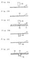
- a conductor wired layer (copper foil) 11 having a thickness of about 18 ⁇ m and a desired wired pattern in advance shown in Fig.2A, an opening 13 of about 100 ⁇ m is perforated by using a punch 12 (Fig.2B).
- a conductor layer 14 for forming bump made of, for example, metal copper is positioned on the copper foil 11 having the opening 13 (Fig.2C)
- a certain position of the conductor layer 14 corresponding to the opening 13 is pressed by using the punch 12 so that the conductor layer 14 is entered into the opening 13 and further a bump 15 is projected from the bottom surface of the conductor wired layer 11 as shown in Fig.2D.
- the opening formation and the bump formation may be conducted in a single operation by superposing the conductor layer for forming bump on the conductor wired layer before the opening formation and entering the conductor layer into the conductor wired layer by using the punch.
- the conductor wired layer 11 having a plurality of the bumps 15 is caulked such that the heights of the bumps from the bottom surface of the conductor wired layer 11 is made to be uniform and the top surface of the bump 15 is aligned with the top surface of the conductor wired layer 11 (Fig.2E).
- the conductor wired layer thus fabricated is integrated to an insulation substrate having through-holes (not shown) by means of adhesion to accomplish a print circuit board.
- an adhesive resin layer 17 is adhered on the bottom surface of the conductor wired layer 11 before the opening formation by using the punch (Fig.3A).
- a conductor wired layer having bumps including the adhesive resin layer 17 on the bump-projecting surface can be fabricated by way of opening 13 formation (Fig.3B), placement of the conductor layer 14 for forming bumps (Fig.3C), bump 15 formation (Fig. 3D), caulking (Fig.3E) and plated layer 16 formation (Fig.3F).
- a substrate 22 is made of a polyimide film having a copper-laminated layer 21 on its one surface.
- the copper-laminated layer 21 is patterned to form wired patterns 23 (Fig.4B).
- a plate-like conductive material 24 the same quality as an implant material for filling through-holes is positioned above the polyimide film 22.
- punches 25 having the sectional shapes the same as those of openings are positioned above the plate-like material and corresponding to the through-holes. Then, as shown in Fig.4C, these punches 25 moves downward.
- Each of the punches 25 penetrates the plate-like material 24 to hollow out the plate-like material as a pillar-like material having a sectional shape the same as that of the punch 25, and the pillar-like material is further moved downward by the punch 25.
- the punches 25 moving downward with the pillar-like material penetrate through-holes 26 and 27 through the wired patterns 23 and the polyimide film 22, respectively, and fill the through-holes 26 and 27 with the pillar-like material.
- the pillar-like material is projected from the bottom end of the though-holes having no wired patterns to form the bumps 28 made of the conductive material (Fig.4D).
- Copper-plated layers may be formed on the top and bottom surfaces of the substrate 22, and an adhesive agent layer 29 is laminated on the bottom surface (the surface having no wired pattern) of the substrate 22 including the projecting bumps 28.
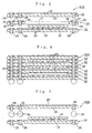
- a unit print circuit board is constituted by mounting an integrated circuit 31 on the wired patterns 23 of the substrate 22 via a plenty of small solder balls 30.
- a unit print circuit board 32A positioned in the upper part of Fig.5 has the same configuration as the unit print circuit board 32 of Fig.4 except for including no integrated circuit board, and a unit print circuit board 32 positioned in the lower part has the same configuration as the unit print circuit board 32 of Fig.4.
- a stacking frame 33 is sandwiched between both of the unit print circuit boards 32 and 32A.
- the overall contour of the stacking frame 33 is nearly the same as the shapes of the both unit print circuit boards 32 and 32A, and includes an inward aperture 34 larger than the integrated circuit 31.
- Through-holes 36 filled with conductive materials 35 having nearly the same shapes as those of the bumps 28 are formed at the positions of the stacking frame 33 corresponding to the bumps 28 of the unit print circuit board 32.
- the conductive material 35 projects downward similar to the bump 28 and penetrates through the adhesive agent layer 37 on the top surface.
- the formation of the through-holes 36 of the stacking frame filled with the conductive material 35 is preferably conducted in a single operation in which the aperture formation and the material filling are performed by using a punch, similarly to the bump formation in Fig.4.
- the three stacking frames 33 and the three unit print circuit board 32 are alternately positioned.
- a pressure is exerted thereto in the vertical direction under heating to melt and integrate the bump 28 of the unit print circuit board 32 and the conductive materials 35 of the stacking frame, thereby forming a longitudinally extending connecting material 38 to electrically connecting the respective unit print circuit boards 32.
- the fabrication of the CSP is accomplished.
- the productivity of the unit print circuit board and eventually the productivity of the CSP are increased different from those of the conventional method in which a though-hole is once formed and then the through-hole is filled by means of plating, because the bump filling into the through-holes 26 and 27 of the unit print circuit board 32 is conducted in the single operation using the punch.
- the use of the stacking frame is not essential, and a similar effect can be obtained by, for example as shown in Fig.7, placing the number of solder balls 39 in the positions corresponding to the conductive materials 35 in the stacking frame of Fig.5. Also in this case, the productivity of the unit print circuit board and eventually the productivity of the CSP are increased because the bump filling into the through-holes 26 and 27 of the unit print circuit board 32 is conducted in the single operation using the punch.
- a conductor wired layer having bump was fabricated with procedures shown in Fig.2.
- a plurality of openings having a diameter of about 100 ⁇ m were perforated through a copper foil (conductor wired layer) having a thickness of 18 ⁇ m by using a punch having a diameter of about 100 ⁇ m.
- a copper foil on the copper foil was superposed a copper foil (conductor layer for forming bump) having a thickness of about 130 ⁇ m.
- the copper foil (conductor layer for forming bump) was punched at the positions corresponding to the respective openings by using the above punch such that the copper foil is entered into the openings to be projected from the bottom edge of the openings and to form bumps, thereby obtaining a conductor wired layer with bumps. Lengths of the downward projection of the bumps were not uniform in the range of 100 to 130 ⁇ m.
- the conductor wired layer was caulked by using an ordinary caulking machine such that the lengths of the downward projection of the bumps were adjusted to be about 100 ⁇ m and the top surface of the bumps and the top surface of the conductor wired layer were aligned.
- CuSO 4 200g/liter
- the conductor wired layer with bumps thus fabricated was adhered to an insulation substrate having through-holes by using an adhesive agent available from Dow Corning Toray Silicone Co., Ltd., thereby obtaining a print circuit board.
- a polyimide film (trade name: Espanex, available from Nippon Steel Chemical Co., Ltd.) substrate with a width of 35 mm and a thickness of 50 ⁇ m having a copper foil with a thickness of 18 ⁇ m laminated on its one surface was used. After a desired wired pattern was formed on the surface of the polyimide film substrate by etching the copper foil, annealed oxygen free high conductivity copper having a plate-like shape was positioned above the substrate.
- a unit print circuit board was fabricated by laminating, on the whole surface thereof, an adhesive agent having a thickness of 50 ⁇ m available from Dow Corning Toray Silicone Co., Ltd.
- a stacking frame was fabricated as follows.
- Opening larger than the outer diameter of the above integrated circuit were perforated in the center of the Espanex having a width of 35 mm the same as that of the substrate.
- the adhesive agent was applied to a position of the stacking frame corresponding to the bumps, and similarly to the case of the substrate, through-holes having a diameter of 80 ⁇ m were perforated and immediately thereafter the through-holes were filled with annealed oxygen free high conductivity copper to project the oxygen free high conductivity copper from the bottom surface by 20 ⁇ m, thereby forming the stacking frame.
- the projected surface was plated with copper by 3 ⁇ m followed by tin plating by 0.5 ⁇ m, an adhesive agent was laminated on the whole surface having the projection by a thickness of 50 ⁇ m.
- the unit print circuit boards and the stacking frames were adhered with heating at 400°C under pressure by means of the alloy formation between the tin and the gold and the adhesive agent on the bump, thereby providing a CSP.
- the CSP fabrication neither through-hole formation by means of laser processing nor bump formation by means of electrolytic copper plating was necessary, and the bump could be formed in the single operation. Accordingly, the length of time for the operation was significantly reduced.
- a CSP was fabricated in accordance with Example 1 except that after the through-holes were perforated through the respective unit print circuit boards and the stacking frames by using the punch, the plate-like annealed oxygen free high conductivity copper was placed above the through-holes and the oxygen free high conductivity copper was hallowed out by using the punch to be filled in the through-holes.
- this Comparative Example neither through-hole formation by means of laser processing nor bump formation by means of electrolytic copper plating was necessary.
- Example 2 The mechanical strengths of the CSPs fabricated in Example 2 and Comparative Example 1 were measured, and there was no difference between them. It was apparent that no disadvantage arose even if the length of time for operation was significantly reduced by forming the bump by means of the single punching as Example 2.
Landscapes
- Engineering & Computer Science (AREA)
- Manufacturing & Machinery (AREA)
- Microelectronics & Electronic Packaging (AREA)
- Printing Elements For Providing Electric Connections Between Printed Circuits (AREA)
- Production Of Multi-Layered Print Wiring Board (AREA)
Applications Claiming Priority (5)
| Application Number | Priority Date | Filing Date | Title |
|---|---|---|---|
| JP2001126018 | 2001-04-24 | ||
| JP2001126018A JP2002324957A (ja) | 2001-04-24 | 2001-04-24 | プリント回路板及びその製造方法 |
| JP2001147781A JP2002343901A (ja) | 2001-05-17 | 2001-05-17 | Cspの製造方法 |
| JP2001147781 | 2001-05-17 | ||
| PCT/JP2002/004016 WO2002089540A1 (fr) | 2001-04-24 | 2002-04-23 | Carte de circuits imprimes |
Publications (1)
| Publication Number | Publication Date |
|---|---|
| EP1389897A1 true EP1389897A1 (fr) | 2004-02-18 |
Family
ID=26614091
Family Applications (1)
| Application Number | Title | Priority Date | Filing Date |
|---|---|---|---|
| EP02718637A Withdrawn EP1389897A1 (fr) | 2001-04-24 | 2002-04-23 | Carte de circuits imprimes |
Country Status (4)
| Country | Link |
|---|---|
| US (1) | US20040099441A1 (fr) |
| EP (1) | EP1389897A1 (fr) |
| TW (1) | TW573452B (fr) |
| WO (1) | WO2002089540A1 (fr) |
Cited By (1)
| Publication number | Priority date | Publication date | Assignee | Title |
|---|---|---|---|---|
| CN102017133B (zh) * | 2008-05-09 | 2012-10-10 | 国立大学法人九州工业大学 | 芯片尺寸两面连接封装件及其制造方法 |
Families Citing this family (9)
| Publication number | Priority date | Publication date | Assignee | Title |
|---|---|---|---|---|
| US6943446B2 (en) * | 2002-11-08 | 2005-09-13 | Lsi Logic Corporation | Via construction for structural support |
| US7129417B2 (en) * | 2004-04-29 | 2006-10-31 | International Business Machines Corporation | Method and structures for implementing customizable dielectric printed circuit card traces |
| JP2007287906A (ja) * | 2006-04-17 | 2007-11-01 | Elpida Memory Inc | 電極と電極の製造方法、及びこの電極を備えた半導体装置 |
| EP2416635A1 (fr) * | 2007-02-20 | 2012-02-08 | Dynamic Details, Inc. | Cartes de câblage imprimé multicouche avec des trous débouchants remplis de cuivre |
| US8039960B2 (en) * | 2007-09-21 | 2011-10-18 | Stats Chippac, Ltd. | Solder bump with inner core pillar in semiconductor package |
| US10037957B2 (en) | 2016-11-14 | 2018-07-31 | Amkor Technology, Inc. | Semiconductor device and method of manufacturing thereof |
| US11018024B2 (en) * | 2018-08-02 | 2021-05-25 | Nxp Usa, Inc. | Method of fabricating embedded traces |
| CN112261787B (zh) * | 2020-10-22 | 2022-03-18 | 江门崇达电路技术有限公司 | 一种大尺寸印制板的钻孔方法 |
| WO2023097455A1 (fr) * | 2021-11-30 | 2023-06-08 | 京东方科技集团股份有限公司 | Plaque arrière et son procédé de fabrication, module de rétroéclairage et dispositif d'affichage |
Family Cites Families (14)
| Publication number | Priority date | Publication date | Assignee | Title |
|---|---|---|---|---|
| US3750278A (en) * | 1970-07-17 | 1973-08-07 | Sylvania Electric Prod | Printed circuit board with through connection and method and machine for making the through connection |
| KR0179404B1 (ko) * | 1993-02-02 | 1999-05-15 | 모리시타 요이찌 | 세라믹기판과 그 제조방법 |
| JPH08222838A (ja) * | 1995-02-17 | 1996-08-30 | Mitsubishi Plastics Ind Ltd | 厚銅回路基板の製造方法 |
| JP2944449B2 (ja) * | 1995-02-24 | 1999-09-06 | 日本電気株式会社 | 半導体パッケージとその製造方法 |
| JP3197213B2 (ja) * | 1996-05-29 | 2001-08-13 | 松下電器産業株式会社 | プリント配線板およびその製造方法 |
| DE19681758B4 (de) * | 1996-06-14 | 2006-09-14 | Ibiden Co., Ltd. | Einseitiges Schaltkreissubstrat für mehrlagige Schaltkreisplatine, mehrlagige Schaltkreisplatine und Verfahren zur Herstellung selbiger |
| JP3889856B2 (ja) * | 1997-06-30 | 2007-03-07 | 松下電器産業株式会社 | 突起電極付きプリント配線基板の製造方法 |
| US6038133A (en) * | 1997-11-25 | 2000-03-14 | Matsushita Electric Industrial Co., Ltd. | Circuit component built-in module and method for producing the same |
| US6180881B1 (en) * | 1998-05-05 | 2001-01-30 | Harlan Ruben Isaak | Chip stack and method of making same |
| JP3250988B2 (ja) * | 1998-10-23 | 2002-01-28 | 株式会社鈴木 | フィルド・ビアを有する樹脂シートの製造方法 |
| JP2000332369A (ja) * | 1999-05-25 | 2000-11-30 | Mitsui Mining & Smelting Co Ltd | プリント回路板及びその製造方法 |
| JP4331830B2 (ja) * | 1999-08-24 | 2009-09-16 | 京セラ株式会社 | セラミック回路基板 |
| JP2001068617A (ja) * | 1999-08-27 | 2001-03-16 | Toshiba Corp | 半導体装置 |
| US6465084B1 (en) * | 2001-04-12 | 2002-10-15 | International Business Machines Corporation | Method and structure for producing Z-axis interconnection assembly of printed wiring board elements |
-
2002
- 2002-04-23 EP EP02718637A patent/EP1389897A1/fr not_active Withdrawn
- 2002-04-23 US US10/475,707 patent/US20040099441A1/en not_active Abandoned
- 2002-04-23 WO PCT/JP2002/004016 patent/WO2002089540A1/fr not_active Ceased
- 2002-04-24 TW TW91108463A patent/TW573452B/zh not_active IP Right Cessation
Non-Patent Citations (1)
| Title |
|---|
| See references of WO02089540A1 * |
Cited By (1)
| Publication number | Priority date | Publication date | Assignee | Title |
|---|---|---|---|---|
| CN102017133B (zh) * | 2008-05-09 | 2012-10-10 | 国立大学法人九州工业大学 | 芯片尺寸两面连接封装件及其制造方法 |
Also Published As
| Publication number | Publication date |
|---|---|
| TW573452B (en) | 2004-01-21 |
| US20040099441A1 (en) | 2004-05-27 |
| WO2002089540A1 (fr) | 2002-11-07 |
Similar Documents
| Publication | Publication Date | Title |
|---|---|---|
| US5976912A (en) | Fabrication process of semiconductor package and semiconductor package | |
| JP5188809B2 (ja) | 多層プリント配線板およびその製造方法 | |
| US5994773A (en) | Ball grid array semiconductor package | |
| KR101049390B1 (ko) | 다층 프린트 배선판 및 그 제조 방법 | |
| US7670962B2 (en) | Substrate having stiffener fabrication method | |
| US8069558B2 (en) | Method for manufacturing substrate having built-in components | |
| US7480151B2 (en) | Wiring board and method of manufacturing the same | |
| EP1107654A1 (fr) | Feuille pour carte de circuits imprimes, procede de formation de trou d'interconnexion, feuille de resine a trou d'interconnexion charge, carte de circuits imprimes et procede de fabrication associe | |
| KR20070084635A (ko) | 다층 프린트 배선 기판 및 그 제조 방법 | |
| EP1389897A1 (fr) | Carte de circuits imprimes | |
| US6708398B2 (en) | Substrate for use in package of semiconductor device, semiconductor package using the substrate, and methods for manufacturing the substrate and the semiconductor package | |
| KR100639737B1 (ko) | 회로 장치의 제조 방법 | |
| KR100671541B1 (ko) | 함침 인쇄회로기판 제조방법 | |
| JP2007035869A (ja) | Tab用テープキャリア | |
| EP1385363B1 (fr) | Carte de circuits imprimes et procede permettant sa realisation, et carte de circuits imprimes laminee | |
| JP4396839B2 (ja) | キャビティ構造プリント配線板とその製造方法及び実装構造 | |
| JP2002343901A (ja) | Cspの製造方法 | |
| JP3656590B2 (ja) | 半導体装置用テープキャリアの製造方法 | |
| JP3777687B2 (ja) | チップキャリア | |
| JP2004281752A (ja) | 片面回路基板の製造方法及び片面回路基板 | |
| JP2002324957A (ja) | プリント回路板及びその製造方法 | |
| JP2003303859A (ja) | 半導体装置用テープキャリアおよびその製造方法 |
Legal Events
| Date | Code | Title | Description |
|---|---|---|---|
| PUAI | Public reference made under article 153(3) epc to a published international application that has entered the european phase |
Free format text: ORIGINAL CODE: 0009012 |
|
| 17P | Request for examination filed |
Effective date: 20031108 |
|
| AK | Designated contracting states |
Kind code of ref document: A1 Designated state(s): AT BE CH CY DE DK ES FI FR GB GR IE IT LI LU MC NL PT SE TR |
|
| STAA | Information on the status of an ep patent application or granted ep patent |
Free format text: STATUS: THE APPLICATION HAS BEEN WITHDRAWN |
|
| 18W | Application withdrawn |
Effective date: 20070313 |