EP1396882A2 - Verfahren zum Herstellen eines integrierten elektronischen Bauteils und elektrische Vorrichtung mit solchem Bauteil - Google Patents
Verfahren zum Herstellen eines integrierten elektronischen Bauteils und elektrische Vorrichtung mit solchem Bauteil Download PDFInfo
- Publication number
- EP1396882A2 EP1396882A2 EP03292012A EP03292012A EP1396882A2 EP 1396882 A2 EP1396882 A2 EP 1396882A2 EP 03292012 A EP03292012 A EP 03292012A EP 03292012 A EP03292012 A EP 03292012A EP 1396882 A2 EP1396882 A2 EP 1396882A2
- Authority
- EP
- European Patent Office
- Prior art keywords
- volume
- substrate
- temporary
- chimney
- filling
- Prior art date
- Legal status (The legal status is an assumption and is not a legal conclusion. Google has not performed a legal analysis and makes no representation as to the accuracy of the status listed.)
- Withdrawn
Links
Images


Classifications
-
- H—ELECTRICITY
- H10—SEMICONDUCTOR DEVICES; ELECTRIC SOLID-STATE DEVICES NOT OTHERWISE PROVIDED FOR
- H10D—INORGANIC ELECTRIC SEMICONDUCTOR DEVICES
- H10D64/00—Electrodes of devices having potential barriers
- H10D64/60—Electrodes characterised by their materials
- H10D64/66—Electrodes having a conductor capacitively coupled to a semiconductor by an insulator, e.g. MIS electrodes
- H10D64/68—Electrodes having a conductor capacitively coupled to a semiconductor by an insulator, e.g. MIS electrodes characterised by the insulator, e.g. by the gate insulator
- H10D64/691—Electrodes having a conductor capacitively coupled to a semiconductor by an insulator, e.g. MIS electrodes characterised by the insulator, e.g. by the gate insulator comprising metallic compounds, e.g. metal oxides or metal silicates
-
- H—ELECTRICITY
- H10—SEMICONDUCTOR DEVICES; ELECTRIC SOLID-STATE DEVICES NOT OTHERWISE PROVIDED FOR
- H10D—INORGANIC ELECTRIC SEMICONDUCTOR DEVICES
- H10D64/00—Electrodes of devices having potential barriers
- H10D64/01—Manufacture or treatment
- H10D64/013—Manufacture or treatment of electrodes having a conductor capacitively coupled to a semiconductor by an insulator
- H10D64/01302—Manufacture or treatment of electrodes having a conductor capacitively coupled to a semiconductor by an insulator the insulator being formed after the semiconductor body, the semiconductor being silicon
- H10D64/01304—Manufacture or treatment of electrodes having a conductor capacitively coupled to a semiconductor by an insulator the insulator being formed after the semiconductor body, the semiconductor being silicon characterised by the conductor
- H10D64/01306—Manufacture or treatment of electrodes having a conductor capacitively coupled to a semiconductor by an insulator the insulator being formed after the semiconductor body, the semiconductor being silicon characterised by the conductor the conductor comprising a layer of silicon contacting the insulator, e.g. polysilicon
- H10D64/01308—Manufacture or treatment of electrodes having a conductor capacitively coupled to a semiconductor by an insulator the insulator being formed after the semiconductor body, the semiconductor being silicon characterised by the conductor the conductor comprising a layer of silicon contacting the insulator, e.g. polysilicon the conductor further comprising a non-elemental silicon additional conductive layer, e.g. a metal silicide layer formed by the reaction of silicon with an implanted metal
- H10D64/01312—Manufacture or treatment of electrodes having a conductor capacitively coupled to a semiconductor by an insulator the insulator being formed after the semiconductor body, the semiconductor being silicon characterised by the conductor the conductor comprising a layer of silicon contacting the insulator, e.g. polysilicon the conductor further comprising a non-elemental silicon additional conductive layer, e.g. a metal silicide layer formed by the reaction of silicon with an implanted metal the additional layer comprising a metal or metal silicide formed by deposition, i.e. without a silicidation reaction, e.g. sputter deposition
-
- H—ELECTRICITY
- H10—SEMICONDUCTOR DEVICES; ELECTRIC SOLID-STATE DEVICES NOT OTHERWISE PROVIDED FOR
- H10D—INORGANIC ELECTRIC SEMICONDUCTOR DEVICES
- H10D64/00—Electrodes of devices having potential barriers
- H10D64/01—Manufacture or treatment
- H10D64/013—Manufacture or treatment of electrodes having a conductor capacitively coupled to a semiconductor by an insulator
- H10D64/01302—Manufacture or treatment of electrodes having a conductor capacitively coupled to a semiconductor by an insulator the insulator being formed after the semiconductor body, the semiconductor being silicon
- H10D64/01304—Manufacture or treatment of electrodes having a conductor capacitively coupled to a semiconductor by an insulator the insulator being formed after the semiconductor body, the semiconductor being silicon characterised by the conductor
- H10D64/01316—Manufacture or treatment of electrodes having a conductor capacitively coupled to a semiconductor by an insulator the insulator being formed after the semiconductor body, the semiconductor being silicon characterised by the conductor the conductor comprising a layer of elemental metal contacting the insulator, e.g. Ta, W, Mo or Al
-
- H—ELECTRICITY
- H10—SEMICONDUCTOR DEVICES; ELECTRIC SOLID-STATE DEVICES NOT OTHERWISE PROVIDED FOR
- H10D—INORGANIC ELECTRIC SEMICONDUCTOR DEVICES
- H10D64/00—Electrodes of devices having potential barriers
- H10D64/01—Manufacture or treatment
- H10D64/013—Manufacture or treatment of electrodes having a conductor capacitively coupled to a semiconductor by an insulator
- H10D64/01302—Manufacture or treatment of electrodes having a conductor capacitively coupled to a semiconductor by an insulator the insulator being formed after the semiconductor body, the semiconductor being silicon
- H10D64/01304—Manufacture or treatment of electrodes having a conductor capacitively coupled to a semiconductor by an insulator the insulator being formed after the semiconductor body, the semiconductor being silicon characterised by the conductor
- H10D64/01318—Manufacture or treatment of electrodes having a conductor capacitively coupled to a semiconductor by an insulator the insulator being formed after the semiconductor body, the semiconductor being silicon characterised by the conductor the conductor comprising a layer of alloy material, compound material or organic material contacting the insulator, e.g. TiN
- H10D64/0132—Manufacture or treatment of electrodes having a conductor capacitively coupled to a semiconductor by an insulator the insulator being formed after the semiconductor body, the semiconductor being silicon characterised by the conductor the conductor comprising a layer of alloy material, compound material or organic material contacting the insulator, e.g. TiN the conductor being a metallic silicide
-
- H—ELECTRICITY
- H10—SEMICONDUCTOR DEVICES; ELECTRIC SOLID-STATE DEVICES NOT OTHERWISE PROVIDED FOR
- H10D—INORGANIC ELECTRIC SEMICONDUCTOR DEVICES
- H10D64/00—Electrodes of devices having potential barriers
- H10D64/01—Manufacture or treatment
- H10D64/013—Manufacture or treatment of electrodes having a conductor capacitively coupled to a semiconductor by an insulator
- H10D64/01302—Manufacture or treatment of electrodes having a conductor capacitively coupled to a semiconductor by an insulator the insulator being formed after the semiconductor body, the semiconductor being silicon
- H10D64/01304—Manufacture or treatment of electrodes having a conductor capacitively coupled to a semiconductor by an insulator the insulator being formed after the semiconductor body, the semiconductor being silicon characterised by the conductor
- H10D64/01324—Manufacture or treatment of electrodes having a conductor capacitively coupled to a semiconductor by an insulator the insulator being formed after the semiconductor body, the semiconductor being silicon characterised by the conductor characterised by the sectional shape, e.g. T or inverted-T
-
- H—ELECTRICITY
- H10—SEMICONDUCTOR DEVICES; ELECTRIC SOLID-STATE DEVICES NOT OTHERWISE PROVIDED FOR
- H10D—INORGANIC ELECTRIC SEMICONDUCTOR DEVICES
- H10D64/00—Electrodes of devices having potential barriers
- H10D64/01—Manufacture or treatment
- H10D64/013—Manufacture or treatment of electrodes having a conductor capacitively coupled to a semiconductor by an insulator
- H10D64/01302—Manufacture or treatment of electrodes having a conductor capacitively coupled to a semiconductor by an insulator the insulator being formed after the semiconductor body, the semiconductor being silicon
- H10D64/01332—Making the insulator
- H10D64/01336—Making the insulator on single crystalline silicon, e.g. chemical oxidation using a liquid
-
- H—ELECTRICITY
- H10—SEMICONDUCTOR DEVICES; ELECTRIC SOLID-STATE DEVICES NOT OTHERWISE PROVIDED FOR
- H10D—INORGANIC ELECTRIC SEMICONDUCTOR DEVICES
- H10D64/00—Electrodes of devices having potential barriers
- H10D64/01—Manufacture or treatment
- H10D64/017—Manufacture or treatment using dummy gates in processes wherein at least parts of the final gates are self-aligned to the dummy gates, i.e. replacement gate processes
-
- H—ELECTRICITY
- H10—SEMICONDUCTOR DEVICES; ELECTRIC SOLID-STATE DEVICES NOT OTHERWISE PROVIDED FOR
- H10D—INORGANIC ELECTRIC SEMICONDUCTOR DEVICES
- H10D64/00—Electrodes of devices having potential barriers
- H10D64/20—Electrodes characterised by their shapes, relative sizes or dispositions
- H10D64/27—Electrodes not carrying the current to be rectified, amplified, oscillated or switched, e.g. gates
- H10D64/311—Gate electrodes for field-effect devices
- H10D64/411—Gate electrodes for field-effect devices for FETs
- H10D64/511—Gate electrodes for field-effect devices for FETs for IGFETs
- H10D64/517—Gate electrodes for field-effect devices for FETs for IGFETs characterised by the conducting layers
- H10D64/518—Gate electrodes for field-effect devices for FETs for IGFETs characterised by the conducting layers characterised by their lengths or sectional shapes
-
- H—ELECTRICITY
- H10—SEMICONDUCTOR DEVICES; ELECTRIC SOLID-STATE DEVICES NOT OTHERWISE PROVIDED FOR
- H10D—INORGANIC ELECTRIC SEMICONDUCTOR DEVICES
- H10D64/00—Electrodes of devices having potential barriers
- H10D64/60—Electrodes characterised by their materials
- H10D64/66—Electrodes having a conductor capacitively coupled to a semiconductor by an insulator, e.g. MIS electrodes
- H10D64/665—Electrodes having a conductor capacitively coupled to a semiconductor by an insulator, e.g. MIS electrodes the conductor comprising a layer of elemental metal contacting the insulator, e.g. tungsten or molybdenum
-
- H—ELECTRICITY
- H10—SEMICONDUCTOR DEVICES; ELECTRIC SOLID-STATE DEVICES NOT OTHERWISE PROVIDED FOR
- H10D—INORGANIC ELECTRIC SEMICONDUCTOR DEVICES
- H10D84/00—Integrated devices formed in or on semiconductor substrates that comprise only semiconducting layers, e.g. on Si wafers or on GaAs-on-Si wafers
- H10D84/01—Manufacture or treatment
- H10D84/0123—Integrating together multiple components covered by H10D12/00 or H10D30/00, e.g. integrating multiple IGBTs
- H10D84/0126—Integrating together multiple components covered by H10D12/00 or H10D30/00, e.g. integrating multiple IGBTs the components including insulated gates, e.g. IGFETs
- H10D84/0165—Integrating together multiple components covered by H10D12/00 or H10D30/00, e.g. integrating multiple IGBTs the components including insulated gates, e.g. IGFETs the components including complementary IGFETs, e.g. CMOS devices
- H10D84/0172—Manufacturing their gate conductors
-
- H—ELECTRICITY
- H10—SEMICONDUCTOR DEVICES; ELECTRIC SOLID-STATE DEVICES NOT OTHERWISE PROVIDED FOR
- H10D—INORGANIC ELECTRIC SEMICONDUCTOR DEVICES
- H10D84/00—Integrated devices formed in or on semiconductor substrates that comprise only semiconducting layers, e.g. on Si wafers or on GaAs-on-Si wafers
- H10D84/01—Manufacture or treatment
- H10D84/02—Manufacture or treatment characterised by using material-based technologies
- H10D84/03—Manufacture or treatment characterised by using material-based technologies using Group IV technology, e.g. silicon technology or silicon-carbide [SiC] technology
- H10D84/038—Manufacture or treatment characterised by using material-based technologies using Group IV technology, e.g. silicon technology or silicon-carbide [SiC] technology using silicon technology, e.g. SiGe
-
- H—ELECTRICITY
- H10—SEMICONDUCTOR DEVICES; ELECTRIC SOLID-STATE DEVICES NOT OTHERWISE PROVIDED FOR
- H10P—GENERIC PROCESSES OR APPARATUS FOR THE MANUFACTURE OR TREATMENT OF DEVICES COVERED BY CLASS H10
- H10P90/00—Preparation of wafers not covered by a single main group of this subclass, e.g. wafer reinforcement
- H10P90/19—Preparing inhomogeneous wafers
- H10P90/1904—Preparing vertically inhomogeneous wafers
- H10P90/1906—Preparing SOI wafers
- H10P90/1914—Preparing SOI wafers using bonding
-
- H—ELECTRICITY
- H10—SEMICONDUCTOR DEVICES; ELECTRIC SOLID-STATE DEVICES NOT OTHERWISE PROVIDED FOR
- H10W—GENERIC PACKAGES, INTERCONNECTIONS, CONNECTORS OR OTHER CONSTRUCTIONAL DETAILS OF DEVICES COVERED BY CLASS H10
- H10W10/00—Isolation regions in semiconductor bodies between components of integrated devices
- H10W10/01—Manufacture or treatment
- H10W10/011—Manufacture or treatment of isolation regions comprising dielectric materials
- H10W10/014—Manufacture or treatment of isolation regions comprising dielectric materials using trench refilling with dielectric materials, e.g. shallow trench isolations
-
- H—ELECTRICITY
- H10—SEMICONDUCTOR DEVICES; ELECTRIC SOLID-STATE DEVICES NOT OTHERWISE PROVIDED FOR
- H10W—GENERIC PACKAGES, INTERCONNECTIONS, CONNECTORS OR OTHER CONSTRUCTIONAL DETAILS OF DEVICES COVERED BY CLASS H10
- H10W10/00—Isolation regions in semiconductor bodies between components of integrated devices
- H10W10/10—Isolation regions comprising dielectric materials
- H10W10/17—Isolation regions comprising dielectric materials formed using trench refilling with dielectric materials, e.g. shallow trench isolations
-
- H—ELECTRICITY
- H10—SEMICONDUCTOR DEVICES; ELECTRIC SOLID-STATE DEVICES NOT OTHERWISE PROVIDED FOR
- H10W—GENERIC PACKAGES, INTERCONNECTIONS, CONNECTORS OR OTHER CONSTRUCTIONAL DETAILS OF DEVICES COVERED BY CLASS H10
- H10W10/00—Isolation regions in semiconductor bodies between components of integrated devices
- H10W10/10—Isolation regions comprising dielectric materials
- H10W10/181—Semiconductor-on-insulator [SOI] isolation regions, e.g. buried oxide regions of SOI wafers
-
- H—ELECTRICITY
- H10—SEMICONDUCTOR DEVICES; ELECTRIC SOLID-STATE DEVICES NOT OTHERWISE PROVIDED FOR
- H10W—GENERIC PACKAGES, INTERCONNECTIONS, CONNECTORS OR OTHER CONSTRUCTIONAL DETAILS OF DEVICES COVERED BY CLASS H10
- H10W20/00—Interconnections in chips, wafers or substrates
- H10W20/01—Manufacture or treatment
- H10W20/031—Manufacture or treatment of conductive parts of the interconnections
- H10W20/056—Manufacture or treatment of conductive parts of the interconnections by filling conductive material into holes, grooves or trenches
-
- H—ELECTRICITY
- H10—SEMICONDUCTOR DEVICES; ELECTRIC SOLID-STATE DEVICES NOT OTHERWISE PROVIDED FOR
- H10W—GENERIC PACKAGES, INTERCONNECTIONS, CONNECTORS OR OTHER CONSTRUCTIONAL DETAILS OF DEVICES COVERED BY CLASS H10
- H10W20/00—Interconnections in chips, wafers or substrates
- H10W20/01—Manufacture or treatment
- H10W20/071—Manufacture or treatment of dielectric parts thereof
- H10W20/074—Manufacture or treatment of dielectric parts thereof of dielectric parts comprising thin functional dielectric layers, e.g. dielectric etch-stop, barrier, capping or liner layers
- H10W20/076—Manufacture or treatment of dielectric parts thereof of dielectric parts comprising thin functional dielectric layers, e.g. dielectric etch-stop, barrier, capping or liner layers in via holes or trenches
-
- H—ELECTRICITY
- H10—SEMICONDUCTOR DEVICES; ELECTRIC SOLID-STATE DEVICES NOT OTHERWISE PROVIDED FOR
- H10W—GENERIC PACKAGES, INTERCONNECTIONS, CONNECTORS OR OTHER CONSTRUCTIONAL DETAILS OF DEVICES COVERED BY CLASS H10
- H10W20/00—Interconnections in chips, wafers or substrates
- H10W20/01—Manufacture or treatment
- H10W20/071—Manufacture or treatment of dielectric parts thereof
- H10W20/074—Manufacture or treatment of dielectric parts thereof of dielectric parts comprising thin functional dielectric layers, e.g. dielectric etch-stop, barrier, capping or liner layers
- H10W20/077—Manufacture or treatment of dielectric parts thereof of dielectric parts comprising thin functional dielectric layers, e.g. dielectric etch-stop, barrier, capping or liner layers on sidewalls or on top surfaces of conductors
-
- H—ELECTRICITY
- H10—SEMICONDUCTOR DEVICES; ELECTRIC SOLID-STATE DEVICES NOT OTHERWISE PROVIDED FOR
- H10W—GENERIC PACKAGES, INTERCONNECTIONS, CONNECTORS OR OTHER CONSTRUCTIONAL DETAILS OF DEVICES COVERED BY CLASS H10
- H10W20/00—Interconnections in chips, wafers or substrates
- H10W20/01—Manufacture or treatment
- H10W20/071—Manufacture or treatment of dielectric parts thereof
- H10W20/081—Manufacture or treatment of dielectric parts thereof by forming openings in the dielectric parts
-
- H—ELECTRICITY
- H10—SEMICONDUCTOR DEVICES; ELECTRIC SOLID-STATE DEVICES NOT OTHERWISE PROVIDED FOR
- H10W—GENERIC PACKAGES, INTERCONNECTIONS, CONNECTORS OR OTHER CONSTRUCTIONAL DETAILS OF DEVICES COVERED BY CLASS H10
- H10W20/00—Interconnections in chips, wafers or substrates
- H10W20/01—Manufacture or treatment
- H10W20/071—Manufacture or treatment of dielectric parts thereof
- H10W20/081—Manufacture or treatment of dielectric parts thereof by forming openings in the dielectric parts
- H10W20/083—Manufacture or treatment of dielectric parts thereof by forming openings in the dielectric parts the openings being via holes penetrating underlying conductors
-
- H—ELECTRICITY
- H10—SEMICONDUCTOR DEVICES; ELECTRIC SOLID-STATE DEVICES NOT OTHERWISE PROVIDED FOR
- H10W—GENERIC PACKAGES, INTERCONNECTIONS, CONNECTORS OR OTHER CONSTRUCTIONAL DETAILS OF DEVICES COVERED BY CLASS H10
- H10W20/00—Interconnections in chips, wafers or substrates
- H10W20/01—Manufacture or treatment
- H10W20/071—Manufacture or treatment of dielectric parts thereof
- H10W20/093—Manufacture or treatment of dielectric parts thereof by modifying materials of the dielectric parts
- H10W20/097—Manufacture or treatment of dielectric parts thereof by modifying materials of the dielectric parts by thermally treating
Definitions
- the present invention relates to a method of manufacturing a integrated electronic component.
- MOS Metal-Oxide-Semiconductor
- a method of forming an outer shaped material determined on a substrate consists in depositing, in a first step, a substantially uniform layer of this material on the substrate, then, in a second step, to remove this material by etching outside part of the substrate defined by a mask.
- the engraving process must be chosen so that said material in its final form has conforming sides to the desired geometry, which can be, for example, flat sides and perpendicular to the surface of the substrate.
- the etching process used must be selective between the material deposited on the substrate and the substrate material itself, so to remove the material deposited outside the desired final shape, without remove material from the substrate.
- the surface of the substrate is changed during etching, preventing precise control of the height, relative to the surface of the substrate, of the deposited material remaining after the etching step.
- This selectivity represents a constraint in the choice component materials, which may be incompatible with some of the characteristics sought for said component.
- the Damascene process known to those skilled in the art, or its variant "Dual Damascene” is a second method of forming a pattern of shape determined on a substrate. This process consists of depositing on the substrate a layer of an external material in which a cavity is formed serving as a mold for the material to which a given shape must be conferred. The cavity is filled with the latter material, forming an excess at the above the cavity, in order to guarantee a complete filling thereof. The excess filling material is then removed by polishing.
- a disadvantage of the Damascene and “dual Damascene” processes comes from the final polishing. Indeed, the polishing speed depends on the removed material, i.e. external material or filling material, so that areas with a high density of patterns are eroded when polishing at a speed different from that of areas with lower pattern density. Loss of flatness of the polishing surface as a result, source of disparities within a series of manufactured components using this type of process. This loss of flatness after polishing may correspond to variations in thickness of the material layer external reaching 150 nanometers, incompatible with 0.10 technologies and 0.13 micrometer which require a control of this thickness at 10 nanometers, approximately. This flatness requirement will become even more severe for future integrated circuit manufacturing technologies.
- these variations in thickness can also cause insufficient removal, during polishing, of excess filler material.
- the filling material is conductor, residual parts of this excess can cause subsequently an electrical short circuit, during the use of the device electric which incorporates such a component.
- An object of the present invention therefore consists in producing patterns of materials determined on a substrate allowing precise control of geometric dimensions of said patterns.
- the volume into which the material of introduction is introduced. filling is separated from the access surface, so that the dimensions of the said volume initially fixed are definitively kept until the end of process for producing the electronic component.
- An advantage of the process of the invention is to eliminate the constraints relating to the choice of filling material, linked to the selectivity of techniques for removing the filling material from the material of the substrate and / or materials delimiting said volume. Indeed, the process of the invention does not include a step of removing the filling material from of said volume. In addition, according to the method, the filling material is formed after the temporary material has been removed, so that the removal step temporary material does not limit the choice of filling material.
- Another advantage of the process of the invention lies in the absence of chemical and solid particle pollution generated during steps a, b and c.
- the process is therefore compatible with a high level of purity of the materials the electronic component, in particular the filling material, necessary for obtaining electrical characteristics particularly demanding.
- Yet another advantage of the process of the invention is to allow heating of the substrate and of the materials present on the front substrate step c of the process. So the use of a filling material likely to be degraded by heat treatment is compatible with a heating at least some of the other component materials electronic, to give them specific properties.
- the chimney has a section parallel to the surface of the substrate significantly smaller than a projection of said volume on the surface of the substrate.
- the method of the invention then makes it possible to introduce the material of filling in said volume by a reduced opening, particularly compatible with the production of electronic components having a high level of integration.
- the chimney allows in addition to access to a buried part of the electronic component being embodiment, that is to say a part not adjacent to said access surface.
- the process of the invention is then particularly suitable for carrying out structures with several superimposed levels, contributing to a decrease in the cost of the electronic component, by reducing the size of the substrate.
- the method can comprise a formation, before step a, of a pattern on the surface of the substrate comprising said volume filled at least partially by the temporary material.
- a first method consists in forming said portion on another substrate, called temporary support, by successive deposits of suitable materials on this temporary support.
- Said portion initially carried by the support temporary is then transferred to the surface of the substrate intended to carry the electronic component, according to one of the known transfer methods of a person skilled in the art, such as, for example, the so-called molecular bonding process (also known as "wafer bonding").
- Temporary support is then removed, for example by polishing from a surface of the support temporary opposite said portion. This withdrawal may be possibly supplemented by plasma etching (or “dry etching”).
- At least part of said portion includes materials formed directly on the surface of the intended substrate to wear the electronic component.
- the access chimney to said volume is then formed in said portion by removal of at least one material external to said volume, between the access surface and said volume.
- the temporary material is then removed from said volume through the chimney using a withdrawal process known to those skilled in the art, such as, by example, an isotropic etching of the temporary material.
- a withdrawal process known to those skilled in the art, such as, by example, an isotropic etching of the temporary material.
- an engraving isotropic can be carried out by means of a plasma ("dry etching") penetrating by the chimney to the temporary material in said volume, or by introducing through the chimney a liquid solution incorporating chemical reagents determined (“chemical etching”).
- electrochemical etching can in particular be implemented works by applying an electrical voltage between the temporary material and an electrode immersed in the solution.
- Plasma components or chemical reagents in the solution used can be appropriately chosen to selectively eliminate or, at least, mainly the temporary material compared to the others materials of said portion, external to said volume.
- the material temporary can be chosen from the following materials: silicon, an alloy of silicon and germanium, silica and silicon nitride, for which selective removal processes with respect to materials external to said volume suitably selected are known to the skilled person.
- Said volume occupied by the temporary material can also be delimited, on at least part of its limit, by at least one material specific resistant to the evacuation of temporary material.
- This material specific then constitutes an isotropic etching barrier between the temporary material and a material of said portion external to said volume.
- a first material resistant to the evacuation of temporary material can, in particular, be initially placed in the form of a barrier layer between the temporary material and the substrate.
- a barrier layer between the temporary material and the substrate.
- Such a configuration allows to use in particular the same material for the substrate and for the material temporary such as, for example, silicon.
- said first barrier layer material can be removed between the evacuation steps of the temporary material and introduction of the filling material. Said volume then corresponds to a meeting of the space initially occupied by the material temporary and the space occupied by the barrier layer.
- the filling material can be simultaneously formed in said volume and in the chimney.
- complete filling of said volume by the filler may not be necessary.
- a deposit of the filling material on the internal walls of said volume may be sufficient, while leaving empty a central part of said volume.
- a material of coating is introduced into said volume before the filling material, at from second precursors brought by the chimney.
- a material coating can have different functions within the electronic component final or during its realization. Such functions are, for example, a improvement of the adhesion of the filling material to the materials of the walls of said volume, a function of promoter of growth of the material of filling during step c of the process, or else chemical isolation or between the substrate and the filling material.
- the method of the invention is particularly suitable for carrying out of field effect transistor grids.
- a material of electrically conductive filler and an insulating coating material can be used to form the grid and the insulation oxide of the transistor gate.
- the chimney is also at less partially filled with conductive filler, it can constitute an electrical connection connecting the gate of the final transistor.
- the invention also relates to an electronic component, produced according to a process as described above. It also relates to a device electric comprising such a component.
- Said component can be, in particular, a field effect transistor whose gate is developed using the method of the invention.
- MOS transistor field effect transistor
- the grid is made of metallic material.
- Such a metal grid gives the MOS transistor with dynamic characteristics superior to those of a equivalent MOS transistor whose gate is made of conductive polycrystalline silicon, and allows a particular reduction in the size of this type of transistors.
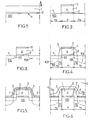
- a flat surface portion S of a substrate 100 is covered with a layer 2 of a first material.
- Layer 2 is itself covered with a layer of temporary material 1.
- the layers of temporary material 1 and of said first material 2 are substantially uniform over the surface portion S, of respective thicknesses 150 nanometers and 10 nanometers, for example , in direction D.
- Said first material of layer 2 is chosen to resist a process for removing the temporary material from layer 1.
- the temporary material is silicon
- said first material is silica SiO 2 .
- silica SiO 2 can also constitute the masking material 5.
- the masking material 5 and the temporary material 1 are then removed outside an area P1 of the substrate 100 (FIG. 2).
- This withdrawal is made according to one of the methods known to those skilled in the art, using by example a lithographed mask of resin covering the material 5 in the zone P1, then by exposing the substrate to at least one suitable etching plasma depending on the material 5 and then the material 1 being removed.
- This withdrawal defines the volume V, corresponding to the union of the space occupied by the temporary material 1 remaining in zone P1 after this etching and the space occupied by the part of the material 2 located between the temporary material 1 remaining and substrate 100.
- Temporary material 1 residual can be qualified of "false grid", since its role is to identify the location of the definitive transistor gate during part of the process of developing the transistor.
- the dimensions of this false grid parallel to the surface S are, for example, 15 to 130 nanometers in the plane of Figure 2 and 120 to 200 nanometers in the direction perpendicular to the plane of Figure 2.
- the material 2 is then removed from the surface S, in second zones P2 of the substrate which are separated from the first zone P1.
- the zones P2 can extend on either side of the zone P1, by being adjacent to the latter (FIG. 2).
- This removal of the material 2, in the case where it is silica, can be carried out by isotropic chemical etching, in particular of the flash type.
- Such an etching uses a solution containing hydrofluoric acid HF, optionally attenuated by ammonium fluoride NH 4 F.
- the second resistant material 3 is for example silicon nitride Si 3 N 4 , initially deposited in the form of a continuous layer covering the entire surface S, then etched isotropically in the direction D.
- the second resistant material 3 thus surrounds the false gate 1, parallel to the surface S, up to the height, in the direction D, of the upper surface of the masking material 5. It constitutes the spacer of the final transistor, disposed between the gate and the source of this transistor on the one hand, and between the gate and the drain of this transistor on the other hand.
- the surface S is then covered with a substantially uniform continuous layer 9 of a metal (FIG. 5).
- the metal used is chosen to form, when heated, a conductive alloy with silicon material on which it is deposited. Usually, cobalt is used and forms the CoSi 2 alloy. Other metals can alternatively be used, insofar as they form a similar conductive alloy with silicon.
- the metal-silicon alloy, or metal silicide is formed in the areas where the metal 9 is in direct contact with the silicon material of the substrate 100, that is to say in the areas P2 outside the areas P3.
- the spacer 3 and the masking material 5 prevent the formation of silicide from the silicon material of the false grid 1.
- the residual metal 9, apart from the parts of the metal 9 which formed the silicide, is eliminated by dissolution in an acidic chemical solution or by etching by means of a plasma accelerated against the surface S with a moderate electric voltage.
- the remaining zones 9bis of metal silicide form the electrical contact zones of the source and of the drain of the final transistor.
- a first external material 4 is then deposited, continuously and substantially uniformly in the zones P1 and P3, as well as in a fourth zone of the substrate surrounding the zone P3.
- the material 4 is deposited in the form of a layer covering the entire surface portion S, including the spacer 3 and the masking layer 5 above the volume V.
- Said fourth zone then corresponds to the zone complementary to zones P1 and P3 with respect to the whole of the surface portion S.
- the material 4 can be, in particular, silicon nitride Si 3 N 4 .
- the method for depositing the material 4 can be, for example, a method analogous to that used for the masking material 5.
- the thickness of the material 4 in the direction D is, for example, between 30 and 40 nanometers.
- the surface portion S is then covered with a layer of a second external material 6 up to, for example, a height of between 500 and 800 nanometers above the surface S of the substrate 100.
- This second external material can be chosen, in particular, to be deposited quickly. It can be, for example, silica SiO 2 obtained by chemical vapor deposition assisted by plasma (PECVD or "Plasma Enhanced Chemical Vapor Deposition").
- PECVD chemical vapor deposition assisted by plasma
- the upper surface of the material 6 is then polished so as to form a planar surface substantially parallel to the surface S of the substrate 100.
- the materials 3-6 constitute said portion of the process of the invention, referenced P in FIG. 6, with which the surface S of the substrate 100 is covered.
- the semiconductor properties of the implanted portions of the substrate 101-104 are definitively obtained only after specific heating at high temperature, for example at around 1000 ° C., called "activation annealing".
- This heating does not alter any of the materials carried by the substrate 100 at this level of execution of the process, these materials being polysilicon for the temporary material 1, silica SiO 2 for said first material 2 resistant to the evacuation of the material temporary and for the second external material 6, silicon nitride Si 3 N 4 for the second material 3 resistant to the evacuation of the temporary material, for the first external material 4 and for the masking material 5, and the metal silicide 9bis which has a refractory thermal behavior.
- a final metallic grid can be combined with the activation annealing at high temperature, in particular at a temperature higher than the melting temperature of the metal of the grid, the metal grid being formed after the activation annealing.
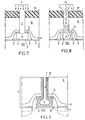
- a chimney C is then fitted between the upper surface of the second external material 6 and the volume V (FIG. 7).
- an etching mask M of resin is deposited on the material 6, comprising an opening intended to define the section of the chimney C parallel to the surface S.
- the substrate 100 carrying the mask M is then exposed to a directional etching plasma.
- a parallel flow of accelerated particles F1 is sent towards the substrate 100, which removes the successive materials appearing under the opening of the mask M. This removal is carried out according to a progression front perpendicular to the direction of the flow F1, and moving parallel to the direction of flow F1.
- the flow F1 is parallel to the direction D.
- Fluorinated molecules such as C 4 F 8 are introduced into the directional etching plasma to increase, by chemical effect, the etching speed of the second external material 6, in particular.
- the second external material 6 is thus removed in a column parallel to the direction D, then the first external material 4, and the masking material 5.
- the chimney C is thus formed.
- the substrate 100 still covered with the etching mask M is then exposed to an isotropic etching plasma of the material 1 of the false grid (FIG. 8).
- a plasma contains, for example, sulfur hexafluoride SF 6 or hydrogen chloride HCl molecules making it possible to selectively remove the silicon material 1 from the false grid without attacking the silica materials 2 and 6, nor the spacer 3 and the masking material 5 of silicon nitride.
- a flow of the particles of the isotropic etching plasma F2 enters the chimney C up to the volume V.
- the silicon material 1 of the false grid is thus gradually withdrawn along a peripheral front progressing in the volume V up to the walls thereof. defined by the spacer 3.
- the residual portion of the silica layer 2 prevents the withdrawal front from reaching the silicon material of the substrate 100, and is therefore called the stop layer.
- the mask M is removed.
- the residual portion of the silica layer 2 is then dissolved by chemical etching using the HF hydrofluoric acid solution already used for the etching of layer 2 in areas P2. For this, the solution is introduced through the chimney C and then removed after a sufficient reaction time to completely remove the remaining portion of layer 2.
- This second layer 2 removal step completes the recess of volume V after the evacuation of the temporary material 1.
- the section of the chimney C parallel to the surface S is slightly enlarged during this step, at the second external material 6, also made of silica. Otherwise, the lowering of the upper surface of the material 6 during this step is not not significant compared to the total thickness of the material 6.
- a coating material 8 (FIG. 9) is then introduced into the volume V from specific precursors supplied by the chimney C. These precursors include, for example, organometallic molecules gas reacting on contact with the exposed walls of volume V and the chimney C.
- precursors include, for example, organometallic molecules gas reacting on contact with the exposed walls of volume V and the chimney C.
- Several methods of forming material 8 can be used, such as chemical vapor deposition ("chemical vapor deposition "or CVD) or a deposition by superimposed atomic layers, known of the skilled person.
- the coating material 8 thus formed lines the volume V and the chimney C, as well as the upper surface of the material external 6.
- the material 8, intended to form an electrical insulation between the final grid and the substrate 100 perhaps, for example, hafnium oxide HfO 2 .
- This oxide indeed has a particularly high dielectric permittivity coefficient, favorable to a reduction in the thickness of the coating layer 8, while retaining effective electrical insulation.
- the thickness of hafnium oxide deposited is, for example, between 3 and 5 nanometers.
- the filling material 7 (FIG. 9) is formed in the volume V from suitable precursors introduced by the chimney C.
- the material of filling 7 is simultaneously formed in volume V and in the chimney C, on the exposed surface of the coating material 8.
- Several methods can also be used for the formation of material 8, the deposition of which chemical vapor phase, deposition by superimposed atomic layers, or yet another chemical deposition process known as "electroless".
- Such an “electroless” deposit, suitable for a filling material 7 metallic, proceeds by introducing a chemical solution into the chimney C.
- This solution comprises at least one precursor containing an atom of the metal in oxidized form, and a suitable reducing compound is added to the solution, which acts as a trigger for the release of the metal atom.
- chemical vapor deposition and layered deposition superimposed atomics are particularly suitable for a material 7 of tungsten, and the “electroless” process is particularly suitable for a material 7 of nickel or cobalt.
- an initial material 7 in the volume V can be formed as described above, then to transform in situ the initial material 7 to obtain a final material 7 having particular properties. This transformation can be carried out by heating the transistor after the formation of the initial material 7, or / and by bringing the initial material 7 into contact with at least one fluid chemical compound introduced into the volume V via the chimney C.
- the initial material 7 can be of the titanium nitride TiN x type , x being a stoichiometric number of between 0 and 1.
- x can then be adjusted by chemical reaction of the initial material 7 with a gas comprising nitrogen (N 2 ) and / or hydrogen (H 2 ), or alternatively ammonia (NH 3 ) brought while the transistor is brought to a sufficiently high temperature, in particular above 400 ° C.
- a gas comprising nitrogen (N 2 ) and / or hydrogen (H 2 ), or alternatively ammonia (NH 3 ) brought while the transistor is brought to a sufficiently high temperature, in particular above 400 ° C.
- the material 7 is chosen to be an electrical conductor, preferably metallic.
- the part of material 7 deposited in volume V corresponds to the gate of the MOS transistor, and the part of the material 7 deposited in the chimney constitutes an electrical connection connecting the gate of the transistor to the surface upper of the external material 6.
- a thickness of about 50 nanometers for the material 7 deposited provides sufficient electrical conduction for control the electrical voltage of the gate of the final transistor.
- metallic materials can be selected for the material 7, as a function of values of the electron output work listed for these materials. It may be particularly advantageous to establish symmetry of the trigger voltages of MOS transistors obtained by the process of the invention, of type n or p depending on the nature of the conduction of the grid, opposite to the type of doping of the silicon substrate 100 at the level of the source and drain (portions 101-104 of substrate 100). So a metal having an output work value located around 4 electron volts, such that aluminum, cadmium, hafnium, indium, magnesium, tantalum, zirconium, an alloy of titanium and tungsten, etc., is particularly suitable for an n-type MOS transistor, i.e. whose source and drain are doped p.
- a metal with an output working value located around 5.3 electron volts is particularly suitable, such as gold, platinum, palladium, ruthenium, rhodium or germanium.
- CMOS complementary MOS
- dual metal gate two gate metals
- Materials 7 and 8 present on the upper surface of the material external 6 are removed by polishing, so as to obtain the configuration shown in Figure 9.
- one of these two chimneys can partially lead to one end of the volume V, straddling the spacer 3.
- the use of a masking material 5 particularly dense and sufficiently resistant to the etching process directional then avoids an electrical short circuit between the grid and the source or drain, when filling the source and drain chimneys by the conductive material.
- an alignment error of the lithography mask used to define the position of the grate chimney C can move the axis of this parallel to the surface S of the substrate 100, so that the chimney C is located astride spacer 3, and partially leads to one of silicide zones 9bis.
- a short circuit electric analogous to that mentioned above can still appear.
- the first external material 4 is chosen so as to present a moderate withdrawal speed during directional etching of the chimney C. Due to the inclination of the outer surfaces of spacer 3 opposite the volume V, when the spacer 3 is produced in the manner described more top, the layer of external material 4 has a greater thickness in the portion P2 of the substrate around the spacer 3. The progression, according to the direction D, from the directional etching front of the chimney C is then slowed down in the portion P2 around the spacer 3, over a thickness of external material 4 greater than the thickness of material 4 above the volume V. Thus a chimney partially offset from volume V can nevertheless lead to volume V without reaching any of the zones 9bis silicide.
- This role of the layer of first external material 4, known under the name of "borderless”, is particularly combined advantageous with the method of the invention for obtaining transistors very small dimensions with good yield.
- the dimensions of a grid produced as described above are for example a width between 15 and 130 nanometers, and a length between 120 and 200 nanometers, corresponding to volume V.
- a projection of such a grid on the surface S is then a rectangle, which can for example be 25 nanometers by 180 nanometers.
- Figure 9 then corresponds to a section of such a grid perpendicular to its length.
- the chimney C can be cylindrical with a circular base, with a diameter of 15 nanometers for example, and can lead to the grid at proximity to one of its two short sides. Possibly, several fireplaces can be simultaneously used for the same grid having the previous dimensions, arranged for example at regular intervals on the length of this grid. Using multiple chimneys for the same grid notably facilitates the step of removing the temporary material 1, thus that the steps of introducing and depositing the coating materials 8 and filling 7 in volume V.
- the process of the invention is also particularly suitable for the realization, within the same integrated circuit, of MOS transistors having various individual characteristics, such as, for example, values respective different threshold voltage. It allows the realization of such transistors in a reduced number of steps. The price of manufacturing the circuit comprising these transistors of various characteristics is then lower than that of an equivalent circuit produced according to known methods.
- Separate threshold voltage values of a realized MOS transistor according to the invention can be obtained using two materials electrical conductors to make the transistor gate.
- the material of filling 7 then comprises first and second materials of filling electrical conductors successively introduced into the volume V, from the first respective precursors brought by the chimney C.
- first and second filling materials are deposited in volume V according to one of the methods described above in relation to the material of filling 7.
- they are deposited in chambers successive of the same integrated circuit manufacturing line tunnel.
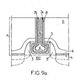
- FIG. 9a represents a MOS transistor thus obtained. Such transistor is identical to that shown in figure 9, apart from the constitution of the grid. This consists of two portions of materials filling 7a and 7b. Material 7a is arranged in the form of a layer covering the insulating coating layer 8 inside the volume V. The material 7b is placed on the layer of material 7a, in volume V. Des parts of material 7a and 7b deposited on the upper surface of material 6 are removed as described above for materials 7 and 8.
- the material 7a can be, for example, made of polysilicon, and the layer corresponding can have a thickness between 2 and 20 nanometers.
- the material 7b can be chosen from aluminum, cadmium, hafnium, indium, magnesium, tantalum, zirconium, an alloy of titanium and tungsten, gold, platinum, palladium, ruthenium, rhodium, germanium, or a compound comprising at least one of these metals.
- Material 7b can be placed inside the volume V in the form of a layer covering the layer of material 7a, for example around 40 nanometers thick, or so as to fill the volume V, or even until the chimney closes vs.
- Such a constitution of the grid makes it possible to adjust the threshold voltage of the MOS transistor, in particular by producing the material layer 7a with a low thickness and by choosing the material 7b appropriately.
- the threshold voltage of the transistor obtained is then intermediate between that of a transistor of the same configuration having a grid entirely in polysilicon, and that of a transistor of the same configuration having a grid made entirely of material 7b.
- the transistor can then be heated so as to cause a chemical reaction between materials 7a and 7b.
- a unique conductive material resulting from the chemical reaction can then constitute the transistor gate.
- a grid of tungsten silicide, of nickel or cobalt is obtained from a material 7a of silicon and a material 7b respectively of tungsten, nickel or cobalt.
- an integrated circuit in production includes several MOS transistors for which the step of introducing the filling material through their chimneys in order to constitute their respective grids, has not yet been performed.
- These MOS transistors still without grids have chimneys respective having different sections, considered in a parallel plane on the upper surface of the material 6. They can be, for example, distributed in a group of transistors with wide chimneys, that is to say with large sections, and a group of transistors with narrow chimneys, that is to say with small sections.
- the chimneys of the transistors of the two groups can be made in a single etching step, using a mask M formed on the material 6 which has an opening for each chimney, corresponding to the section of it.
- the respective volumes V of the transistors in two successive stages.
- the duration of this first stage is chosen so that the narrow C chimneys are essentially closed by material 7a, then that the wide C chimneys remain essentially open between the surface access and the respective volumes V of the transistors.
- the surface is exposed access of the circuit to the first precursors of the material 7b.
- Material 7b is then formed in the volumes V of the transistors whose respective chimneys C remained essentially open at the end of the first stage of the filling, i.e. wide chimney transistors.
- Portions of material 7b can also be deposited during this second step in an upper part of the narrow chimneys, if the chimneys are closed narrow by polysilicon during the first stage of filling is located below the level of the access surface. Such portions are then located in the narrow chimneys away from the grids corresponding, and have no influence on the electrical behavior of transistors thus obtained.
- Narrow chimney transistors therefore have grids consisting only of polysilicon, while the transistors at wide fireplaces have mixed grids made of polysilicon and of material 7b. Transistors of two types are thus produced in the circuit, differentiated by the dimensions of the sections of their chimneys respective, without requiring additional masking operations.
- the transistor can optionally be then heated, so as to cause a chemical reaction between the materials 7a and 7b in the respective volumes V of the chimney transistors wide.
- the method of the invention can also be used for carrying out tracks for the rapid transmission of electrical signals.
- Such leads are obtained by reducing the capacitive and inductive interactions between the metal parts that make up the tracks themselves and other materials close to these tracks.
- the disposal of materials with low dielectric permittivity near the tracks increases significantly the speed of transmission of electrical signals carried by tracks.
- Metal tracks can be made using the process Damascene, or the “dual Damascene” derivative process, known to man of the job.
- the metallic material of the tracks is preferably produced at high temperature, for example at minus 400 ° C, or brought to such a temperature after its preparation, in order to give it a crystallized structure.
- Gold materials with low permittivity dielectric such as polymers are degraded by heating to a temperature above about 250 ° C.
- the method of making fast signal transmission tracks electrical described below results from the use of the method of the invention, and allows the arrangement of a volume of polymer below tracks metallic at least partially crystallized.
- a volume V is formed in a substrate 100 by recess from a flat surface S of this substrate.
- the substrate 100 is for example made of silicon, and the volume V is hollowed out according to a method known to a person skilled in the art, comprising, for example, a covering of the surface S outside the volume V by a lithographed resin mask and a exposure of the surface S to a dry etching plasma.
- This etching plasma may contain molecules of sulfur hexafluoride SF 6 or of hydrogen chloride HCl, and is used so as to obtain a rapid directional etching of the silicon of the substrate 100.
- An alloy of silicon and germanium 1 is then deposited in the volume V so as to completely fill volume V ( Figure 11).
- a surface S is then polished to remove an excess of the alloy present on the surface S, and to obtain a final surface S rigorously plane.
- a portion P of circuit incorporating metal tracks is also produced on another substrate 200, for example also made of silicon (FIG. 12).
- This portion P comprises for example three layers of silica SiO 2 10 superimposed, within which metallic tracks 11 are produced, for example using the Damascene process.
- the tracks 11 can be made of copper or aluminum, in particular.
- the layers 10 and the tracks 11 carried by the substrate 200 are then heated, to a temperature above 400 ° C. for example, in order to create a crystallization of the metallic material of the tracks.
- various components not shown carried by the substrate 100 and capable of being degraded at high temperature are not subjected to this heating, and are thus preserved a risk of thermal degradation.
- Such components include, for example, zones of the substrate 100 implanted with doping elements which could diffuse thermally outside their initial implantation zone.
- the portion P is covered with a thin layer of silica SiO 2 10s, disposed on the upper face of the portion P opposite the substrate 200.
- the portion P is applied by the surface upper S 'of the layer 10s, opposite the substrate 200, on the surface S of the substrate 100 ( Figure 12).
- chemical bonds are then formed between the materials discovered at the level surfaces S and S ', brought into contact with each other. These links are in particular particularly numerous between the silicon of the substrate 100 and the silica of the layer 10s.
- Substrates 100 and 200 are then joined together (figure 13).
- the metal tracks 11 were initially arranged on the substrate 200 so as to be, at the end of the molecular bonding step, above the volume V formed in the substrate 100.
- the substrate 200 is then removed.
- This withdrawal includes for example a first phase of mechanical abrasion of substrate 200 over almost all the thickness of the substrate 200, this thickness being considered in the direction D.
- It then includes a second stage of dry etching, so as to remove the residual silicon thickness of the substrate 200, until the surface is discovered of the portion P opposite the substrate 100.
- the configuration shown in the Figure 14 is then obtained.
- a chimney C parallel to the direction D is formed through the portion P, from the upper surface of the portion P to volume V.
- a F1 flow of directional dry etching particles is sent through a resin mask M deposited on the portion P, with an opening defining the section of the chimney C (figure 15).
- the opening of the mask M is moreover arranged so that the chimney C crosses the portion P outside the metal tracks 11.
- Directional engraving is continued for one fixed duration, so that the chimney C formed reaches the volume V filled with silicon-germanium alloy.
- the etching mask M is removed.
- a selective etching solution of the silicon-germanium alloy is then introduced through the chimney C, up to volume V.
- an aqueous oxidizing solution composed of 40 milliliters of nitric acid HNO 3 at 70%, 20 milliliters of hydrogen peroxide H 2 O 2 and 5 milliliters of hydrofluoric acid HF at 5% causes the dissolution of the silicon-germanium alloy of volume V without altering the silicon material of the substrate 100, nor the other materials of portion P (figure 16).
- a polymer with low dielectric permittivity is then introduced by the chimney C and deposited in volume V, as a filling material 7 ( Figure 17).
- the polymer can be evaporated thermally from a solid source of this polymer placed in a crucible heated by Joule effect. Polymer molecules released under gaseous form then enter the chimney C and the volume V.
- the chimney C can also be filled with polymer during this deposit step.
- the volume V thus filled extends under the tracks 11, as well as on either side of the projection of the tracks 11 on the surface S in the direction D.
- the volume V is then the seat only very small electrostatic interactions with tracks 11 when these transmit electrical signals.
- the filling material 8 can be a dielectric material with low dielectric permittivity, in particular less than 1.40.
- the filling material 8 can be a compound of the silicon oxycarbide type SiO x C y , where x and y are the stoichiometric coefficients of oxygen and carbon respectively with respect to silicon.
- the filling material 8 can also be carbon having a structure analogous to that of diamond (“Diamond Like Carbon”), known to those skilled in the art under the acronym DLC.
Landscapes
- Electrodes Of Semiconductors (AREA)
- Insulated Gate Type Field-Effect Transistor (AREA)
Applications Claiming Priority (4)
| Application Number | Priority Date | Filing Date | Title |
|---|---|---|---|
| FR0211054 | 2002-09-06 | ||
| FR0211054A FR2844395A1 (fr) | 2002-09-06 | 2002-09-06 | Procede de realisation d'un composant electronique integre et dispositif electrique incorporant un composant integre ainsi obtenu |
| FR0302772 | 2003-03-06 | ||
| FR0302772A FR2844396B1 (fr) | 2002-09-06 | 2003-03-06 | Procede de realisation d'un composant electronique integre et dispositif electrique incorporant un composant integre ainsi obtenu |
Publications (2)
| Publication Number | Publication Date |
|---|---|
| EP1396882A2 true EP1396882A2 (de) | 2004-03-10 |
| EP1396882A3 EP1396882A3 (de) | 2007-09-05 |
Family
ID=31716900
Family Applications (1)
| Application Number | Title | Priority Date | Filing Date |
|---|---|---|---|
| EP03292012A Withdrawn EP1396882A3 (de) | 2002-09-06 | 2003-08-11 | Verfahren zum Herstellen eines integrierten elektronischen Bauteils und elektrische Vorrichtung mit solchem Bauteil |
Country Status (3)
| Country | Link |
|---|---|
| US (1) | US7041585B2 (de) |
| EP (1) | EP1396882A3 (de) |
| FR (1) | FR2844396B1 (de) |
Cited By (1)
| Publication number | Priority date | Publication date | Assignee | Title |
|---|---|---|---|---|
| EP1589572A1 (de) * | 2004-04-21 | 2005-10-26 | STMicroelectronics S.A. | Verfahren zur Herstellung einer integrierten Schaltung mit einem Isolationsgraben und entsprechende integrierte Schaltung |
Families Citing this family (4)
| Publication number | Priority date | Publication date | Assignee | Title |
|---|---|---|---|---|
| US20050145893A1 (en) * | 2003-12-29 | 2005-07-07 | Doczy Mark L. | Methods for fabricating metal gate structures |
| US8981496B2 (en) * | 2013-02-27 | 2015-03-17 | Taiwan Semiconductor Manufacturing Company, Ltd. | Metal gate and gate contact structure for FinFET |
| EP2802003B1 (de) * | 2013-05-07 | 2019-08-28 | IMEC vzw | Verfahren zur Bereitstellung einer Gate-Metallschicht einer Transistorvorrichtung |
| US10546847B2 (en) * | 2015-03-27 | 2020-01-28 | Fairchild Semiconductor Corporation | Substrate interposer on a leadframe |
Family Cites Families (19)
| Publication number | Priority date | Publication date | Assignee | Title |
|---|---|---|---|---|
| US38136A (en) * | 1863-04-07 | Improved burglar-alarm | ||
| US25638A (en) * | 1859-10-04 | Weighing-scale | ||
| JPS6353977A (ja) * | 1986-08-25 | 1988-03-08 | Toshiba Corp | 半導体装置の製造方法 |
| US5658816A (en) * | 1995-02-27 | 1997-08-19 | International Business Machines Corporation | Method of making DRAM cell with trench under device for 256 Mb DRAM and beyond |
| US6130482A (en) * | 1995-09-26 | 2000-10-10 | Fujitsu Limited | Semiconductor device and method for fabricating the same |
| US5976970A (en) * | 1996-03-29 | 1999-11-02 | International Business Machines Corporation | Method of making and laterally filling key hole structure for ultra fine pitch conductor lines |
| EP0890998A1 (de) | 1997-07-07 | 1999-01-13 | STMicroelectronics S.r.l. | Herstellungsverfahren und integrierter piezoresistiver Drucksensor mit einem Diaphragma aus polykristallinem Halbleitermaterial |
| US5943581A (en) * | 1997-11-05 | 1999-08-24 | Vanguard International Semiconductor Corporation | Method of fabricating a buried reservoir capacitor structure for high-density dynamic random access memory (DRAM) circuits |
| US6127712A (en) * | 1998-05-22 | 2000-10-03 | Texas Instruments--Acer Incorporated | Mosfet with buried contact and air-gap gate structure |
| JP3175700B2 (ja) * | 1998-08-24 | 2001-06-11 | 日本電気株式会社 | メタルゲート電界効果トランジスタの製造方法 |
| JP4237332B2 (ja) * | 1999-04-30 | 2009-03-11 | 株式会社東芝 | 半導体装置の製造方法 |
| TW495980B (en) * | 1999-06-11 | 2002-07-21 | Koninkl Philips Electronics Nv | A method of manufacturing a semiconductor device |
| US6319807B1 (en) * | 2000-02-07 | 2001-11-20 | United Microelectronics Corp. | Method for forming a semiconductor device by using reverse-offset spacer process |
| KR100367735B1 (ko) * | 2000-02-08 | 2003-01-10 | 주식회사 하이닉스반도체 | 집적 회로의 배선 구조 및 그 제조 방법 |
| US6303447B1 (en) * | 2000-02-11 | 2001-10-16 | Chartered Semiconductor Manufacturing Ltd. | Method for forming an extended metal gate using a damascene process |
| WO2001080286A2 (en) * | 2000-04-17 | 2001-10-25 | The Penn State Research Foundation | Deposited thin films and their use in separation and sarcrificial layer applications |
| US6335254B1 (en) * | 2000-08-09 | 2002-01-01 | Micron Technology, Inc. | Methods of forming transistors |
| JP2003243531A (ja) * | 2002-02-13 | 2003-08-29 | Mitsubishi Electric Corp | 半導体装置およびその製造方法 |
| US6645818B1 (en) * | 2002-11-13 | 2003-11-11 | Chartered Semiconductor Manufacturing Ltd. | Method to fabricate dual-metal gate for N- and P-FETs |
-
2003
- 2003-03-06 FR FR0302772A patent/FR2844396B1/fr not_active Expired - Fee Related
- 2003-08-07 US US10/638,228 patent/US7041585B2/en not_active Expired - Lifetime
- 2003-08-11 EP EP03292012A patent/EP1396882A3/de not_active Withdrawn
Cited By (1)
| Publication number | Priority date | Publication date | Assignee | Title |
|---|---|---|---|---|
| EP1589572A1 (de) * | 2004-04-21 | 2005-10-26 | STMicroelectronics S.A. | Verfahren zur Herstellung einer integrierten Schaltung mit einem Isolationsgraben und entsprechende integrierte Schaltung |
Also Published As
| Publication number | Publication date |
|---|---|
| US7041585B2 (en) | 2006-05-09 |
| FR2844396B1 (fr) | 2006-02-03 |
| FR2844396A1 (fr) | 2004-03-12 |
| US20040126977A1 (en) | 2004-07-01 |
| EP1396882A3 (de) | 2007-09-05 |
Similar Documents
| Publication | Publication Date | Title |
|---|---|---|
| EP2254146B1 (de) | Halbleiterstruktur und Herstellungsverfahren für eine Halbleiterstruktur | |
| EP1970950B1 (de) | Verfahren zur Herstellung einer Leiterstruktur mit luftgefüllten Zwischenräumen für integrierten Schaltkreis | |
| EP2096676A1 (de) | Verfahren zur Herstellung einer Halbleitervorrichtung mit vergrabenem Gitter und entsprechende integrierte Halbleiterschaltung | |
| EP0325808B1 (de) | Verfahren, um eine elektrische Verbindung auf einer Silizium-Halbleitervorrichtung herzustellen | |
| EP0351001A1 (de) | Verfahren zur Herstellung einer Halbleitervorrichtung mit mindestens einer kleine Kontaktlöcher enthaltenden Leiterbahn | |
| FR2524709A1 (fr) | Dispositif a semi-conducteur et procede pour sa fabrication | |
| FR2658951A1 (fr) | Procede de fabrication d'un circuit integre pour filiere analogique rapide utilisant des lignes d'interconnexions locales en siliciure. | |
| EP0463972A1 (de) | Verfahren zum Herstellen eines elektrischen Kontakts auf dem aktiven Element einer MIS-integrierten Schaltung | |
| EP1889296A1 (de) | Auf germanium basierender kanaltransistor mit einschliessung durch eine gate-elektrode und verfahren zur herstellung dieses transistors | |
| EP1346405B1 (de) | Verfahren zur herstellung einer zwischen elektroden eingefügten inselstruktur und deren anwendung auf transistoren | |
| EP1480266A2 (de) | Verfahren zur Herstellung integrierten Schaltungen mit gestapelten Bauteilen und entsprechende integrierte Schaltungen. | |
| EP4142459B1 (de) | Transistor mit josephson-effekt | |
| EP2045837B1 (de) | Selektive Bildung einer Verbindung, die ein Halbleitermaterial und ein Metallmaterial in einem Substrat enthält, mit Hilfe einer Germaniumoxydschicht | |
| EP2120258A1 (de) | Herstellungsverfahren eines Transistors mit Metallquelle und -abfluss | |
| EP1396882A2 (de) | Verfahren zum Herstellen eines integrierten elektronischen Bauteils und elektrische Vorrichtung mit solchem Bauteil | |
| FR2881575A1 (fr) | Transistor mos a grille totalement siliciuree | |
| EP0190243B1 (de) | Verfahren zur herstellung einer integrierten schaltung vom mis-typ | |
| EP4006996B1 (de) | Quantenvorrichtung und ihr herstellungsverfahren | |
| EP3136429B1 (de) | Herstellung von ohmschen kontakten für eine vorrichtung, die einen bereich aus iii-v-halbleitermaterial und einen bereich aus einem anderen halbleitermaterial enthält | |
| FR2844395A1 (fr) | Procede de realisation d'un composant electronique integre et dispositif electrique incorporant un composant integre ainsi obtenu | |
| EP4006997B1 (de) | Verfahren zur herstellung einer quantenvorrichtung | |
| FR2947384A1 (fr) | Procede de realisation d'un transistor a source et drain metalliques | |
| WO2005078785A1 (fr) | Procede de realisation d’un circuit electronique integre et circuit electronique integre ainsi obtenu | |
| FR2854276A1 (fr) | Dispositif semiconducteur comprenant des extensions realisees en un materiau a faible temperature de fusion. | |
| FR2717006A1 (fr) | Technologie de connexion sans contacts à fonctions multiples pour semi-conducteurs. |
Legal Events
| Date | Code | Title | Description |
|---|---|---|---|
| PUAI | Public reference made under article 153(3) epc to a published international application that has entered the european phase |
Free format text: ORIGINAL CODE: 0009012 |
|
| AK | Designated contracting states |
Kind code of ref document: A2 Designated state(s): AT BE BG CH CY CZ DE DK EE ES FI FR GB GR HU IE IT LI LU MC NL PT RO SE SI SK TR |
|
| AX | Request for extension of the european patent |
Extension state: AL LT LV MK |
|
| PUAL | Search report despatched |
Free format text: ORIGINAL CODE: 0009013 |
|
| AK | Designated contracting states |
Kind code of ref document: A3 Designated state(s): AT BE BG CH CY CZ DE DK EE ES FI FR GB GR HU IE IT LI LU MC NL PT RO SE SI SK TR |
|
| AX | Request for extension of the european patent |
Extension state: AL LT LV MK |
|
| 17P | Request for examination filed |
Effective date: 20080228 |
|
| AKX | Designation fees paid |
Designated state(s): DE GB IT |
|
| 17Q | First examination report despatched |
Effective date: 20090626 |
|
| STAA | Information on the status of an ep patent application or granted ep patent |
Free format text: STATUS: THE APPLICATION IS DEEMED TO BE WITHDRAWN |
|
| 18D | Application deemed to be withdrawn |
Effective date: 20091107 |