EP1429221A1 - Circuit intégré pour alimentation comportant un régulateur linéaire et un régulateur à découpage - Google Patents
Circuit intégré pour alimentation comportant un régulateur linéaire et un régulateur à découpage Download PDFInfo
- Publication number
- EP1429221A1 EP1429221A1 EP03028163A EP03028163A EP1429221A1 EP 1429221 A1 EP1429221 A1 EP 1429221A1 EP 03028163 A EP03028163 A EP 03028163A EP 03028163 A EP03028163 A EP 03028163A EP 1429221 A1 EP1429221 A1 EP 1429221A1
- Authority
- EP
- European Patent Office
- Prior art keywords
- regulator
- switching regulator
- series
- switching
- chip
- Prior art date
- Legal status (The legal status is an assumption and is not a legal conclusion. Google has not performed a legal analysis and makes no representation as to the accuracy of the status listed.)
- Ceased
Links
- 238000004891 communication Methods 0.000 claims description 23
- 238000001514 detection method Methods 0.000 claims description 6
- 230000001360 synchronised effect Effects 0.000 claims description 6
- 238000010586 diagram Methods 0.000 description 18
- 238000009499 grossing Methods 0.000 description 8
- 238000010276 construction Methods 0.000 description 7
- 230000004044 response Effects 0.000 description 6
- 239000003990 capacitor Substances 0.000 description 5
- 230000000694 effects Effects 0.000 description 5
- 230000001413 cellular effect Effects 0.000 description 2
- 235000019800 disodium phosphate Nutrition 0.000 description 1
- 238000012986 modification Methods 0.000 description 1
- 230000004048 modification Effects 0.000 description 1
- 230000009467 reduction Effects 0.000 description 1
- 239000000758 substrate Substances 0.000 description 1
Images


Classifications
-
- H—ELECTRICITY
- H04—ELECTRIC COMMUNICATION TECHNIQUE
- H04B—TRANSMISSION
- H04B1/00—Details of transmission systems, not covered by a single one of groups H04B3/00 - H04B13/00; Details of transmission systems not characterised by the medium used for transmission
- H04B1/38—Transceivers, i.e. devices in which transmitter and receiver form a structural unit and in which at least one part is used for functions of transmitting and receiving
- H04B1/40—Circuits
-
- G—PHYSICS
- G05—CONTROLLING; REGULATING
- G05F—SYSTEMS FOR REGULATING ELECTRIC OR MAGNETIC VARIABLES
- G05F1/00—Automatic systems in which deviations of an electric quantity from one or more predetermined values are detected at the output of the system and fed back to a device within the system to restore the detected quantity to its predetermined value or values, i.e. retroactive systems
- G05F1/10—Regulating voltage or current
- G05F1/46—Regulating voltage or current wherein the variable actually regulated by the final control device is DC
- G05F1/56—Regulating voltage or current wherein the variable actually regulated by the final control device is DC using semiconductor devices in series with the load as final control devices
-
- H—ELECTRICITY
- H02—GENERATION; CONVERSION OR DISTRIBUTION OF ELECTRIC POWER
- H02M—APPARATUS FOR CONVERSION BETWEEN AC AND AC, BETWEEN AC AND DC, OR BETWEEN DC AND DC, AND FOR USE WITH MAINS OR SIMILAR POWER SUPPLY SYSTEMS; CONVERSION OF DC OR AC INPUT POWER INTO SURGE OUTPUT POWER; CONTROL OR REGULATION THEREOF
- H02M3/00—Conversion of DC power input into DC power output
- H02M3/02—Conversion of DC power input into DC power output without intermediate conversion into AC
- H02M3/04—Conversion of DC power input into DC power output without intermediate conversion into AC by static converters
- H02M3/10—Conversion of DC power input into DC power output without intermediate conversion into AC by static converters using discharge tubes with control electrode or semiconductor devices with control electrode
- H02M3/145—Conversion of DC power input into DC power output without intermediate conversion into AC by static converters using discharge tubes with control electrode or semiconductor devices with control electrode using devices of a triode or transistor type requiring continuous application of a control signal
- H02M3/155—Conversion of DC power input into DC power output without intermediate conversion into AC by static converters using discharge tubes with control electrode or semiconductor devices with control electrode using devices of a triode or transistor type requiring continuous application of a control signal using semiconductor devices only
- H02M3/156—Conversion of DC power input into DC power output without intermediate conversion into AC by static converters using discharge tubes with control electrode or semiconductor devices with control electrode using devices of a triode or transistor type requiring continuous application of a control signal using semiconductor devices only with automatic control of output voltage or current, e.g. switching regulators
- H02M3/158—Conversion of DC power input into DC power output without intermediate conversion into AC by static converters using discharge tubes with control electrode or semiconductor devices with control electrode using devices of a triode or transistor type requiring continuous application of a control signal using semiconductor devices only with automatic control of output voltage or current, e.g. switching regulators including plural semiconductor devices as final control devices for a single load
- H02M3/1588—Conversion of DC power input into DC power output without intermediate conversion into AC by static converters using discharge tubes with control electrode or semiconductor devices with control electrode using devices of a triode or transistor type requiring continuous application of a control signal using semiconductor devices only with automatic control of output voltage or current, e.g. switching regulators including plural semiconductor devices as final control devices for a single load comprising at least one synchronous rectifier element
-
- H—ELECTRICITY
- H02—GENERATION; CONVERSION OR DISTRIBUTION OF ELECTRIC POWER
- H02M—APPARATUS FOR CONVERSION BETWEEN AC AND AC, BETWEEN AC AND DC, OR BETWEEN DC AND DC, AND FOR USE WITH MAINS OR SIMILAR POWER SUPPLY SYSTEMS; CONVERSION OF DC OR AC INPUT POWER INTO SURGE OUTPUT POWER; CONTROL OR REGULATION THEREOF
- H02M1/00—Details of apparatus for conversion
- H02M1/0045—Converters combining the concepts of switch-mode regulation and linear regulation, e.g. linear pre-regulator to switching converter, linear and switching converter in parallel, same converter or same transistor operating either in linear or switching mode
-
- Y—GENERAL TAGGING OF NEW TECHNOLOGICAL DEVELOPMENTS; GENERAL TAGGING OF CROSS-SECTIONAL TECHNOLOGIES SPANNING OVER SEVERAL SECTIONS OF THE IPC; TECHNICAL SUBJECTS COVERED BY FORMER USPC CROSS-REFERENCE ART COLLECTIONS [XRACs] AND DIGESTS
- Y02—TECHNOLOGIES OR APPLICATIONS FOR MITIGATION OR ADAPTATION AGAINST CLIMATE CHANGE
- Y02B—CLIMATE CHANGE MITIGATION TECHNOLOGIES RELATED TO BUILDINGS, e.g. HOUSING, HOUSE APPLIANCES OR RELATED END-USER APPLICATIONS
- Y02B70/00—Technologies for an efficient end-user side electric power management and consumption
- Y02B70/10—Technologies improving the efficiency by using switched-mode power supplies [SMPS], i.e. efficient power electronics conversion e.g. power factor correction or reduction of losses in power supplies or efficient standby modes
Definitions
- the present invention generally relates to a power supply IC having a plurality of power supply circuits, and particularly relates to a power supply IC having a series regulator for supplying power to high-frequency circuits and a switching regulator.
- the invention also relates to a communication apparatus in which such a power supply IC is employed.
- a switching regulator that functions as a noise source needs to be provided as a separate chip, separate from a power supply unit of the RF circuit that suffers trouble if affected by high-frequency noise. There should be provided some distance between these chips on the printed circuit board, or a filter should be provided between the chips, as a counter measure against the noise.
- the invention provides an integrated circuit for supplying power, including an IC chip having a rectangular shape and having a first edge and a second edge opposite the first edge, a switching regulator implemented on the IC chip and having a driver transistor whose ON time of switching is controlled to adjust an output voltage of the switching regulator, and a series regulator implemented on the IC chip, wherein the driver transistor of the switching regulator is positioned near the first edge, and the series regulator is positioned near the second edge.
- the series regulator includes a driver transistor whose conductivity of an ON state is controlled to adjust an output voltage of the series regulator.
- the series regulator supplies power to a high-frequency circuit.
- the switching regulator and the series regulator receive a positive power supply voltage through respective different pads.
- the switching regulator and the series regulator receive a negative power supply voltage through respective different pads.
- the integrated circuit as described above further includes additional circuitry situated between the driver transistor of the switching regulator and the series regulator.
- the driver transistor of the switching regulator and the series regulator are positioned near opposite corners of the IC chip.
- the driver transistor of the switching regulator and the series regulator are positioned near a diagonal line of the IC chip.
- the switching regulator functions as a DC-DC converter of a synchronous detection type.
- a communication apparatus includes an IC chip having a rectangular shape and having a first edge and a second edge opposite the first edge, a switching regulator implemented on the IC chip and having a driver transistor whose ON time of switching is controlled to adjust an output voltage of the switching regulator, a series regulator implemented on the IC chip, wherein the driver transistor of the switching regulator is positioned near the first edge, and the series regulator is positioned near the second edge, and a RF circuit unit including a transceiver for radio communication.
- the series regulator supplies power to the RF circuit.
- the switching regulator and the series regulator receive a positive power supply voltage through respective different pads.
- the switching regulator and the series regulator receive a negative power supply voltage through respective different pads.
- the communication apparatus as described above further includes additional circuitry situated between the driver transistor of the switching regulator and the series regulator.
- the driver transistor of the switching regulator and the series regulator are positioned near opposite corners of the IC chip.
- the driver transistor of the switching regulator and the series regulator are positioned near a diagonal line of the IC chip.
- the switching regulator functions as a DC-DC converter of a synchronous detection type.
- the driver transistor of the switching regulator is situated near an edge of the IC chip, and the series regulator is situated near the opposite edge of the IC chip. This provision reduces an effect of the noise generated by the switching regulator on the series regulator, thereby allowing the switching regulator and the series regulator to be implemented on a single IC. Further, an effect of the noise generated by the switching regulator is reduced on the high-frequency circuit that receives power from the series regulator. This improves the reliability of the power supply integrated circuit.
- the driver transistor of the switching regulator is situated near an edge of the IC chip, and the series regulator is situated near the opposite edge of the IC chip. This provision reduces an effect of the noise generated by the switching regulator on the series regulator, thereby reducing an effect on the signal processing of the high-frequency circuit that receives power from the series regulator, and also allowing the switching regulator and the series regulator to be implemented on a single IC. This helps to achieve the miniaturization of the communication apparatus.
- Fig. 1 is a block diagram showing an example of a communication apparatus in which a power supply IC according to a first embodiment of the invention is used.
- a cellular phone is shown as an example of a communication apparatus.
- a communication apparatus 1 includes a power supply circuit unit 2 having a plurality of power supply circuits, an audio circuit unit 3, a RF circuit unit 4 comprised of transceiver circuits and the like, a CPU logic circuit unit 5 for controlling the power supply circuit unit 2, the audio circuit unit 3, and the RF circuit unit 4, a display unit 6, an antenna 7, an operation unit 8 comprised of operation buttons, a speaker 9, a microphone 10, and a battery 11.
- the power supply circuit unit 2, the audio circuit unit 3, the RF circuit unit 4, and the CPU logic circuit unit 5 are molded on a single substrate, creating a single module 12.
- the power supply circuit unit 2 generates a predetermined constant voltage from the power supplied from the battery 11, and supplies power to the audio circuit unit 3, the RF circuit unit 4, and the CPU logic circuit unit 5.
- the CPU logic circuit unit 5 responds to instruction from the operation unit 8 by controlling the operations of the power supply circuit unit 2, the audio circuit unit 3, the RF circuit unit 4, and the display unit 6.
- the RF circuit unit 4 transmits and receives signals through the antenna 7.
- the audio circuit unit 3 receives signals from the microphone 10, and outputs signals to the speaker 9.
- Fig. 2 is a block diagram showing an example of the construction of the power supply circuit unit 2 shown in Fig. 1.
- Fig. 2 illustrates an example in which one switching regulator and three series regulators are provided.
- the power supply circuit unit 2 includes a switching regulator 21, series regulators SR1-SR3, a charge control circuit 22 for controlling the charging of the battery 11, and an SIM card interface circuit 23 for providing an interface between an SIM card 27 and the CPU logic circuit unit 5.
- the power supply circuit unit 2 further includes a power-on logic circuit 24, which controls the operations of the switching regulator 21, the series regulators SR1-SR3, the charge control circuit 22, and the SIM card interface circuit 23 in response to a positive power supply voltage Vbat supplied from the battery 11.
- the power supply circuit unit 2 is integrated as a single IC, except for few components which cannot be integrated. This IC serves as a power supply IC.
- the switching regulator 21, the series regulators SR1-SR3, and the SIM card interface circuit 23 receives power from the battery 11.
- the power-on logic circuit 24 monitors a positive power supply voltage Vbat of the battery 11.
- the charge control circuit 22 receives a DC voltage from an AC/DC adapter 28, and controls the charging of the battery 11 using the DC voltage.
- the power-on logic circuit 24 instructs the charge control circuit 22 to suppress the charging of the battery 11 if the positive power supply voltage Vbat of the battery 11 exceeds a predetermined level.
- the switching regulator 21 supplies power to the CPU logic circuit unit 5.
- the series regulators SR1 and SR2 supply power to the RF circuit unit 4.
- the series regulator SR3 supplies power to the audio circuit unit 3.
- the series regulators SR1 and SR2 are controlled by the CPU logic circuit unit 5 as to their enable status.
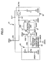
- Fig. 3 is a circuit diagram showing an example of the switching regulator 21.
- Fig. 3 shows an example in which the switching regulator 21 is provided as a DC-DC converter of the synchronous detection type.
- the switching regulator 21 in Fig. 3 includes a P-channel-type MOS transistor (hereinafter referred to as a PMOS transistor) 31 serving as a driver transistor for switching, an N-channel-type MOS transistor (hereinafter referred to as an NMOS transistor) 32 serving as a driver transistor for switching, and a smoothing circuit unit 33 which smoothes the output of the PMOS transistor 31 and the NMOS transistor 32 for outputting.
- a PMOS transistor P-channel-type MOS transistor
- NMOS transistor N-channel-type MOS transistor
- the switching regulator 21 further includes a reference voltage generating circuit unit 34 for generating and outputting a predetermined reference voltage Vr, a potential dividing circuit unit 35 for dividing a potential Vo output from the smoothing circuit unit 33 to generate and output a divided potential Vd, an error amplifier 36 for amplifying an error of the divided potential Vd with respect to the reference voltage Vr and for outputting the amplified error, and a control circuit unit 37 for the switching control of the PMOS transistor 31 and the NMOS transistor 32 in response to the output of the error amplifier 36.
- a reference voltage generating circuit unit 34 for generating and outputting a predetermined reference voltage Vr
- a potential dividing circuit unit 35 for dividing a potential Vo output from the smoothing circuit unit 33 to generate and output a divided potential Vd
- an error amplifier 36 for amplifying an error of the divided potential Vd with respect to the reference voltage Vr and for outputting the amplified error
- a control circuit unit 37 for the switching control of the PMOS transistor 31 and the NMOS transistor 32 in
- a pad VIN is coupled to the positive power supply voltage Vbat of the battery 11, and a pad GNDP is coupled to a negative power supply voltage GND of the battery 11.
- the PMOS transistor 31 and the NMOS transistor 32 are connected in series, with the gate of the PMOS transistor 31 and the gate of the NMOS transistor 32 being coupled to the control circuit unit 3, respectively.
- the junction of the PMOS transistor 31 and the NMOS transistor 32 is connected to a pad LX.
- a coil L and a capacitor C are connected in series, together forming the smoothing circuit unit 33.
- the junction of the coil L and capacitor C serves as an output terminal of the switching regulator 21, outputting a predetermined voltage Vo.
- the output voltage Vo is input into the potential dividing circuit unit 35 through a pad OUT for potential division by the potential dividing circuit unit 35.
- the divided potential Vd is supplied to one of the input ends of the error amplifier 36.
- the potential dividing circuit unit 35 includes a series connection of resistors R1 and R2. This series connection is situated between the pad OUT coupled to the output voltage Vo and a pad GNDA coupled to the negative power supply voltage GND.
- a junction of the resistors R1 and R2 is connected to one of the input ends of the error amplifier 36 for the provision of the divided potential Vd.
- the other input end of the error amplifier 36 receives the reference voltage Vr, and the output end of the error amplifier 36 is connected to the control circuit unit 37.
- the output voltage Vo is divided by the potential dividing circuit unit 35, and the error amplifier 36 amplifies a difference between the divided potential Vd and the reference voltage Vr.
- the control circuit unit 37 is equipped with an oscillator (not shown) for generating a saw-tooth pulse signal, for example, and a comparator (not shown).
- the comparator compares the output signal of the oscillator with the output signal of the error amplifier 36.
- the comparator controls the ON time of the PMOS transistor 31 and the NMOS transistor 32 in response to the comparison. In so doing, the control circuit unit 37 alternately switches on the PMOS transistor 31 and the NMOS transistor 32, without switching on both at the same time.
- the signal output from the junction of the PMOS transistor 31 and the NMOS transistor 32 is smoothed by the smoothing circuit unit 33 comprised of the coil L and the capacitor C for output as the output voltage Vo.
- Fig. 4 is a circuit diagram showing an example of the series regulators SR1-SR3.
- the series regulators SR1-SR3 all have the same circuit construction.
- the series regulator SRm in Fig. 4 includes a reference voltage generating circuit unit REm for generating and outputting a predetermined reference voltage Vrm, a potential dividing circuit unit DEm, an error amplifier AMPm, and a PMOS transistor Pm that serves as a driver transistor to provide a pad OUTm with an electric current responsive to a potential input into the gate from the error amplifier AMPm.
- the PMOS transistor Pm is situated between a pad Vddm coupled to the positive power supply voltage Vbat and a pad OUTm.
- a drain voltage of the PMOS transistor Pm is provided as an output voltage Vom.
- Resistors RAm and RBm, which together constitute the potential dividing circuit unit DEm, are connected in series between the pad OUTm and a pad GNDS coupled to the negative power supply voltage GND.
- the divided potential Vdm is output from the junction of the resistors RAm and RBm, and is input into the inverted input of the error amplifier AMPm.
- the non-inverted input of the error amplifier AMPm receives the reference voltage Vrm, and the output of the error amplifier AMPm is connected to the gate of the PMOS transistor Pm. Further, the error amplifier AMPm receives an enable signal SEm from the CPU logic circuit unit 5. When the enable signal SEm is asserted, the error amplifier AMPm stops operation, so that the PMOS transistor Pm becomes non-conductive, thereby stopping the supply of the output voltage Vom.
- the output voltage Vom is divided by the potential dividing circuit unit DEm.
- the error amplifier AMPm amplifies a difference between the divided potential Vdm and the reference voltage Vrm, and supplies its output to the gate of the PMOS transistor Pm. In this manner, the error amplifier AMPm controls the operation of the PMOS transistor Pm such as to keep the output voltage Vom at a desired voltage level.
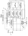
- Fig. 5 is a schematic diagram showing the power supply IC that corresponds to the power supply circuit unit 2 of Fig. 2.
- Fig. 5 illustrates an example of arrangement of the switching regulator 21 and the series regulators SR1-SR3 on an IC chip. A pad to which the enable signal SEm is supplied is omitted from illustration of Fig. 5.
- the PMOS transistor 31 (PMOSTr) and the NMOS transistor 32 (NMOSTr) of the switching regulator 21 are arranged near an edge 41 of a rectangular IC chip 40.
- the PMOS transistors P1-P3 of the respective series regulators SR1-SR3 are arranged near an edge 42 opposite the edge 41 of the IC chip 40.
- the switching regulator 21 and the series regulators SR1-SR3 are situated near a diagonal line of the IC chip 40 (i.e., situated near the opposite corners of the IC chip 40).
- the reference voltage generating circuit unit 34, the potential dividing circuit unit 35, the error amplifier 36, and the control circuit unit 37 of the switching regulator 21 are provided at the position of a controller 43 shown in Fig. 5, which is close to the PMOS transistor 31 and the NMOS transistor 32.
- the reference voltage generating circuit units RE1-RE3, the potential dividing circuit units DE1-DE3, and the error amplifiers AMP1-AMP3 of the respective series regulators SR1-SR3 are provided at the position of respective controllers 44-46 shown in Fig. 5, which are close to the respective PMOS transistors P1-P3.
- circuits of the power supply circuit unit 2 i.e., the charge control circuit 25, the SIM card interface circuit 26, and the power-on logic circuit 27, are arranged at a center portion 47 of the IC chip 40.
- the pads VDD, VIN, Vddl-Vdd3, and VddC are coupled to the positive power supply voltage Vbat of the battery 11.
- the pads GNDP, GNDA, GNDS, and GNDC are coupled to the negative power supply voltage GND of the battery 11.
- the coil L and the capacitor C of the smoothing circuit unit 33 are externally attached to the IC chip 40 through the pad LX.
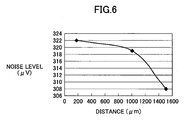
- Fig. 6 is a diagram showing the relationship between noise levels and the distance between the switching regulator oscillating at 800 kHz and the series regulators.
- a distance of 1.5 mm between the switching regulator and the series regulators provides a 5% noise reduction compared to when the distance between the switching regulator and the series regulators is 0.2 mm.
- the size of the power supply IC shown in Fig. 5 is 3 mm on a side.
- the driver transistor of the switching regulator 21 is arranged near the edge 41, and the driver transistors of the series regulators SR1-SR3 are arranged near the edge 42. With this provision, an effect of the noise generated by the switching regulator 21 on the series regulators SR1-SR3 is successfully reduced.
- a switching regulator functioning as a DC-DC converter of the synchronous detection type is used.
- a diode 51 may be used as a flywheel diode in place of the NMOS transistor 32.
- the switching regulator 21 of Fig. 3 has a construction as shown in Fig. 7.
- Fig. 7 the same elements as those of Fig. 3 are referred to by the same numerals and symbols.
- a switching regulator based on the use of a flywheel diode is well known in the art, and a description thereof will be omitted.
- a schematic diagram of the power supply IC is changed from that of Fig. 5 to that of Fig. 8.
- Fig. 8 the same elements as those of Fig. 5 are referred to by the same numerals and symbols, and a description thereof will be omitted. In what follows, differences will only be described.
- Fig. 8 differs from Fig. 5 in that the diode 51 serving as a flywheel diode is provided in place of the NMOS transistor 32. Other construction is the same, and a description thereof will be omitted.
- Fig. 3 and Fig. 7 are directed to a case in which a voltage-reduction-type switching regulator is employed. If a boosting-type switching regulator is used, the circuit construction will be changed to that of Fig. 9.
- Fig. 9 the same elements as those of Fig. 3 are referred to by the same numerals and symbols, and a description thereof will be omitted.
- Fig. 9 the same elements as those of Fig. 3 are referred to by the same numerals and symbols, and a description thereof will be omitted.
- the switching regulator 21 includes a NMOS transistor 61 serving as a switching transistor that switches in response to a control signal applied to the gate, a smoothing circuit unit 62 for smoothing the output signal of the NMOS transistor 61 for outputting of the smoothed signal, the reference voltage generating circuit unit 34, the potential dividing circuit unit 35, the error amplifier 36, and the control circuit unit 37 for the switching control of the NMOS transistor 61 in response to the output of the error amplifier 36.
- the output voltage Vo is divided by the potential dividing circuit unit 35, and the error amplifier 36 amplifies a difference between the divided potential Vd and the reference voltage Vr.
- the control circuit unit 37 is equipped with an oscillator (not shown) for generating a saw-tooth pulse signal, for example, and a comparator (not shown).
- the comparator compares the output signal of the oscillator with the output signal of the error amplifier 36.
- the comparator controls the ON time of the NMOS transistor 61 in response to the comparison.
- the signal output from the NMOS transistor 61 is smoothed by the smoothing circuit unit 62 comprised of a diode D2 serving as a rectifying diode, a coil L2, and a capacitor C2.
- the smoothed signal is output as the output voltage Vo.
- a schematic diagram of the power supply IC is changed from that of Fig. 5 to that of Fig. 10.
- Fig. 10 the same elements as those of Fig. 5 are referred to by the same numerals and symbols, and a description thereof will be omitted. In what follows, differences will only be described.
- Fig. 10 differs from Fig. 5 in that the PMOS transistor 31 is removed, and that the NMOS transistor 32 is replaced by the NMOS transistor 61. Other construction is the same, and a description thereof will be omitted.
- the above embodiment has been described with reference to a case in which one switching regulator and three series regulators are provided.
- the present invention is not limited to such a configuration, and is applicable to a case in which at least one switching regulator and at least one series regulator are provided.
Landscapes
- Engineering & Computer Science (AREA)
- Power Engineering (AREA)
- Physics & Mathematics (AREA)
- Electromagnetism (AREA)
- General Physics & Mathematics (AREA)
- Radar, Positioning & Navigation (AREA)
- Automation & Control Theory (AREA)
- Computer Networks & Wireless Communication (AREA)
- Signal Processing (AREA)
- Dc-Dc Converters (AREA)
- Continuous-Control Power Sources That Use Transistors (AREA)
- Semiconductor Integrated Circuits (AREA)
Applications Claiming Priority (2)
| Application Number | Priority Date | Filing Date | Title |
|---|---|---|---|
| JP2002362149 | 2002-12-13 | ||
| JP2002362149A JP4499985B2 (ja) | 2002-12-13 | 2002-12-13 | 電源用ic及びその電源用icを使用した通信装置 |
Publications (2)
| Publication Number | Publication Date |
|---|---|
| EP1429221A1 true EP1429221A1 (fr) | 2004-06-16 |
| EP1429221A8 EP1429221A8 (fr) | 2004-08-25 |
Family
ID=32322137
Family Applications (1)
| Application Number | Title | Priority Date | Filing Date |
|---|---|---|---|
| EP03028163A Ceased EP1429221A1 (fr) | 2002-12-13 | 2003-12-08 | Circuit intégré pour alimentation comportant un régulateur linéaire et un régulateur à découpage |
Country Status (4)
| Country | Link |
|---|---|
| US (2) | US7209770B2 (fr) |
| EP (1) | EP1429221A1 (fr) |
| JP (1) | JP4499985B2 (fr) |
| CN (1) | CN1510835B (fr) |
Cited By (2)
| Publication number | Priority date | Publication date | Assignee | Title |
|---|---|---|---|---|
| WO2006056640A1 (fr) * | 2004-11-23 | 2006-06-01 | Schneider Electric Industries Sas | Commutateur electronique a deux fils |
| CN113162819A (zh) * | 2021-02-22 | 2021-07-23 | 广东电网有限责任公司梅州供电局 | 10kV柱上开关成套设备联调方法、装置及存储介质 |
Families Citing this family (16)
| Publication number | Priority date | Publication date | Assignee | Title |
|---|---|---|---|---|
| JP4499985B2 (ja) * | 2002-12-13 | 2010-07-14 | 株式会社リコー | 電源用ic及びその電源用icを使用した通信装置 |
| JP4363938B2 (ja) * | 2003-09-26 | 2009-11-11 | シャープ株式会社 | 受信装置 |
| JP4673569B2 (ja) | 2004-03-31 | 2011-04-20 | 株式会社リコー | 半導体装置 |
| CN100505213C (zh) * | 2004-08-20 | 2009-06-24 | 罗姆股份有限公司 | 半导体器件及使用它的电源装置和电子设备 |
| JP4279766B2 (ja) * | 2004-10-19 | 2009-06-17 | 株式会社ルネサステクノロジ | レギュレータ内蔵送受信機を有する半導体装置およびモジュール |
| US7075343B2 (en) * | 2004-12-07 | 2006-07-11 | Analog Devices, Inc. | Self-timed switching regulator pre-driver |
| JP2007241777A (ja) * | 2006-03-10 | 2007-09-20 | Nec Corp | 温度補償レギュレータ回路 |
| JP2008211115A (ja) * | 2007-02-28 | 2008-09-11 | Ricoh Co Ltd | 半導体装置 |
| JP5364986B2 (ja) * | 2007-09-13 | 2013-12-11 | 株式会社リコー | 2次電池保護用半導体装置 |
| US7675357B2 (en) * | 2008-01-07 | 2010-03-09 | Azurewave Technologies, Inc. | Multi-system module having functional substrate |
| JP5363044B2 (ja) | 2008-07-22 | 2013-12-11 | ルネサスエレクトロニクス株式会社 | 半導体集積回路装置 |
| JP5779748B2 (ja) | 2010-11-02 | 2015-09-16 | リコー電子デバイス株式会社 | 半導体パッケージ及び電子部品実装体 |
| JP2016004347A (ja) * | 2014-06-16 | 2016-01-12 | ローム株式会社 | 半導体集積回路および電源装置 |
| JP6352733B2 (ja) * | 2014-08-28 | 2018-07-04 | ラピスセミコンダクタ株式会社 | 電源回路及びその制御方法 |
| JP7327998B2 (ja) * | 2019-05-17 | 2023-08-16 | ローム株式会社 | Dc/dcコンバータ |
| CN115706509B (zh) * | 2021-08-13 | 2023-10-27 | 中兴通讯股份有限公司 | 驱动装置和电子设备 |
Citations (3)
| Publication number | Priority date | Publication date | Assignee | Title |
|---|---|---|---|---|
| US5479089A (en) * | 1994-12-21 | 1995-12-26 | Hughes Aircraft Company | Power converter apparatus having instantaneous commutation switching system |
| US20020042902A1 (en) * | 1998-04-23 | 2002-04-11 | Matsushita Electric Industrial Co., Ltd. | Method for designing power supply circuit and semiconductor chip |
| US6438462B1 (en) * | 1996-03-26 | 2002-08-20 | Daimlerchrysler Ag | Semiconductor circuit for an electronic unit |
Family Cites Families (18)
| Publication number | Priority date | Publication date | Assignee | Title |
|---|---|---|---|---|
| US42902A (en) * | 1864-05-24 | Improvement in enveloped thread-clews | ||
| JPS61119071A (ja) * | 1984-11-15 | 1986-06-06 | Toshiba Corp | 半導体集積回路 |
| JPH03195055A (ja) * | 1989-12-25 | 1991-08-26 | Fujitsu Ltd | 半導体装置 |
| JPH046868A (ja) * | 1990-04-24 | 1992-01-10 | Fujitsu Ltd | 半導体集積回路 |
| JPH04123466A (ja) * | 1990-09-14 | 1992-04-23 | Hitachi Ltd | 半導体装置 |
| US5446367A (en) * | 1993-05-25 | 1995-08-29 | Micron Semiconductor, Inc. | Reducing current supplied to an integrated circuit |
| JPH11353040A (ja) * | 1998-04-10 | 1999-12-24 | Matsushita Electric Ind Co Ltd | 電源装置 |
| JP2001028430A (ja) * | 1999-07-13 | 2001-01-30 | Sanyo Electric Co Ltd | 半導体集積回路装置 |
| JP3394509B2 (ja) * | 1999-08-06 | 2003-04-07 | 株式会社リコー | 定電圧電源 |
| JP2001110184A (ja) | 1999-10-14 | 2001-04-20 | Hitachi Ltd | 半導体装置 |
| JP2001211640A (ja) * | 2000-01-20 | 2001-08-03 | Hitachi Ltd | 電子装置と半導体集積回路及び情報処理システム |
| JP2001313368A (ja) | 2000-04-28 | 2001-11-09 | Denso Corp | 集積回路 |
| JP4963144B2 (ja) * | 2000-06-22 | 2012-06-27 | ルネサスエレクトロニクス株式会社 | 半導体集積回路 |
| FR2811090B1 (fr) * | 2000-06-28 | 2002-10-11 | St Microelectronics Sa | Integration d'un regulateur de tension |
| JP2002110919A (ja) * | 2000-09-27 | 2002-04-12 | Toshiba Corp | 静電破壊保護回路 |
| JP4660921B2 (ja) * | 2000-12-14 | 2011-03-30 | 富士電機システムズ株式会社 | 電圧レギュレータ回路 |
| JP2003133972A (ja) * | 2001-10-29 | 2003-05-09 | Fujitsu Ltd | 無線送信機を有する電子装置 |
| JP4499985B2 (ja) * | 2002-12-13 | 2010-07-14 | 株式会社リコー | 電源用ic及びその電源用icを使用した通信装置 |
-
2002
- 2002-12-13 JP JP2002362149A patent/JP4499985B2/ja not_active Expired - Lifetime
-
2003
- 2003-12-04 US US10/726,626 patent/US7209770B2/en not_active Expired - Fee Related
- 2003-12-08 EP EP03028163A patent/EP1429221A1/fr not_active Ceased
- 2003-12-13 CN CN2003101097716A patent/CN1510835B/zh not_active Expired - Fee Related
-
2007
- 2007-03-13 US US11/717,131 patent/US7856253B2/en not_active Expired - Fee Related
Patent Citations (3)
| Publication number | Priority date | Publication date | Assignee | Title |
|---|---|---|---|---|
| US5479089A (en) * | 1994-12-21 | 1995-12-26 | Hughes Aircraft Company | Power converter apparatus having instantaneous commutation switching system |
| US6438462B1 (en) * | 1996-03-26 | 2002-08-20 | Daimlerchrysler Ag | Semiconductor circuit for an electronic unit |
| US20020042902A1 (en) * | 1998-04-23 | 2002-04-11 | Matsushita Electric Industrial Co., Ltd. | Method for designing power supply circuit and semiconductor chip |
Non-Patent Citations (2)
| Title |
|---|
| DOWLATABADI A B: "Challenges in CMOS mixed-signal designs for analog circuit designers", CIRCUITS AND SYSTEMS, 1997. PROCEEDINGS OF THE 40TH MIDWEST SYMPOSIUM ON SACRAMENTO, CA, USA 3-6 AUG. 1997, NEW YORK, NY, USA,IEEE, US, 3 August 1997 (1997-08-03), pages 47 - 50, XP010272484, ISBN: 0-7803-3694-1 * |
| SICARD E ET AL: "Cross-talk extraction from mask layout", DESIGN AUTOMATION, 1993, WITH THE EUROPEAN EVENT IN ASIC DESIGN. PROCEEDINGS. Y4TH EUROPEAN CONFERENCE ON PARIS, FRANCE 22-25 FEB. 1993, LOS ALAMITOS, CA, USA,IEEE COMPUTER SOCI, 22 February 1993 (1993-02-22), pages 414 - 418, XP010133217, ISBN: 0-8186-3410-3 * |
Cited By (3)
| Publication number | Priority date | Publication date | Assignee | Title |
|---|---|---|---|---|
| WO2006056640A1 (fr) * | 2004-11-23 | 2006-06-01 | Schneider Electric Industries Sas | Commutateur electronique a deux fils |
| CN113162819A (zh) * | 2021-02-22 | 2021-07-23 | 广东电网有限责任公司梅州供电局 | 10kV柱上开关成套设备联调方法、装置及存储介质 |
| CN113162819B (zh) * | 2021-02-22 | 2022-05-13 | 广东电网有限责任公司梅州供电局 | 10kV柱上开关成套设备联调方法、装置及存储介质 |
Also Published As
| Publication number | Publication date |
|---|---|
| EP1429221A8 (fr) | 2004-08-25 |
| US20070155444A1 (en) | 2007-07-05 |
| US7209770B2 (en) | 2007-04-24 |
| CN1510835A (zh) | 2004-07-07 |
| JP2004193475A (ja) | 2004-07-08 |
| US20040135626A1 (en) | 2004-07-15 |
| CN1510835B (zh) | 2010-10-13 |
| JP4499985B2 (ja) | 2010-07-14 |
| US7856253B2 (en) | 2010-12-21 |
Similar Documents
| Publication | Publication Date | Title |
|---|---|---|
| US7856253B2 (en) | Power supply IC having switching regulator and series regulator | |
| US7262588B2 (en) | Method and apparatus for power supply controlling capable of effectively controlling switching operations | |
| KR100767712B1 (ko) | 전자장치와 반도체집적회로 및 정보처리 시스템 | |
| CN101312304B (zh) | 送电装置以及电子设备 | |
| TWI468908B (zh) | 系統電源積體電路及架構、管理電路、電源供應配置以及手提裝置 | |
| US6774725B2 (en) | Power supply system for a high frequency power amplifier | |
| CN100474750C (zh) | 能够快速响应输入及输出电压变化的供电方法和电源设备 | |
| US7977974B2 (en) | Integrated circuit device and electronic instrument | |
| KR20080039874A (ko) | 강압형 스위칭 레귤레이터 및 그 제어 회로 및 그를 이용한전자 기기 | |
| JPH04211818A (ja) | 集積回路及び電子機器 | |
| JP2010526458A (ja) | Lnbのための電圧レギュレータ | |
| CN104868705B (zh) | 电子装置及其制造方法 | |
| US7602216B2 (en) | Integrated circuit device and electronic instrument | |
| CN1956289B (zh) | 半导体集成电路器件及使用该器件的非接触电子装置 | |
| US7378896B2 (en) | Single pin for multiple functional control purposes |
Legal Events
| Date | Code | Title | Description |
|---|---|---|---|
| PUAI | Public reference made under article 153(3) epc to a published international application that has entered the european phase |
Free format text: ORIGINAL CODE: 0009012 |
|
| 17P | Request for examination filed |
Effective date: 20031208 |
|
| AK | Designated contracting states |
Kind code of ref document: A1 Designated state(s): AT BE BG CH CY CZ DE DK EE ES FI FR GB GR HU IE IT LI LU MC NL PT RO SE SI SK TR |
|
| AX | Request for extension of the european patent |
Extension state: AL LT LV MK |
|
| RAP1 | Party data changed (applicant data changed or rights of an application transferred) |
Owner name: RICOH COMPANY, LTD. |
|
| AKX | Designation fees paid |
Designated state(s): DE ES FR GB IT NL |
|
| RBV | Designated contracting states (corrected) |
Designated state(s): DE ES FR GB IT NL |
|
| 17Q | First examination report despatched |
Effective date: 20071011 |
|
| RAP1 | Party data changed (applicant data changed or rights of an application transferred) |
Owner name: RICOH ELECTRONIC DEVICES CO., LTD. |
|
| STAA | Information on the status of an ep patent application or granted ep patent |
Free format text: STATUS: THE APPLICATION HAS BEEN REFUSED |
|
| 18R | Application refused |
Effective date: 20150926 |