EP1441446A2 - Stromzellenanordnung - Google Patents
Stromzellenanordnung Download PDFInfo
- Publication number
- EP1441446A2 EP1441446A2 EP04010234A EP04010234A EP1441446A2 EP 1441446 A2 EP1441446 A2 EP 1441446A2 EP 04010234 A EP04010234 A EP 04010234A EP 04010234 A EP04010234 A EP 04010234A EP 1441446 A2 EP1441446 A2 EP 1441446A2
- Authority
- EP
- European Patent Office
- Prior art keywords
- cell array
- cell
- cells
- array
- circuitry
- Prior art date
- Legal status (The legal status is an assumption and is not a legal conclusion. Google has not performed a legal analysis and makes no representation as to the accuracy of the status listed.)
- Granted
Links
- 238000003491 array Methods 0.000 claims abstract description 39
- 230000009466 transformation Effects 0.000 claims abstract description 13
- 238000009825 accumulation Methods 0.000 claims description 17
- 230000000694 effects Effects 0.000 abstract description 14
- 239000003990 capacitor Substances 0.000 description 14
- 230000035508 accumulation Effects 0.000 description 11
- 101100115778 Caenorhabditis elegans dac-1 gene Proteins 0.000 description 6
- 238000000034 method Methods 0.000 description 6
- 230000008901 benefit Effects 0.000 description 4
- 238000010586 diagram Methods 0.000 description 4
- 230000008569 process Effects 0.000 description 4
- 230000008859 change Effects 0.000 description 3
- 238000005513 bias potential Methods 0.000 description 2
- 238000010845 search algorithm Methods 0.000 description 2
- 230000003213 activating effect Effects 0.000 description 1
- 230000004913 activation Effects 0.000 description 1
- 238000006243 chemical reaction Methods 0.000 description 1
- 230000005669 field effect Effects 0.000 description 1
- 238000004519 manufacturing process Methods 0.000 description 1
- 239000011159 matrix material Substances 0.000 description 1
- 230000004044 response Effects 0.000 description 1
- 238000005070 sampling Methods 0.000 description 1
- 239000007787 solid Substances 0.000 description 1
- 238000000844 transformation Methods 0.000 description 1
- 230000001131 transforming effect Effects 0.000 description 1
Images







Classifications
-
- H—ELECTRICITY
- H03—ELECTRONIC CIRCUITRY
- H03M—CODING; DECODING; CODE CONVERSION IN GENERAL
- H03M1/00—Analogue/digital conversion; Digital/analogue conversion
- H03M1/06—Continuously compensating for, or preventing, undesired influence of physical parameters
- H03M1/0617—Continuously compensating for, or preventing, undesired influence of physical parameters characterised by the use of methods or means not specific to a particular type of detrimental influence
- H03M1/0634—Continuously compensating for, or preventing, undesired influence of physical parameters characterised by the use of methods or means not specific to a particular type of detrimental influence by averaging out the errors, e.g. using sliding scale
- H03M1/0643—Continuously compensating for, or preventing, undesired influence of physical parameters characterised by the use of methods or means not specific to a particular type of detrimental influence by averaging out the errors, e.g. using sliding scale in the spatial domain
- H03M1/0651—Continuously compensating for, or preventing, undesired influence of physical parameters characterised by the use of methods or means not specific to a particular type of detrimental influence by averaging out the errors, e.g. using sliding scale in the spatial domain by selecting the quantisation value generators in a non-sequential order, e.g. symmetrical
-
- H—ELECTRICITY
- H03—ELECTRONIC CIRCUITRY
- H03M—CODING; DECODING; CODE CONVERSION IN GENERAL
- H03M1/00—Analogue/digital conversion; Digital/analogue conversion
- H03M1/06—Continuously compensating for, or preventing, undesired influence of physical parameters
- H03M1/0617—Continuously compensating for, or preventing, undesired influence of physical parameters characterised by the use of methods or means not specific to a particular type of detrimental influence
- H03M1/0634—Continuously compensating for, or preventing, undesired influence of physical parameters characterised by the use of methods or means not specific to a particular type of detrimental influence by averaging out the errors, e.g. using sliding scale
- H03M1/0643—Continuously compensating for, or preventing, undesired influence of physical parameters characterised by the use of methods or means not specific to a particular type of detrimental influence by averaging out the errors, e.g. using sliding scale in the spatial domain
- H03M1/0648—Continuously compensating for, or preventing, undesired influence of physical parameters characterised by the use of methods or means not specific to a particular type of detrimental influence by averaging out the errors, e.g. using sliding scale in the spatial domain by arranging the quantisation value generators in a non-sequential pattern layout, e.g. symmetrical
-
- H—ELECTRICITY
- H03—ELECTRONIC CIRCUITRY
- H03M—CODING; DECODING; CODE CONVERSION IN GENERAL
- H03M1/00—Analogue/digital conversion; Digital/analogue conversion
- H03M1/66—Digital/analogue converters
- H03M1/74—Simultaneous conversion
- H03M1/742—Simultaneous conversion using current sources as quantisation value generators
- H03M1/747—Simultaneous conversion using current sources as quantisation value generators with equal currents which are switched by unary decoded digital signals
Definitions
- the present invention relates to cell array circuitry for use, for example, in digital-to-analog converters (DACs).
- DACs digital-to-analog converters
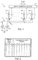
- FIG. 1 of the accompanying drawings shows parts of a conventional digital-to-analog converter (DAC) of the so-called "current-steering" type.
- the DAC 1 is designed to convert an m-bit digital input word (D1-Dm) into a corresponding analog output signal.
- thermometer-coded signals In order to avoid having to generate and supply different respective thermometer-coded signals to all the cells of the array, a two-stage decoding process is adopted to convert the binary input word D1-D6 into the respective thermometer-coded control signals T required by the differential switching circuits 4 in the different cells.
- the first stage of this two-stage decoding process is carried out by respective row and column decoders 12 and 14, and the second stage is carried out by a local decoder 16 provided for each cell.
- the numbers allotted to the cells CL ij in Figure 3 denote the sequence in which the cells are activated (or controlled) to change from selecting their respective second terminals to selecting their respective first terminals.
- the activation sequence follows the physical order of the cells in the array, starting from row 1 and activating the cells of that row sequentially in column order, followed by row 2, and so on for each successive row of the array.
- the selection means may, for example, be operable to select together each cell of the array whose said assigned ordinal position is less than a given value. For example, when the given value is i, the cells whose assigned ordinal positions are 1,2,...,i-1 are selected. It is convenient in this case if the said given value is determined by a selection signal (a digital input word) applied to the said selection means.
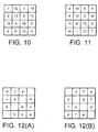
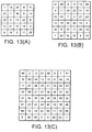
- the magic square may be pandiagonal and/or associative. This may give additional error-compensating effects depending on the mode of selection of the cells.
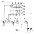
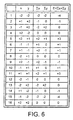
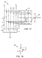
- each switch circuit has three terminals, the respective first terminals being connected in common to receive an input voltage V IN , the respective second terminals being connected in common to a negative reference voltage Vss, and the respective third terminals being connected in common to receive a predetermined reference potential V REF .
- Each switch circuit 46 is controllable, in dependence upon a selection signal S applied thereto, to connect its input node to one of its first, second and third terminals.
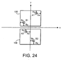
- a first cell array 100 made up of a plurality of individual cells arrayed in rows and columns, is placed in a first quadrant.
- Two representative cells A1 and B1 of the array 100 are shown in Figure 19, the cell A1 being spaced by distances Ax and Ay from the nearest edges in the x and y directions respectively, and the cell B1 being spaced from its nearest edges by distances Bx and By in the x and y directions respectively.
- a third cell array 104 is placed in a third quadrant.
- the arrangement of cells in the third cell array 104 is produced by reflecting the first cell array 100 about the x axis and then shifting the resulting reflection into the third quadrant.
- Representative cells A3 and B3, corresponding respectively to the representative cells A1 and B1 of the cell array 100, are shown in Figure 21.
- the cells are constituted by respective constant-current sources 2 and the four cells of a set are connected to a common connection line 110 that is connected to an input of the corresponding switch circuit.
Landscapes
- Engineering & Computer Science (AREA)
- Theoretical Computer Science (AREA)
- Analogue/Digital Conversion (AREA)
Applications Claiming Priority (3)
| Application Number | Priority Date | Filing Date | Title |
|---|---|---|---|
| GB9800367A GB2333190B (en) | 1998-01-08 | 1998-01-08 | Cell array circuitry |
| GB9800367 | 1998-01-08 | ||
| EP99300084A EP0929158B1 (de) | 1998-01-08 | 1999-01-06 | Stromzellenanordnung |
Related Parent Applications (1)
| Application Number | Title | Priority Date | Filing Date |
|---|---|---|---|
| EP99300084A Division EP0929158B1 (de) | 1998-01-08 | 1999-01-06 | Stromzellenanordnung |
Publications (3)
| Publication Number | Publication Date |
|---|---|
| EP1441446A2 true EP1441446A2 (de) | 2004-07-28 |
| EP1441446A3 EP1441446A3 (de) | 2004-08-11 |
| EP1441446B1 EP1441446B1 (de) | 2006-10-18 |
Family
ID=10825000
Family Applications (2)
| Application Number | Title | Priority Date | Filing Date |
|---|---|---|---|
| EP99300084A Expired - Lifetime EP0929158B1 (de) | 1998-01-08 | 1999-01-06 | Stromzellenanordnung |
| EP04010234A Expired - Lifetime EP1441446B1 (de) | 1998-01-08 | 1999-01-06 | Stromzellenanordnung |
Family Applications Before (1)
| Application Number | Title | Priority Date | Filing Date |
|---|---|---|---|
| EP99300084A Expired - Lifetime EP0929158B1 (de) | 1998-01-08 | 1999-01-06 | Stromzellenanordnung |
Country Status (5)
| Country | Link |
|---|---|
| US (1) | US6236346B1 (de) |
| EP (2) | EP0929158B1 (de) |
| JP (2) | JP4153115B2 (de) |
| DE (2) | DE69933712T2 (de) |
| GB (2) | GB2368209B (de) |
Families Citing this family (35)
| Publication number | Priority date | Publication date | Assignee | Title |
|---|---|---|---|---|
| JP4311511B2 (ja) * | 1999-10-25 | 2009-08-12 | 日本バーブラウン株式会社 | デジタル−アナログ変換の方法および装置 |
| GB2356301B (en) | 1999-11-10 | 2003-09-10 | Fujitsu Ltd | Data multiplexing in mixed-signal circuitry |
| GB2356302B (en) * | 1999-11-10 | 2003-11-05 | Fujitsu Ltd | Current switching circuitry |
| EP1492238B1 (de) | 1999-11-10 | 2006-05-24 | Fujitsu Limited | Schaltkreis zur digitalen Signalerregung |
| GB2356750B (en) | 1999-11-24 | 2002-12-04 | Fujitsu Ltd | Reducing jitter in mixed-signal circuitry |
| JP2001332973A (ja) * | 2000-03-16 | 2001-11-30 | Burr-Brown Japan Ltd | 共通の重み発生要素を用いたデジタル−アナログ変換の方法および装置 |
| DE60115003T2 (de) * | 2000-04-04 | 2006-08-10 | Koninklijke Philips Electronics N.V. | Ein digital-analog-wandler |
| US7280060B1 (en) | 2000-05-23 | 2007-10-09 | Marvell International Ltd. | Communication driver |
| US7095348B1 (en) | 2000-05-23 | 2006-08-22 | Marvell International Ltd. | Communication driver |
| US7113121B1 (en) | 2000-05-23 | 2006-09-26 | Marvell International Ltd. | Communication driver |
| US7194037B1 (en) | 2000-05-23 | 2007-03-20 | Marvell International Ltd. | Active replica transformer hybrid |
| US6775529B1 (en) | 2000-07-31 | 2004-08-10 | Marvell International Ltd. | Active resistive summer for a transformer hybrid |
| USRE41831E1 (en) | 2000-05-23 | 2010-10-19 | Marvell International Ltd. | Class B driver |
| US6462688B1 (en) | 2000-12-18 | 2002-10-08 | Marvell International, Ltd. | Direct drive programmable high speed power digital-to-analog converter |
| US7312739B1 (en) | 2000-05-23 | 2007-12-25 | Marvell International Ltd. | Communication driver |
| US7433665B1 (en) | 2000-07-31 | 2008-10-07 | Marvell International Ltd. | Apparatus and method for converting single-ended signals to a differential signal, and transceiver employing same |
| DE10032273C2 (de) * | 2000-07-03 | 2002-07-18 | Infineon Technologies Ag | Verfahren und Anordnung zur Kompensation von parasitären Stromverlusten |
| US7606547B1 (en) | 2000-07-31 | 2009-10-20 | Marvell International Ltd. | Active resistance summer for a transformer hybrid |
| JP2002100991A (ja) * | 2000-09-26 | 2002-04-05 | Nec Kyushu Ltd | D/aコンバータ |
| DE10052944C2 (de) * | 2000-10-25 | 2003-04-17 | Infineon Technologies Ag | Digital/Analog-Wandler |
| DE60119476T2 (de) | 2000-10-26 | 2006-11-23 | Fujitsu Ltd., Kawasaki | Segmentierte Schaltungsanordnung |
| EP1510009B1 (de) * | 2002-05-27 | 2006-10-18 | Nokia Corporation | Verfahren zum kalibrieren eines digital/analog-umsetzers und digital/analog-umsetzer |
| DE10331545A1 (de) * | 2003-07-11 | 2005-02-10 | Infineon Technologies Ag | Digital-Analog-Wandler und Verfahren zur Digital-Analog-Wandlung |
| US6911930B1 (en) * | 2003-12-15 | 2005-06-28 | Infineon Technologies Ag | Cell array with mismatch reduction |
| US7312662B1 (en) | 2005-08-09 | 2007-12-25 | Marvell International Ltd. | Cascode gain boosting system and method for a transmitter |
| JP5311021B2 (ja) * | 2006-11-07 | 2013-10-09 | 日本電気株式会社 | 電流出力型デジタル/アナログ変換回路、及び、映像表示装置 |
| JP5012728B2 (ja) | 2008-08-08 | 2012-08-29 | ソニー株式会社 | 表示パネルモジュール、半導体集積回路、画素アレイ部の駆動方法及び電子機器 |
| JP4618349B2 (ja) * | 2008-08-11 | 2011-01-26 | ソニー株式会社 | 固体撮像素子、撮像方法及び撮像装置 |
| US8446191B2 (en) * | 2009-12-07 | 2013-05-21 | Qualcomm Incorporated | Phase locked loop with digital compensation for analog integration |
| US8339165B2 (en) | 2009-12-07 | 2012-12-25 | Qualcomm Incorporated | Configurable digital-analog phase locked loop |
| US8766830B2 (en) | 2010-04-29 | 2014-07-01 | Agilent Technologies, Inc. | Digital waveform synthesizer for NMR phase control |
| CN102130687B (zh) * | 2010-12-29 | 2014-05-07 | 上海贝岭股份有限公司 | 一种数模转换器的电流源开关阵列的序列排布方法 |
| JP5832917B2 (ja) * | 2012-02-06 | 2015-12-16 | 株式会社メガチップス | 半導体集積回路および電流セルの配置方法 |
| CN105448963B (zh) * | 2015-12-04 | 2019-06-04 | 上海兆芯集成电路有限公司 | 晶体管以及电流源装置 |
| CN107863966B (zh) * | 2017-10-31 | 2021-02-05 | 电子科技大学 | 一种用于智能传感器的逐次逼近模数转换器电容优化方法 |
Family Cites Families (15)
| Publication number | Priority date | Publication date | Assignee | Title |
|---|---|---|---|---|
| US3995304A (en) * | 1972-01-10 | 1976-11-30 | Teledyne, Inc. | D/A bit switch |
| US4658240A (en) * | 1984-05-07 | 1987-04-14 | Brooktree Corporation | Apparatus for converting data between analog and digital values |
| JPS61240716A (ja) * | 1985-04-17 | 1986-10-27 | Mitsubishi Electric Corp | ディジタルアナログコンバ−タ |
| US4875046A (en) * | 1986-07-11 | 1989-10-17 | Brooktree Corporation | Centroiding algorithm for networks used in A/D and D/A converters |
| US4812818A (en) * | 1987-02-24 | 1989-03-14 | Brooktree Corporation | Digital-to-analog converter |
| US4859930A (en) * | 1988-02-16 | 1989-08-22 | Schouwenaars Hendrikus J | Current source arrangement |
| US5006854A (en) * | 1989-02-13 | 1991-04-09 | Silicon Systems, Inc. | Method and apparatus for converting A/D nonlinearities to random noise |
| JP2597712B2 (ja) * | 1989-05-22 | 1997-04-09 | 株式会社東芝 | ディジタル・アナログ変換器 |
| JP2641641B2 (ja) * | 1991-05-21 | 1997-08-20 | 三菱電機株式会社 | Da変換器 |
| DE4212621C2 (de) * | 1992-04-15 | 1994-06-30 | Texas Instruments Deutschland | Integrierter Digital/Analog-Umsetzer |
| US5568145A (en) | 1994-10-19 | 1996-10-22 | Analog Devices, Inc. | MOS current source layout technique to minimize deviation |
| US5977897A (en) * | 1996-12-31 | 1999-11-02 | Lucent Technologies Inc. | Resistor string with equal resistance resistors and converter incorporating the same |
| US5892471A (en) * | 1997-05-14 | 1999-04-06 | Texas Instruments Incorporated | Apparatus and method for current steering digital-to-analog converter units |
| US5949362A (en) * | 1997-08-22 | 1999-09-07 | Harris Corporation | Digital-to-analog converter including current cell matrix with enhanced linearity and associated methods |
| EP0903861B1 (de) * | 1997-09-19 | 2003-04-23 | Alcatel | Verfahren zur Auswahl einer Zellenfolge in einer zweidimensionalen Matrixstruktur eines Digital-Analog-Wandlers und nach diesem Verfahren arbeitender Wandler |
-
1998
- 1998-01-08 GB GB0202778A patent/GB2368209B/en not_active Expired - Fee Related
- 1998-01-08 GB GB9800367A patent/GB2333190B/en not_active Expired - Fee Related
- 1998-08-21 US US09/137,837 patent/US6236346B1/en not_active Expired - Lifetime
- 1998-12-25 JP JP36992498A patent/JP4153115B2/ja not_active Expired - Fee Related
-
1999
- 1999-01-06 DE DE69933712T patent/DE69933712T2/de not_active Expired - Lifetime
- 1999-01-06 DE DE69925768T patent/DE69925768T2/de not_active Expired - Lifetime
- 1999-01-06 EP EP99300084A patent/EP0929158B1/de not_active Expired - Lifetime
- 1999-01-06 EP EP04010234A patent/EP1441446B1/de not_active Expired - Lifetime
-
2008
- 2008-05-01 JP JP2008120026A patent/JP4408938B2/ja not_active Expired - Fee Related
Also Published As
| Publication number | Publication date |
|---|---|
| GB9800367D0 (en) | 1998-03-04 |
| JP4408938B2 (ja) | 2010-02-03 |
| GB2333190A (en) | 1999-07-14 |
| DE69925768T2 (de) | 2005-12-01 |
| DE69933712D1 (de) | 2006-11-30 |
| JP2008187748A (ja) | 2008-08-14 |
| JPH11243339A (ja) | 1999-09-07 |
| GB2368209A (en) | 2002-04-24 |
| JP4153115B2 (ja) | 2008-09-17 |
| EP1441446B1 (de) | 2006-10-18 |
| GB0202778D0 (en) | 2002-03-27 |
| GB2333190B (en) | 2002-03-27 |
| EP1441446A3 (de) | 2004-08-11 |
| EP0929158A3 (de) | 2002-11-06 |
| EP0929158A2 (de) | 1999-07-14 |
| DE69925768D1 (de) | 2005-07-21 |
| EP0929158B1 (de) | 2005-06-15 |
| US6236346B1 (en) | 2001-05-22 |
| GB2368209B (en) | 2002-06-12 |
| DE69933712T2 (de) | 2007-06-06 |
Similar Documents
| Publication | Publication Date | Title |
|---|---|---|
| EP0929158B1 (de) | Stromzellenanordnung | |
| Cong et al. | Switching sequence optimization for gradient error compensation in thermometer-decoded DAC arrays | |
| EP0898374B1 (de) | Digital-Analog-Wandler mit einer Stromquellenmatriz mit verbesserter Linearität und dazu gehörige Verfahren | |
| US6720898B1 (en) | Current source array for high speed, high resolution current steering DACs | |
| US5017919A (en) | Digital-to-analog converter with bit weight segmented arrays | |
| US5057838A (en) | D/a converter having centered switching sequence and centered arrangement of converter segment groups | |
| EP1191698B1 (de) | D/A-Wandler des Kapazitätsnetzwerkstyps mit Thermometerdekodierer und Kapazitätsnetzwerk | |
| Choi et al. | A 133.6 TOPS/W compute-in-memory SRAM macro with fully parallel one-step multi-bit computation | |
| Yenuchenko et al. | A switching sequence for unary digital-to-analog converters based on a knight’s tour | |
| US5568145A (en) | MOS current source layout technique to minimize deviation | |
| US20230370082A1 (en) | Shared column adcs for in-memory-computing macros | |
| Mohapatra et al. | Gradient error compensation in SC-MDACs | |
| Higashino et al. | Digital-to-analog converter layout technique and unit cell sorting algorithm for linearity improvement based on magic square | |
| Yenuchenko et al. | A 10-bit segmented M-string DAC | |
| US7633415B2 (en) | System and method for calibrating digital-to-analog convertors | |
| US20240037178A1 (en) | Compute-in-memory circuit with charge-domain passive summation and associated method | |
| CN109004934B (zh) | 一种阻容混合型数模转换器 | |
| Yenuchenko | Alternative structures of a segmented current-steering DAC | |
| US20240211536A1 (en) | Embedded matrix-vector multiplication exploiting passive gain via mosfet capacitor for machine learning application | |
| Yao | Segmented DAC Unit Cell Selection Algorithm and Layout/Routing Based on Classical Mathematics | |
| Mohapatra et al. | Mismatch resilient 3.5-bit MDAC with MCS-CFCS | |
| KR20240175728A (ko) | 인메모리 컴퓨팅 매크로용 공유 열 | |
| US7068194B1 (en) | High-density MOS-decoded unary DAC | |
| Zaki et al. | A Compact 12-bit Current-Steering D/A Converter for HDRC® Image Sensors | |
| JPH09130243A (ja) | アナログ−デジタル・コンバータ信号蓄積コンデンサ摂動 |
Legal Events
| Date | Code | Title | Description |
|---|---|---|---|
| PUAI | Public reference made under article 153(3) epc to a published international application that has entered the european phase |
Free format text: ORIGINAL CODE: 0009012 |
|
| PUAL | Search report despatched |
Free format text: ORIGINAL CODE: 0009013 |
|
| AC | Divisional application: reference to earlier application |
Ref document number: 0929158 Country of ref document: EP Kind code of ref document: P |
|
| AK | Designated contracting states |
Kind code of ref document: A2 Designated state(s): AT BE DE FI FR IE IT SE |
|
| AK | Designated contracting states |
Kind code of ref document: A3 Designated state(s): AT BE DE FI FR IE IT SE |
|
| 17P | Request for examination filed |
Effective date: 20050208 |
|
| AKX | Designation fees paid |
Designated state(s): DE FI FR IE IT SE |
|
| RBV | Designated contracting states (corrected) |
Designated state(s): DE FI FR IE IT SE |
|
| GRAC | Information related to communication of intention to grant a patent modified |
Free format text: ORIGINAL CODE: EPIDOSCIGR1 |
|
| GRAP | Despatch of communication of intention to grant a patent |
Free format text: ORIGINAL CODE: EPIDOSNIGR1 |
|
| GRAS | Grant fee paid |
Free format text: ORIGINAL CODE: EPIDOSNIGR3 |
|
| GRAA | (expected) grant |
Free format text: ORIGINAL CODE: 0009210 |
|
| AC | Divisional application: reference to earlier application |
Ref document number: 0929158 Country of ref document: EP Kind code of ref document: P |
|
| AK | Designated contracting states |
Kind code of ref document: B1 Designated state(s): DE FI FR IE IT SE |
|
| PG25 | Lapsed in a contracting state [announced via postgrant information from national office to epo] |
Ref country code: IT Free format text: LAPSE BECAUSE OF FAILURE TO SUBMIT A TRANSLATION OF THE DESCRIPTION OR TO PAY THE FEE WITHIN THE PRESCRIBED TIME-LIMIT;WARNING: LAPSES OF ITALIAN PATENTS WITH EFFECTIVE DATE BEFORE 2007 MAY HAVE OCCURRED AT ANY TIME BEFORE 2007. THE CORRECT EFFECTIVE DATE MAY BE DIFFERENT FROM THE ONE RECORDED. Effective date: 20061018 Ref country code: FI Free format text: LAPSE BECAUSE OF FAILURE TO SUBMIT A TRANSLATION OF THE DESCRIPTION OR TO PAY THE FEE WITHIN THE PRESCRIBED TIME-LIMIT Effective date: 20061018 |
|
| REG | Reference to a national code |
Ref country code: IE Ref legal event code: FG4D |
|
| REF | Corresponds to: |
Ref document number: 69933712 Country of ref document: DE Date of ref document: 20061130 Kind code of ref document: P |
|
| PG25 | Lapsed in a contracting state [announced via postgrant information from national office to epo] |
Ref country code: SE Free format text: LAPSE BECAUSE OF FAILURE TO SUBMIT A TRANSLATION OF THE DESCRIPTION OR TO PAY THE FEE WITHIN THE PRESCRIBED TIME-LIMIT Effective date: 20070118 |
|
| EN | Fr: translation not filed | ||
| PLBE | No opposition filed within time limit |
Free format text: ORIGINAL CODE: 0009261 |
|
| STAA | Information on the status of an ep patent application or granted ep patent |
Free format text: STATUS: NO OPPOSITION FILED WITHIN TIME LIMIT |
|
| 26N | No opposition filed |
Effective date: 20070719 |
|
| PG25 | Lapsed in a contracting state [announced via postgrant information from national office to epo] |
Ref country code: FR Free format text: LAPSE BECAUSE OF FAILURE TO SUBMIT A TRANSLATION OF THE DESCRIPTION OR TO PAY THE FEE WITHIN THE PRESCRIBED TIME-LIMIT Effective date: 20070601 |
|
| PG25 | Lapsed in a contracting state [announced via postgrant information from national office to epo] |
Ref country code: FR Free format text: LAPSE BECAUSE OF FAILURE TO SUBMIT A TRANSLATION OF THE DESCRIPTION OR TO PAY THE FEE WITHIN THE PRESCRIBED TIME-LIMIT Effective date: 20061018 |
|
| PGFP | Annual fee paid to national office [announced via postgrant information from national office to epo] |
Ref country code: DE Payment date: 20180124 Year of fee payment: 20 |
|
| PGFP | Annual fee paid to national office [announced via postgrant information from national office to epo] |
Ref country code: IE Payment date: 20180124 Year of fee payment: 20 |
|
| REG | Reference to a national code |
Ref country code: DE Ref legal event code: R071 Ref document number: 69933712 Country of ref document: DE |
|
| REG | Reference to a national code |
Ref country code: IE Ref legal event code: MK9A |
|
| PG25 | Lapsed in a contracting state [announced via postgrant information from national office to epo] |
Ref country code: IE Free format text: LAPSE BECAUSE OF EXPIRATION OF PROTECTION Effective date: 20190106 |